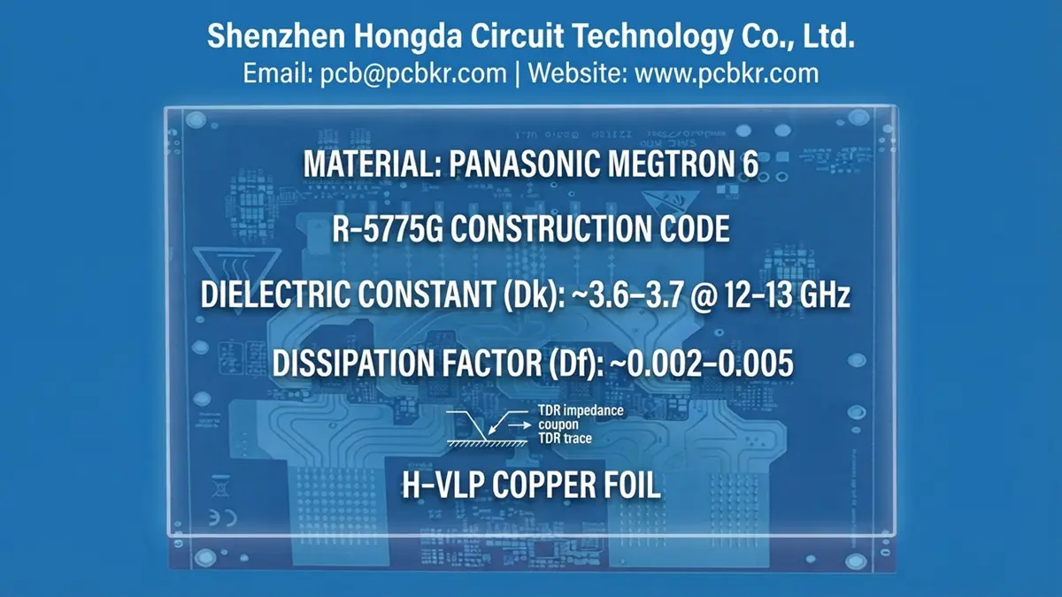
R-5775G PCB Manufacturing: Material Properties, Stackup, Impedance & High-Speed Design
By David Chen, Senior PCB Manufacturing Engineer, Shenzhen Hongda Circuit Technology Co., Ltd. (PCBKR) — 10+ years in high‑speed multilayer PCB fabrication, impedance control, and PCBA. Email: pcb@pcbkr.com
Introduction — What Should You Know Before Buying an R-5775G PCB?
R-5775G PCB Manufacturing is built upon the outstanding performance of Panasonic MEGTRON 6 R-5775G laminate. As a high-performance dielectric material, it is widely specified for high-speed, low-loss multilayer printed circuit boards. Serving as a core substrate for high-frequency and high-speed electronic devices, the R-5775G laminate features ultra-low dielectric constant (Dk) and dielectric loss (Df), which effectively reduces signal attenuation, transmission delay and crosstalk during high-speed signal transmission, meeting the stringent electrical requirements of high-end multilayer PCBs.
However, selecting premium R-5775G laminate is only the starting point of high-quality PCB production and not the decisive factor for final board performance. In actual mass production and custom fabrication of R-5775G PCBs, the final electrical performance, operational stability and long-term reliability of finished boards are determined by the qualified and manufacturing-optimized construction tailored to this laminate material.
The core controllable factors in R-5775G PCB manufacturing cover critical structural design and process control items, including glass style selection, resin content control, precise dielectric thickness management, copper foil profile matching, stackup symmetry optimization, trace geometry design, full fabrication process control, and standardized performance verification methods. All factors are closely correlated and mutually restrictive. Only by strictly standardizing every manufacturing detail based on the inherent characteristics of R-5775G laminate can its high-speed and low-loss advantages be fully realized, ensuring consistent and qualified electrical performance of finished PCBs.
After ten years of fabricating high-speed multilayer boards on Panasonic MEGTRON materials, the single most common mistake I see in RFQs is this: buyers specify only “MEGTRON 6 R-5775G” and assume that guarantees a specific electrical outcome. It doesn’t. Two boards built on the exact same laminate can behave very differently at 10 GHz if the prepreg construction, copper roughness, or lamination control differ.
This guide is written from the manufacturing floor rather than the marketing page. It covers what R-5775G actually is, how its properties vary by test condition, how to engineer a stackup and control impedance around it, where fabrication most commonly goes wrong, and — because this is ultimately a procurement decision — exactly what to put in your RFQ and what to ask a supplier before you place an order.
What Is R-5775G PCB Material?
R-5775G is part of Panasonic’s MEGTRON 6 family of halogen-containing, low-loss laminates and prepregs used in high-speed digital and RF multilayer PCB construction. The MEGTRON 6 series was developed for applications where standard FR-4 cannot hold insertion loss, dielectric stability, or reflow reliability within an acceptable window — high-speed digital backplanes, HDI networking boards, and RF/microwave assemblies.
R-5775G is not a stand-alone product name so much as a construction code within the MEGTRON 6 line: R-5775 is the base laminate, and the (G) suffix designates a specific glass-style and copper-foil pairing on that base resin system.
Where Does R-5775G Fit Within the MEGTRON 6 Family?
Panasonic markets several closely related grades under similar part numbers: R-5775, R-5775G, R-5775K, and R-5775N. They share the same resin chemistry family but differ in glass-cloth construction (standard E-glass vs. low-Dk glass cloth) and copper-foil treatment (H-VLP copper roughness profile). Panasonic’s own technical literature groups R-5775(K) and R-5775(G) together as sharing the same “normal glass cloth” construction, while R-5775(N) uses a low-Dk glass cloth for a lower, more stable dielectric constant.
Why Does the “G” Variant Matter?
In practice, many supplier product pages simply print “R-5775G” without distinguishing it from the closely related K or N grades. That is a real gap in the current market content, and it is also a real procurement risk: substituting one grade for another changes glass style and therefore changes effective Dk, which changes trace geometry needed to hit a target impedance. If your RFQ does not name the exact suffix and glass style, you have not actually specified the material — you have specified a family of materials with different electrical behavior.
What Are the Key R-5775G Material Properties?
Based on Panasonic’s published technical data for the R-5775(K)/R-5775(G) construction (standard E-glass cloth, H-VLP copper):
| Property | Test Method | Typical Value |
|---|---|---|
| Glass transition temperature (Tg) | DSC, IPC-TM-650 | 185°C |
| Time to delamination (T288, with copper) | IPC-TM-650 2.4.24.1 | > 120 min |
| CTE, Z-axis, below Tg (α1) | IPC-TM-650 2.4.24 | 45 ppm/°C |
| CTE, Z-axis, above Tg (α2) | IPC-TM-650 2.4.24 | 260 ppm/°C |
| Dielectric constant (Dk) | IPC-TM-650 2.5.5.9 / balanced-type circular disk resonance | ~3.6–3.7, frequency-dependent |
| Dissipation factor (Df) | Same methods | ~0.002–0.005, frequency-dependent |
This is the single most important engineering point in this entire article: Dk and Df are not fixed constants for “R-5775G.” Panasonic’s own datasheets report different Dk/Df pairs depending on test frequency (1 GHz vs. 10–13 GHz), test method (IPC-TM-650 2.5.5.9 vs. the balanced-type circular disk resonance method used above ~2 GHz), and the specific glass style and resin content of the finished laminate/prepreg combination actually used in your stackup.
That is exactly why different supplier pages quote different Dk numbers for what they call “R-5775G” — some are quoting 1 GHz values, some are quoting values at 10–13 GHz, and some are quoting a nearby grade’s datasheet by mistake. A properly written technical spec always states:
- Test frequency
- Test method
- Glass style (standard E-glass vs. low-Dk glass)
- Resin content and core/prepreg construction
- Whether the number is a datasheet (raw material) Dk or an effective Dk measured on the finished, laminated board
Effective Dk on a finished multilayer board is always the number that should drive your impedance calculation — not the raw laminate datasheet value.
What Is the Difference Between R-5775G, R-5775K and R-5775N?
| Grade | Glass Style | Typical Dk (12–13 GHz) | Notes |
|---|---|---|---|
| R-5775(N) | Low-Dk glass cloth | ~3.3–3.4 | Lower, more stable Dk; often used where tighter impedance/insertion-loss control is required |
| R-5775(K) / R-5775(G) | Standard E-glass cloth | ~3.6–3.7 | Same base resin family, standard glass construction |
Procurement questions this raises:
- Can a manufacturer substitute R-5775G with R-5775N without engineering sign-off? — No. The glass style change alone shifts Dk enough to require trace-width and dielectric-height recalculation to hold the same impedance target.
- Is R-5775G interchangeable with R-5775? — Only if the exact glass cloth and copper foil designation matches; “R-5775” alone is an incomplete part number.
- Can a PCB factory change glass style without approval? — This should be explicitly prohibited in your fabrication drawing and RFQ notes.
- Should the RFQ specify the exact material grade? — Yes, down to the full Panasonic part number, not just “MEGTRON 6.”
- Does changing prepreg change impedance? — Yes; prepreg resin content and dielectric thickness are direct inputs into any impedance calculation.
How Should You Design an R-5775G PCB Stackup?
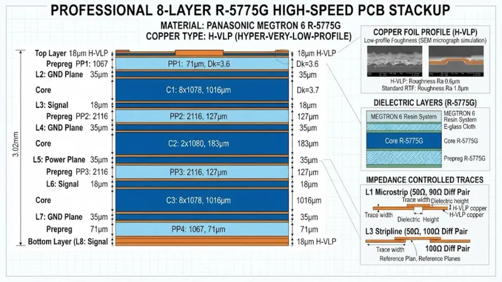
Professional 8-Layer R-5775G High-Speed PCB Stackup
Stackup design is where most of the real engineering work happens — and where most of the value in an R-5775G board is actually created or lost. The examples below are illustrative constructions, not a fixed “R-5775G standard stackup.” Actual finished dielectric thickness, copper weight, and layer count depend entirely on your electrical requirements, layer budget, and target impedance.
Illustrative Stackup A — 4-Layer
- L1 Signal
- L2 Ground (reference plane)
- L3 Power / Signal
- L4 Signal
Illustrative Stackup B — 8-Layer High-Speed
- L1 Signal
- L2 Ground
- L3 Signal
- L4 Ground
- L5 Power
- L6 Signal
- L7 Ground
- L8 Signal
Illustrative Stackup C — 12-Layer High-Speed A 12-layer high-speed construction typically alternates signal layers with continuous ground/power reference planes, uses core and prepreg combinations selected to hit a target finished dielectric height for each impedance-controlled layer, and keeps a symmetric copper distribution top-to-bottom to reduce warpage during lamination.
For every stackup, a competent fabricator should be able to state, layer by layer: core vs. prepreg construction, copper weight, finished dielectric thickness (not nominal), and which layer is the reference plane for each signal layer. If a quote does not include this, the “stackup” you were shown is a drawing, not an engineering deliverable.
How Do You Control 50 Ω and 100 Ω Impedance on R-5775G?
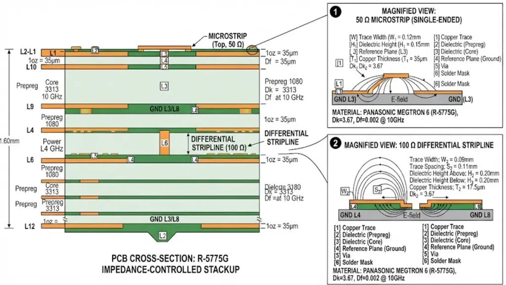
R-5775G Impedance Controlled Microstrip and Stripline Cross-Section
R-5775G boards typically need to hold several impedance targets simultaneously: 50 Ω single-ended, 90 Ω differential, and 100 Ω differential, across microstrip, stripline, and coplanar waveguide with ground (CPWG) topologies depending on the layer and application.
What Determines R-5775G Impedance?
Characteristic impedance on any stripline or microstrip structure is a function of:
- Trace width
- Copper (trace) thickness
- Dielectric height to the nearest reference plane
- Dielectric constant (Dk) of the actual finished construction
- Conductor geometry (microstrip, stripline, or CPWG with ground-via spacing)
Because Dk on R-5775G varies with glass style, resin content, and frequency (as covered above), impedance modeling should always use the effective Dk of your specific finished stackup, verified against Panasonic’s datasheet condition closest to your operating frequency — not a single generic number pulled from a competitor’s product page.
Why Can Two R-5775G PCBs Require Different Trace Widths?
This is one of the most common points of confusion in RFQs, and it’s worth explaining plainly: two boards can both legitimately be called “R-5775G” and still need different trace widths to hit 50 Ω, because they differ in finished dielectric thickness, copper weight, or exact glass/resin construction. A trace width that hits 50 Ω on one fabricator’s stackup will not automatically hit 50 Ω on another’s. This is why an impedance target belongs in your fabrication drawing — the trace width is the fabricator’s output, not your input.
How Does R-5775G Construction Affect High-Speed Signal Integrity?
Signal integrity on an R-5775G board is shaped by more than the base laminate choice. The variables that actually drive insertion loss, return loss, propagation delay, skew, and crosstalk include:
- Dk/Df variation across frequency and construction
- Glass-weave effect (periodic Dk variation along a trace crossing a woven glass style)
- Resin content and dielectric thickness uniformity
- Copper roughness at the conductor-dielectric interface
The key differentiating point: same laminate family does not mean same finished transmission-line performance. Treating “R-5775G” as a single, fixed electrical environment is a common and costly assumption. Two boards on the same base material, but with different copper roughness or dielectric thickness, can show a measurably different insertion-loss curve at 10+ GHz.
How Does Copper Roughness Affect R-5775G High-Speed PCB Loss?
Copper roughness is one of the most under-explained variables in R-5775G procurement, even though it is frequently listed as a spec (H-VLP vs. RTF copper) without explanation of why it matters.
At high frequency, current concentrates near the conductor surface (the skin effect). A rougher copper-dielectric interface forces that surface current to travel a longer effective path, which increases conductor loss — on top of whatever dielectric loss the laminate itself contributes. This is why R-5775G is commonly paired with H-VLP (Hyper-Very-Low-Profile) copper rather than standard RTF (reverse-treated foil) copper in high-speed designs: lower profile copper reduces the added conductor loss at the frequencies where MEGTRON 6 is typically specified.
The practical procurement takeaway: if a supplier quotes “R-5775G” but does not specify the copper foil profile, you do not yet know the actual high-frequency loss performance of the board you are buying.
What Manufacturing Challenges Does R-5775G PCB Fabrication Create?
This is the section that matters most from a buyer’s perspective, because it answers the real question behind most R-5775G RFQs: what actually goes wrong, and what should a qualified fabricator be controlling for?
In my experience, the single biggest pain point in R-5775G (and MEGTRON 6 generally) fabrication is holding a consistent, verified finished dielectric thickness and copper distribution through lamination on a resin system that behaves differently from standard FR-4 under heat and pressure. Everything else — impedance repeatability, insertion-loss consistency, warpage, and via reliability — traces back to how well that one variable is controlled.
Broken down by process step:
① Lamination Dielectric thickness control, resin flow behavior, copper distribution across the panel, multilayer registration accuracy, and warpage control under the specific press cycle this resin system requires.
② Drilling Hole-wall quality, aspect-ratio limits on thicker high-layer-count boards, drill-bit wear rate on this glass style, and smear control before plating.
③ Plating Copper thickness uniformity, plated-through-hole and via reliability, and plating distribution consistency across dense HDI patterns.
④ Imaging Fine-line registration and layer-to-layer alignment accuracy, particularly on impedance-controlled traces where a few microns of width variation shifts the measured impedance.
⑤ Surface Finish ENIG, ENEPIG, or OSP, selected based on the assembly process, contact requirements, and shelf-life needs of the specific application.
How Should a Manufacturer Control R-5775G Lamination and Registration?
Any supplier can claim “we can do MEGTRON 6.” The real procurement question is: can they prove it’s stable, board after board?
Rather than listing equipment names, a credible answer to this question should walk through a control chain:
Lamination recipe → press cycle control → resin flow and copper balance → registration accuracy → finished dielectric thickness measurement → impedance coupon correlation → cross-section and microsection verification.
At PCBKR, this is how we approach it in practice. Our vacuum lamination presses are set up with resin-flow and press-cycle profiles specific to MEGTRON 6 material behavior — not a generic FR-4 cycle — because R-5775G’s cure characteristics and CTE profile above Tg (α2 ≈ 260 ppm/°C per Panasonic’s published data) demand tighter thermal and pressure control to avoid resin voiding and copper distribution shifts. Laser Direct Imaging (LDI) is used on impedance-controlled layers because it holds tighter line-width tolerance than conventional phototool imaging, which matters directly for trace-width-driven impedance accuracy. Controlled-depth laser and mechanical drilling combinations are selected by hole aspect ratio to manage smear and wall quality on higher layer-count constructions.
The point of naming this equipment is not the equipment itself — it’s the fact that each piece of equipment maps to a measurable output that a buyer can actually request in an inspection report: finished dielectric thickness readings, registration offset data, and impedance coupon TDR traces. That measurable-output chain is what should influence your evaluation of a supplier’s manufacturing keyword claims (“advanced equipment,” “high-speed PCB capability”) far more than the equipment list on its own.
How Is R-5775G PCB Impedance Verified?
Impedance should never be accepted on the strength of a calculation alone. A proper verification process includes:
- A dedicated impedance coupon built on the same panel, same layer, same construction as the production traces
- TDR (Time Domain Reflectometry) measurement of single-ended and differential impedance
- A stated test frequency and test location on the coupon
- Documented trace geometry used for the measurement
- A stated tolerance (commonly ±10% for standard controlled-impedance work, tighter for high-speed differential pairs)
- A test report delivered with the shipment, not just available on request
Buyers should request this test report as a standard deliverable in the RFQ, not as an afterthought at inspection.
What Reliability Tests Should You Request for an R-5775G PCB?
For high-speed and RF applications built on R-5775G, a reasonable reliability package includes microsection analysis, thermal stress testing (reflow cycling), solder resistance testing, via reliability assessment, Interconnect Stress Testing (IST) where applicable, electrical continuity/isolation testing, impedance testing, dimensional inspection, and material certification traceable to Panasonic.
The real procurement pain point here: what evidence should a supplier provide instead of simply claiming “high reliability”? The answer is the documentation above — a claim without a test report or microsection image is not verifiable and should not be accepted as sufficient for a high-speed or RF program.
Which Applications Use R-5775G High-Speed PCBs?
- AI / Data Center: AI servers, accelerator systems, high-speed networking switches, backplanes
- Telecom: routers, switches, optical networking equipment, base stations
- RF: RF front-end modules, microwave assemblies, mmWave-adjacent designs
- Industrial / Test: measurement equipment, high-speed instrumentation
MEGTRON 6-family laminates are widely referenced in RF component manufacturer application notes as a suitable substrate class for 50 Ω controlled-impedance CPWG designs at microwave and mmWave frequencies, which reflects the material’s role beyond digital backplanes into RF and test-and-measurement hardware.
Can R-5775G Be Used for RF and Microwave PCB Designs?
Yes. R-5775G’s low-loss, stable dielectric properties make it suitable for 50 Ω CPWG, microstrip RF transitions, and connector launch designs. For RF applications, the design details that matter most are dielectric thickness under the RF trace, RF trace geometry (width and gap to ground), ground-via placement and spacing around the transition, and pad-to-trace transition geometry at the RF connector or component launch. These should always be engineered against your specific component’s PCB layout recommendations and verified on your actual finished stackup — not copied from a generic reference design on a different substrate.
How Should You Specify R-5775G in a PCB RFQ?
This is the most commercially important section of this guide. Use the checklist below as a minimum RFQ specification.
Material
- Manufacturer (Panasonic)
- Exact grade and suffix (R-5775G, not just “MEGTRON 6”)
- Full construction: core and prepreg part numbers
- Glass style
Board
- Layer count
- Finished board thickness
- Board dimensions
- Copper thickness per layer
- Surface finish
Electrical
- 50 Ω single-ended target
- 90/100 Ω differential targets
- Impedance tolerance
- Insertion-loss target
- Operating frequency / data rate
Manufacturing
- Minimum trace/space
- Via structure (through-hole, blind, buried)
- Aspect ratio limits
- Backdrilling requirements
- Via filling requirements
- Registration tolerance
Quality
- IPC class (e.g., IPC-6012 Class 2 or Class 3)
- Impedance test report
- Microsection report
- Electrical test report
- Material Certificate of Conformance (COC)
- Final inspection report
What Should You Ask an R-5775G PCB Manufacturer Before Placing an Order?
10-Point Supplier Qualification Checklist
- Can you source genuine Panasonic R-5775G, with material certification?
- Can you provide a Certificate of Conformance for the actual material lot used?
- Can you maintain the same approved construction across repeat orders?
- Can you provide a fully documented, layer-by-layer controlled stackup?
- How do you calculate impedance, and against which Dk value?
- Do you provide impedance coupons with every production run?
- What TDR capability do you use for impedance verification?
- Can you provide microsection reports on request?
- How do you control multilayer registration on high-layer-count boards?
- Can you support the same construction from prototype through volume production?
How Much Does R-5775G PCB Manufacturing Cost?
There is no honest single price-per-board figure for R-5775G manufacturing — anyone quoting one without your full specification is guessing. Cost is driven by:
- Layer count and board size
- Order quantity
- Copper weight
- Finished board thickness
- HDI structure (blind/buried vias, microvias)
- Via structure, backdrilling, and via filling
- Surface finish
- Impedance requirements and fabrication tolerance
- Testing scope (impedance coupons, microsection, electrical test)
- Material availability and lead time
Why a low-cost FR-4 quote cannot be directly compared to an R-5775G quote: the material itself carries a premium over standard FR-4, but the larger cost driver is usually the additional process control — tighter lamination cycles, impedance coupon fabrication and testing, and registration control — required to make the material’s performance actually usable at high speed. A quote that matches a generic FR-4 board’s price for an R-5775G build is a signal that some of this process control is likely missing.
What Is the Typical R-5775G PCB Prototype Lead Time?
Rather than a flat “7–10 days” figure, prototype lead time on R-5775G realistically breaks down into:
- Material availability (Panasonic MEGTRON 6 lead time can vary by grade and region)
- Engineering review of the stackup and impedance targets
- Stackup confirmation with the customer
- Lamination
- Fabrication (drilling, plating, imaging, surface finish)
- Testing (impedance, electrical, microsection where required)
- Final inspection
Prototype, small-batch, and volume production timelines differ meaningfully — volume runs benefit from a pre-qualified, locked stackup and material inventory, while first-article prototypes carry additional engineering review and coupon-verification time.
How Do You Choose an R-5775G PCB Manufacturer?
Rather than any claim of being “the best manufacturer,” a verifiable evaluation framework should look at:
- Documented experience with the specific MEGTRON 6 grade you need, not MEGTRON 6 in general
- Willingness to provide layer-by-layer stackup documentation before order placement
- Standard inclusion of impedance coupons and TDR test reports
- Traceable material certification back to Panasonic
- Demonstrated process control at each fabrication step relevant to this resin system
- Ability to hold the same construction from prototype through volume production
What Are the Most Common R-5775G PCB Design and Manufacturing Problems?
- Using one generic Dk value for every stackup, instead of the effective Dk of the actual finished construction.
- Changing prepreg construction without recalculating impedance, which silently shifts trace-width requirements.
- Ignoring copper roughness at high frequency, underestimating conductor loss contribution.
- Using nominal dielectric thickness instead of finished thickness in impedance calculations.
- Treating 50 Ω impedance as a trace-width-only problem, ignoring dielectric height and copper thickness interaction.
- Failing to control glass/resin construction consistency across production lots.
- Not matching the PCB stackup to the RF component’s reference design geometry.
- Approving material substitution without engineering review (e.g., swapping R-5775G for R-5775N).
- No impedance coupon correlation between calculated and measured impedance.
- Supplier provides a material name but not construction-level documentation — no core/prepreg part numbers, no copper foil designation.
What Are the Most Frequently Asked Questions About R-5775G PCB?
What is R‑5775G PCB material?
R‑5775G is a Panasonic MEGTRON 6‑family laminate/prepreg system built on standard E‑glass cloth, used for low‑loss, high‑speed multilayer and RF PCB construction, typically paired with H‑VLP copper foil.
What is the Dk of R‑5775G?
Per Panasonic’s published data for the R‑5775(K)/R‑5775(G) construction, Dk is approximately 3.6–3.7 depending on test frequency and method — around 3.7 at 1 GHz and closer to 3.6 at 12–13 GHz using the balanced‑type circular disk resonance method. This is a datasheet raw‑material value; effective Dk on your finished board should be verified against your specific construction.
Is R‑5775G suitable for high‑speed and RF PCB designs?
Yes. Its low dissipation factor, high Tg (185°C), and long T288 delamination time (>120 minutes with copper) make it suitable for high‑speed digital backplanes, controlled‑impedance boards, and 50 Ω RF designs, provided the stackup, copper foil, and fabrication process are engineered around the specific electrical target.
What is the difference between R‑5775G and R‑5775N?
R‑5775N uses a low‑Dk glass cloth, giving it a lower and more stable Dk (roughly 3.3–3.4 at high frequency) than R‑5775G’s standard E‑glass construction (roughly 3.6–3.7). They are not interchangeable without recalculating impedance and insertion‑loss targets.
What information should be included when requesting an R‑5775G PCB quote?
At minimum: exact material grade and construction (core/prepreg part numbers), layer count and copper thickness, impedance targets and tolerance, minimum trace/space, via structure, surface finish, required IPC class, and the test/inspection reports you require (impedance coupon, microsection, material COC).
About the Author
David Chen https://www.linkedin.com/in/pcbcoming Email: pcb@pcbkr.com
David Chen is a Senior RF/PCB Process Engineer at Shenzhen Hongda Circuit Technology Co., Ltd., with over 12 years of experience in high-frequency PCB fabrication, impedance-controlled stack-up design, and Rogers/PTFE laminate processing. He also boasts an extensive professional background in PCBA manufacturing, PCBA testing, and PCBA optimization, with specialized expertise in high-precision PCBA fault analysis and rigorous PCBA reliability testing. The author has worked with high-layer-count server PCB fabrication, ultra-low-loss backplane stackups, and thermo-mechanical reliability optimization for AI infrastructure projects involving 112G and 224G PAM4 architectures. Skilled in complex circuit design and cutting-edge advanced PCB manufacturing processes, he delivers solutions that elevate product durability and performance across industrial applications. His technical articles focusing on PCBA manufacturing workflows and testing methodologies are widely cited by industry peers and technical platforms, and have gained attention and recognition from industry colleagues.
Standards and sources referenced: Panasonic Industry MEGTRON 6 technical datasheets (R‑5775 series); IPC‑TM‑650 test methods (2.4.24, 2.4.24.1, 2.5.5.9); IPC‑6012 acceptance requirements for rigid printed boards; IPC‑2141 controlled impedance design guidance.
PCBKR (Shenzhen Hongda Circuit Technology Co., Ltd.) manufactures prototype and volume high‑speed multilayer PCBs on Panasonic MEGTRON 6 materials including R‑5775G, with in‑house impedance coupon testing, TDR verification, and material traceability. www.pcbkr.com