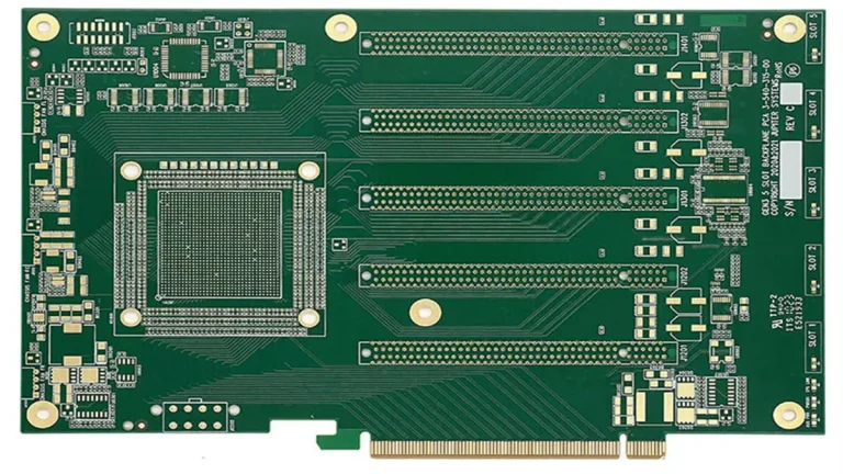
0.5 mm BGA HDI PCB Manufacturer for Fine-Pitch Applications
By a Senior PCB Manufacturing Engineer, 10+ Years in HDI Fabrication — Shenzhen Hongda Circuit Technology Co., Ltd. (www.pcbkr.com)
Routing a 0.5 mm pitch BGA is one of the most common — and most misunderstood — challenges in modern PCB fabrication. Over more than a decade of production engineering, I have reviewed thousands of 0.5 mm BGA HDI designs, and the failures I see repeatedly are not exotic; they are fundamental mismatches between escape-routing geometry, microvia structure, and the fabricator’s actual process capability. This guide is written from the fabrication floor, not from a datasheet, and it reflects the standards, equipment, and process windows we run daily at Shenzhen Hongda Circuit Technology (Hongda PCB).
A 0.5 mm pitch BGA almost always requires HDI (High Density Interconnect) construction — typically 1+N+1 or 2+N+2 stackups with laser-drilled microvias — because the 0.5 mm pad pitch leaves too little room for a conventional through-hole escape trace between adjacent pads. The correct structure depends on ball count, layer count, signal integrity requirements, and cost targets, which we break down in detail below.
What 0.5 mm BGA HDI PCB Manufacturing Capability Do You Need?
Before selecting a fabrication partner, you need to confirm four capability areas: achievable HDI structures, microvia/via technology, line-and-space limits, and inspection depth. A supplier that cannot demonstrate all four with data — not just a capability chart — is a production risk for 0.5 mm pitch work.
What HDI structures can be manufactured?
At Hongda PCB, our standard 0.5 mm BGA HDI capability spans 1+N+1, 2+N+2, and any-layer (stacked/staggered microvia) constructions, built per IPC-2226 class definitions for HDI structures. Most 0.5 mm pitch designs with moderate ball counts (under ~400 I/O) resolve cleanly with 1+N+1; higher-density devices and packages with multiple inner rows typically require 2+N+2 or stacked microvias to fully escape the array.
What microvia and via technologies are available?
Our microvia process uses CO2 and UV laser drilling depending on dielectric type and target via diameter, with typical finished microvia diameters from 75 µm to 100 µm and aspect ratios controlled to IPC-2226 recommendations. We support laser-drilled blind vias, mechanically-drilled buried vias, stacked microvias, staggered microvias, and via-in-pad with copper fill and cap plating.
What line/space and layer-count capabilities apply?
Fine-pitch BGA escape routing on our lines typically achieves 2.5/2.5 mil (60/60 µm) trace/space in production, with tighter geometries achievable for qualified designs. Layer counts for 0.5 mm BGA HDI boards commonly range from 8 to 24+ layers, depending on signal count, power distribution, and impedance-controlled layer requirements.
What inspection and testing are available?
Every 0.5 mm BGA HDI panel passes through automated optical inspection (AOI) after imaging and etching, X-ray inspection for buried/blind via and via-in-pad integrity, microsection (cross-section) analysis for first-article and periodic process validation, and 100% electrical test (flying probe or fixture, depending on volume) prior to shipment, consistent with IPC-6012 acceptance criteria for rigid PCBs.
Why Does a 0.5 mm BGA Usually Need HDI Routing?
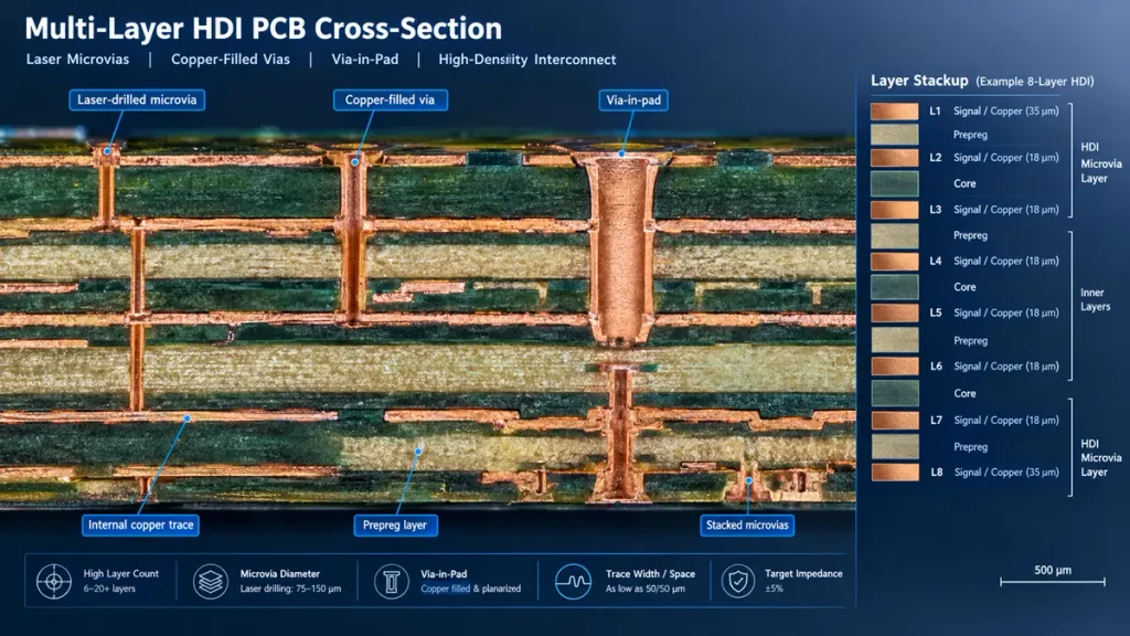
Multi-Layer HDI PCB Cross-Section and Layer Stackup Analysis
How does BGA pitch affect escape routing?
At 0.5 mm pitch, the center-to-center pad spacing is only 500 µm, and typical pad diameters run 250–280 µm, leaving roughly 220–250 µm of channel between adjacent pads. That channel has to carry the escape trace, the annular clearance, and any solder mask registration tolerance — which is why pitch, not layer count alone, is the real driver of HDI necessity.
Why does conventional dog-bone routing become difficult?
Conventional dog-bone routing pulls each BGA pad out to a via placed beside the pad, then routes from the via. At 0.5 mm pitch, there is not enough room to place a mechanically-drilled through-via (typically 200 µm+ finished hole) beside the pad without violating annular ring or spacing rules on the outer rows, and inner-row balls have no clear escape path at all once you run out of channels.
When can conventional routing still work?
Conventional (non-HDI) routing can still work for 0.5 mm BGAs with low ball counts and a simple perimeter-only array — for example, small footprint devices with two or three signal rows and generous ground/power ball placement. Once the array grows past roughly 8×8 with multiple internal signal rows, HDI escape becomes effectively mandatory.
How Should You Choose the HDI Structure for a 0.5 mm BGA?
When is 1+N+1 sufficient?
1+N+1 (one laser-drilled microvia layer on each side of a conventional core) is typically sufficient for 0.5 mm BGAs up to roughly 300–400 balls with a moderate number of internal signal rows, where via-in-pad on the outer 1–2 rows and standard dog-bone on the remaining rows can fully escape the array.
When is 2+N+2 required?
2+N+2 becomes necessary when the device has three or more internal signal rows that cannot reach a routing layer through a single microvia hop, or when the design needs additional HDI layers to separate high-speed differential pairs from noisy digital or power routing without cross-talk.
When are stacked microvias justified?
Stacked microvias — laser vias drilled directly on top of one another through sequential lamination cycles — are justified when board thickness and layer count must be minimized despite very high ball density, such as in mobile, wearable, or module products where z-height is constrained. Stacking adds cost and requires tighter process control, so it should be specified only when staggered microvias cannot meet the escape requirement.
Can partial HDI reduce complexity and cost?
Yes. A partial (selective) HDI layer — laser microvias only in the BGA escape region, with the rest of the board using standard mechanical vias — is a common cost-reduction strategy for boards where only one or two high-density components drive the HDI requirement.
How Should You Design the 0.5 mm BGA Escape Routing?
How do pad size and pitch affect routing?
Pad diameter should generally be kept to 60–65% of pitch for 0.5 mm BGAs (roughly 250–280 µm) to preserve trace channel width; oversized pads are one of the most common design errors we see, and they eliminate routing options before fabrication even begins.
Can traces pass between BGA pads?
Yes, but only with tightly controlled geometry. Passing one trace between adjacent 0.5 mm pads generally requires trace width and clearance at or below 3 mil (75 µm) on each side, which must match the fabricator’s proven production capability — not just their minimum-feature datasheet number.
How should inner BGA rows escape?
Inner rows escape through microvias placed directly in the pad (via-in-pad) or immediately adjacent to it, dropping the signal to an inner routing layer before it needs to cross other pads. This is the primary reason 0.5 mm BGA arrays with more than two internal rows require HDI rather than surface escape.
How do ball count and array size affect layer count?
As a practical rule from production experience: every additional fully-populated internal row typically adds one dedicated HDI escape/routing layer pair. A 15×15 fully populated array will typically need two to three more routing layers than a comparable 10×10 array at the same pitch.
What Via-in-Pad Design Rules Matter for 0.5 mm BGA?
Via-in-pad vs dog-bone
Via-in-pad places the microvia directly inside the component pad, eliminating the need for a separate escape trace segment and saving critical channel space — essential at 0.5 mm pitch. Dog-bone routing, which pulls the via out beside the pad, is only viable where channel width allows both a via and a trace.
Microvia diameter
Standard via-in-pad microvia diameters for 0.5 mm BGA work run 75–100 µm finished, sized to fit inside the pad with adequate annular clearance per IPC-2226 while keeping the capture pad within the 250–280 µm pad footprint.
H3: Via filling
Via-in-pad structures must be resin- or copper-filled (per IPC-4761 Type VII) to prevent solder wicking into the via during reflow and to provide a flat, solderable surface. Unfilled via-in-pad is not acceptable for 0.5 mm BGA assembly.
Planarization
After filling, the via cap must be planarized (typically via cap plating and mechanical/chemical planarization) to hold flatness within a few microns across the pad — poor planarization is a leading cause of head-in-pillow and open-solder-joint defects at fine pitch.
VIPPO
VIPPO (Via-In-Pad Plated Over) is the standard construction for 0.5 mm BGA via-in-pad: the filled via is capped with plated copper, producing a continuous, solderable pad surface. This is the construction we specify by default for fine-pitch via-in-pad work.
H3: Solder mask and pad definition
Solder mask registration tolerance becomes critical at 0.5 mm pitch; we recommend non-solder-mask-defined (NSMD) pads wherever the channel width allows, reserving solder-mask-defined (SMD) pads for the tightest via-in-pad cases where mask registration risk must be minimized.
How Should You Select the Stackup and Materials?
Stackup and BGA escape
The stackup must be designed around the BGA escape requirement first, then extended for power/ground planes and signal routing. We typically place the first HDI microvia layer pair immediately adjacent to the component side to minimize via stub length and preserve signal integrity for high-speed pins.
FR-4 vs high-Tg
Standard FR-4 (per IPC-4101) is adequate for many 0.5 mm BGA HDI boards, but high-Tg FR-4 (Tg ≥ 170°C) is recommended whenever the board will see multiple lead-free reflow cycles or rework, since sequential lamination for HDI structures adds thermal cycles beyond a standard board build.
Low-loss materials
For BGAs carrying high-speed serial links (PCIe, DDR4/5, SerDes above a few Gbps), low-loss or mid-loss laminates are recommended to control insertion loss and maintain signal integrity across the microvia transitions, which introduce additional impedance discontinuities compared to a single-layer board.
Copper thickness
Inner-layer copper for HDI escape layers is typically specified at 0.5 oz (17 µm) or lighter to hold fine line/space tolerance, while outer layers and power planes may use 1 oz or heavier copper depending on current-carrying requirements.
Impedance control
Controlled impedance is mandatory for any high-speed signal escaping a 0.5 mm BGA. We validate stackup impedance with 2D field-solver modeling before fabrication and confirm on production panels with TDR (time-domain reflectometry) testing per IPC-TM-650 Method 2.5.5.7.
What DFM Problems Can Cause a 0.5 mm BGA HDI PCB to Fail?
In our production experience, this is where the biggest pain point in 0.5 mm BGA HDI manufacturing actually lives: not any single process step, but the cumulative registration budget across sequential lamination cycles. Each additional HDI layer pair adds its own layer-to-layer registration tolerance, and at 0.5 mm pitch that budget is consumed almost entirely before the board reaches final drilling.
Registration
Layer-to-layer registration error is the single most common root cause of 0.5 mm BGA HDI yield loss. Even a 25–30 µm shift between the core and a laser-drilled layer can cause a microvia to miss its target pad, and this risk compounds with every additional sequential lamination cycle in a 2+N+2 or stacked-microvia build.
Microvia defects
Incomplete laser ablation, resin smear left in the via after desmear, and voiding in copper-filled vias are the most frequent microvia defects. These are controlled through laser parameter calibration by material lot, plasma or wet desmear process control, and via-fill process validation with cross-section sampling.
Via-in-pad defects
Voiding inside filled via-in-pad structures is a critical defect because it is invisible on the surface but causes solder-joint failure during assembly or thermal cycling in the field. We control this with X-ray inspection of 100% of via-in-pad structures on high-reliability orders and periodic destructive microsection sampling.
Solder mask limitations
At 0.5 mm pitch, solder mask dam width between adjacent pads can fall below the reliable minimum for standard liquid photoimageable (LPI) mask, leading to mask webbing, bridging, or dam lifting. This is one reason pad size and mask dam width must be reviewed together during DFM, not treated as independent design rules.
Trace/space
Trace and space below roughly 3 mil (75 µm) pushes conventional subtractive etching close to its resolution limit; we hold this class of feature to LDI (laser direct imaging) exposure with tightened etch-compensation to avoid open or shorted traces in the BGA escape field.
Impedance variation
Dielectric thickness variation introduced by sequential lamination — particularly around laser-drilled microvia fields where resin flow behaves differently than in solid copper areas — can shift impedance by several ohms if not compensated in the stackup design and confirmed with production TDR data.
How Is a 0.5 mm BGA HDI PCB Manufactured and Inspected?
This is where advanced fabrication equipment directly determines whether a 0.5 mm BGA design is manufacturable at all. Our production line for fine-pitch HDI work includes UV/CO2 laser drilling systems, LDI exposure, sequential vacuum lamination presses, automated electroless and pattern plating lines, and full AOI/X-ray/electrical test coverage — the combination that keeps registration and microvia defect rates low enough for high-density escape routing.
CAM and DFM
Every 0.5 mm BGA HDI order goes through engineering DFM review before CAM release, checking pad geometry, via-in-pad fill/cap specification, drill-to-copper clearance, and layer registration budget against our qualified process window.
Sequential lamination
Each HDI layer pair is built through a separate lamination, laser-drill, and plate cycle; a 2+N+2 build requires at least two full sequential lamination passes beyond the core, which is why registration control at each pass is the dominant process risk.
Laser drilling
CO2 lasers are typically used for larger-diameter microvias in standard FR-4, while UV lasers provide the finer diameter and cleaner wall quality needed for the smallest via-in-pad structures and low-loss laminates.
Microvia plating
After desmear, microvias are metallized through electroless copper deposition followed by electrolytic pattern or panel plating, with plating thickness and via-wall coverage confirmed by cross-section per IPC-6012 Class 3 requirements for high-reliability boards.
Via filling
Copper or conductive/non-conductive resin fill is applied per via-fill specification, followed by cap plating for VIPPO structures, with process control targeting <5% void rate confirmed by X-ray and cross-section sampling.
Surface finishing
ENIG (electroless nickel immersion gold) is our default surface finish recommendation for 0.5 mm BGA via-in-pad assemblies because of its flatness and solderability; ENEPIG is used where wire-bond compatibility or additional gold-wire-bond reliability is required.
AOI
Automated optical inspection runs after inner-layer imaging/etching and again after outer-layer processing, catching open, short, and trace-width defects before the panel advances to drilling and lamination of the next HDI layer.
X-ray
X-ray inspection verifies microvia and via-in-pad fill integrity, buried via alignment, and layer-to-layer registration on structures that cannot be visually confirmed after lamination.
Electrical testing
100% electrical test — flying probe for prototype/low volume, dedicated fixture for production volume — confirms continuity and isolation across every net before shipment.
Microsection
Destructive microsection (cross-section) analysis on coupon samples from each production lot confirms via wall plating thickness, via-fill void rate, and layer registration, providing objective process data rather than visual estimation.
How Do You Verify Reliability Before Volume Production?
Microsection
First-article microsection is standard practice before releasing a new 0.5 mm BGA HDI design to volume, confirming that microvia structure, plating thickness, and registration all meet specification on the actual tooling before hundreds or thousands of panels are committed.
X-ray
Production-lot X-ray sampling continues through volume manufacturing to catch process drift in via-fill quality or registration that a first-article sample alone would not reveal.
Impedance testing
TDR-based impedance verification on production coupons, per IPC-TM-650 Method 2.5.5.7, confirms that the fabricated stackup matches the simulated impedance target within the specified tolerance (typically ±10%).
Reliability testing
For high-reliability applications, thermal cycling and interconnect stress testing per IPC-9701 (or customer-specific reliability requirements) validates that microvia and via-in-pad structures survive the expected field thermal environment.
Quality documentation
A complete quality package — cross-section reports, X-ray records, electrical test data, and material certifications traceable to IPC-6012 Class 2 or Class 3 acceptance — should be available for every production lot, not just on request for audits.
What Manufacturing Factors Affect 0.5 mm BGA HDI PCB Cost?
HDI order
Moving from 1+N+1 to 2+N+2 or stacked microvia adds a full sequential lamination cycle, which is typically the single largest cost driver in a 0.5 mm BGA HDI quote.
Layer count
Each additional layer pair adds material, imaging, drilling, and plating cost; layer count driven purely by BGA escape (rather than functional routing need) is the first place to look for cost reduction during DFM.
Microvia
Smaller microvia diameters and tighter aspect ratios require more laser passes and tighter process control, increasing cost per hole compared to standard-diameter microvias.
Via filling
Copper-filled via-in-pad is more expensive than resin-filled or unfilled microvias due to additional plating time and cap-planarization steps, but it is generally non-negotiable for reliable 0.5 mm BGA assembly.
Material
Low-loss and high-Tg laminates cost more than standard FR-4 and should be specified only where the electrical or thermal requirement genuinely demands it.
Copper
Heavier copper weights on HDI layers work against fine line/space capability and add etching cost; copper weight should be matched to actual current requirements per layer rather than applied uniformly.
Surface finish
ENIG and ENEPIG cost more than HASL or OSP but are effectively required for 0.5 mm BGA via-in-pad flatness and solderability, making this a necessary cost rather than a discretionary one.
Testing
100% electrical test, X-ray sampling, and microsection analysis all add direct cost but are the controls that prevent field failures in fine-pitch assemblies — reducing testing scope on 0.5 mm BGA work is a false economy.
Quantity
As with most PCB fabrication, panel utilization and volume significantly affect unit cost; prototype and low-volume 0.5 mm BGA HDI boards carry a substantial premium over production-volume panels due to tooling and setup amortization.
How Does 0.5 mm BGA HDI PCB Lead Time Depend on the Design?
Lead time scales primarily with the number of sequential lamination cycles, not overall layer count alone. A 1+N+1 build with straightforward via-in-pad typically runs on our standard HDI lead time; a 2+N+2 or stacked-microvia build adds a full additional lamination-drill-plate cycle, commonly extending lead time by several working days. Tight registration tolerances, copper-filled via-in-pad, and impedance-controlled stackups with TDR verification each add incremental engineering and process time on top of the base HDI cycle.
Which Applications Use 0.5 mm BGA HDI PCBs?
0.5 mm pitch BGA HDI construction is standard in smartphone and wearable mainboards, network switching and routing modules, high-density FPGA and SoC carrier boards, automotive ADAS and infotainment modules, medical imaging and diagnostic devices, and compact power-management or RF modules — essentially any product where package density has outpaced what conventional through-hole routing can escape.
What Should You Send a Manufacturer for a 0.5 mm BGA HDI PCB Quote?
For an accurate, actionable quote, provide: Gerber (RS-274X) or ODB++/IPC-2581 fabrication data, IPC netlist for DRC cross-check, stackup drawing with target impedance and dielectric requirements, drill file with via-in-pad and fill callouts clearly noted, surface finish and solder mask/legend specification, and any customer-specific reliability or acceptance class requirement (e.g., IPC-6012 Class 2 or Class 3). Including the actual BGA datasheet or footprint drawing lets the fabricator confirm pad size, pitch, and escape feasibility before quoting rather than after tooling.
How Should You Evaluate a 0.5 mm BGA HDI PCB Manufacturer?
Evaluate a fine-pitch HDI supplier on demonstrated process capability (not catalog minimums), equipment for laser drilling, sequential lamination, and via-fill/planarization, inspection depth (AOI, X-ray, microsection, electrical test coverage), quality system and traceability documentation, and willingness to review DFM before quoting rather than after fabrication has started. A supplier that asks clarifying DFM questions about your via-in-pad and registration requirements before quoting is, in our experience, a stronger predictor of yield than any single capability spec sheet.
Frequently Asked Questions About 0.5 mm BGA HDI PCBs
Does every 0.5 mm pitch BGA require HDI construction?
Not always. Low ball-count devices with a simple perimeter array can sometimes be routed conventionally. Once internal rows and higher ball counts are involved, HDI is generally required.
What is the minimum microvia diameter for 0.5 mm BGA via-in-pad?
Typical finished microvia diameters run 75–100 µm, sized to fit within a 250–280 µm pad with adequate annular clearance.
Is via-in-pad required for 0.5 mm BGA, or is dog-bone routing acceptable?
Via-in-pad is required wherever channel width does not allow a separate escape via beside the pad — which, at 0.5 mm pitch, is most of the array except possibly the outermost row.
What surface finish is recommended for 0.5 mm BGA HDI boards?
ENIG is the standard recommendation for flatness and solderability; ENEPIG is used when wire-bond compatibility is also required.
How many layers does a typical 0.5 mm BGA HDI board need?
This depends on ball count and internal row count, but production designs commonly range from 8 to 24+ layers.
What is the difference between 1+N+1 and 2+N+2 HDI structures?
1+N+1 has one laser-drilled microvia layer on each side of the core; 2+N+2 has two, allowing deeper escape for higher ball counts or additional internal signal rows.
Can partial (selective) HDI reduce cost on a 0.5 mm BGA design?
Yes, when only one or two components on the board actually require HDI escape, applying laser microvias only in that region — rather than across the whole board — can meaningfully reduce cost.
How Can You Request a Quote for a 0.5 mm BGA HDI PCB?
Shenzhen Hongda Circuit Technology Co., Ltd. manufactures 0.5 mm BGA HDI PCBs from prototype through volume production, with in-house laser drilling, sequential lamination, via-fill/planarization, and full AOI/X-ray/electrical inspection. To get an accurate quote and DFM review, send your Gerber/ODB++ data, stackup and impedance requirements, and BGA footprint details through www.pcbkr.com, and our engineering team will confirm escape-routing feasibility and process fit before tooling begins.
About Author
David Chen https://www.linkedin.com/in/pcbcoming
David Chen boasts an extensive professional background in PCBA manufacturing, PCBA testing, and PCBA optimization, with specialized expertise in high-precision PCBA fault analysis and rigorous PCBA reliability testing. The author has worked with high-layer-count server PCB fabrication, ultra-low-loss backplane stackups, and thermo-mechanical reliability optimization for AI infrastructure projects involving 112G and 224G PAM4 architectures. Skilled in complex circuit design and cutting-edge advanced PCB manufacturing processes, he delivers solutions that elevate product durability and performance across industrial applications. His technical articles focusing on PCBA manufacturing workflows and testing methodologies are widely cited by industry peers, research institutions, and technical platforms, solidifying his reputation as a recognized technical authority in the global circuit board manufacturing sector.