Who Manufactures PCBs for AI Server OEMs?
Shenzhen Hongda Circuit Technology Co., Ltd. manufactures PCBs for AI server OEMs — building 20- to 60-layer HDI boards on Megtron 6/7/8 and Tachyon 100G laminates, holding ±5% impedance tolerance, and validating every panel with TDR and 100% netlist testing before it ships to a GPU baseboard or NVLink switch program.
That one-line answer covers the “what.” The rest of this page covers the “how” and the “why it’s hard” — the layer stacks, the material chemistry, the backdrilling tolerances, and the yield math that separate a board that survives a 700W GPU rack from one that comes back as a field return six months later.
What Makes an AI Server PCB Different From a Standard Server Board?
An AI server PCB carries 20–60+ copper layers instead of the 8–16 layers typical of a standard 1U/2U server board, routes SerDes lanes at 112G or 224G PAM4 instead of 10–25G NRZ, and depends on laminates with Df below 0.004 instead of FR-4’s 0.015–0.02 — because GPU-to-GPU and GPU-to-switch links at these speeds have almost no loss budget left to spend on the board itself.
A standard server motherboard moves data at PCIe Gen3/Gen4 speeds (8–16 GT/s) across maybe 12–16 layers of ordinary FR-4 or low-loss laminate, and a 10% impedance miss is survivable because the link has margin. An AI server board carrying NVLink or PCIe Gen5/Gen6 traffic at 112G PAM4 does not have that margin. At 28 GHz (the effective frequency of a 112G PAM4 lane), standard FR-4 with Df ≈ 0.02 can eat more than 1 dB/inch of signal — on a 20-inch backplane trace that’s a 20 dB loss before the receiver even sees the eye diagram. That’s why our engineering team treats material selection as a signal-integrity decision, not a procurement decision.
In practice we see three things separate AI server projects from everything else that crosses our line: layer count that routinely passes 30L and approaches 60L for OAM/SXM-style baseboards, hybrid stackups that mix Megtron 6/7/8 or Tachyon 100G on the high-speed core with 370HR or standard FR-4 on power/ground layers to control material cost, and tolerance budgets — ±5% controlled impedance, <5% dielectric thickness deviation, <10% copper foil deviation — that would be considered “tight” on a consumer board and are simply “the spec” here.
How Many Layers Does an AI Server PCB Actually Need?
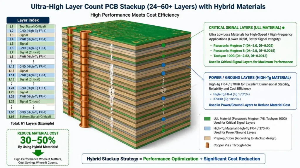
3D Microsection & Layer Index of a 60+ Layer Hybrid AI Server PCB Stackup
GPU baseboards and OAM/HGX modules typically require 24–40 layers, NVLink switch line cards and InfiniBand NDR boards run 28–36 layers, and the largest scale-up backplanes for Blackwell/Rubin-class platforms can exceed 40–60 layers — the exact count is driven by how many independent SerDes lane groups, power planes, and ground reference planes must coexist without crosstalk.
Layer count is not a marketing number; it’s an outcome of three competing layer budgets stacking on top of each other. A modern AI accelerator module needs dedicated layers for: PCIe Gen5/Gen6 and NVLink high-speed differential pairs (each pair ideally sandwiched between solid ground references to control return-path discontinuity), the power delivery network feeding a GPU module that can draw 700W+ at sub-1V core voltages (which needs thick copper planes, sometimes 3–6 oz, to hold IR drop under control), and the mechanical/thermal layers that manage warpage on a board that may be 500mm × 600mm or larger.
AI Server PCB Manufacturing Pain Point: Registration Drift Compounds With Every Lamination Cycle
On a 6-layer board, a 2-mil layer-to-layer misregistration is a non-event. On a 36-layer sequential-lamination build with 4–5 separate press cycles, that same 2-mil tolerance per cycle can accumulate into a 10–12 mil total offset by the time you reach the outer layers — enough to break microvia-to-pad alignment or shift a differential pair off its reference plane. We control this with x-ray-targeted registration at each lamination stage rather than relying on edge-of-panel fiducials alone, because by the time a misregistration shows up on AOI after final lamination, the panel is already scrap.
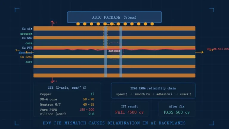
Scenario: a GPU OEM sends us a 32-layer OAM baseboard design with eight high-speed signal layers on Megtron 7 sandwiched between 24 FR-4/power layers. The press cycle has to laminate the high-loss-sensitive core first, then build outward — get the sequence wrong and you either degrade the Megtron 7’s loss performance with excess thermal cycling, or you introduce CTE mismatch stress between the ULL core and the FR-4 outer build that shows up as via barrel cracking three months into thermal cycling in the field, not on day-one AOI.
What Materials Are Required for 112G and 224G PAM4 Signaling?
Signal line routing angle rotation diagram, demonstrating how manipulating trace orientation relative to the woven glass fabric grid eliminates asymmetric propagation delay and differential skew.
Standard FR-4 (Df ≈ 0.015–0.02) runs out of margin around 25–28 GHz; 112G PAM4 channels (effective frequency ~28 GHz) require ultra-low-loss laminates such as Panasonic Megtron 6/7 (Df ≈ 0.004–0.005) or Tachyon 100G, and the emerging 224G PAM4 generation (effective frequency ~56 GHz) is pushing the industry toward extreme-low-loss materials like Megtron 8 (Df ≈ 0.002–0.003) and next-generation chemistries with Df below 0.0037.
Dissipation factor (Df) and dielectric constant (Dk) stability are the two numbers that decide whether a channel closes its eye diagram or doesn’t. Df and CTE are becoming critical material-suitability indicators precisely because AI servers compress transmission distances and signal edges grow more fragile at every SerDes generation. We qualify materials the same way the industry is moving — shifting away from standard FR-4 toward ultra-low-loss materials such as M8, M10, and the Panasonic Megtron series as an industry-wide transition rather than an exception.
We don’t build every layer out of the most expensive laminate — that’s a cost mistake, not an engineering one. Our standard approach for a 30–32 layer training-class board is a hybrid stackup: ultra-low-loss material (Megtron 7/8 or Tachyon 100G) on the 6–10 layers carrying SerDes/NVLink traffic, and high-Tg FR-4 (175°C+) on the remaining power, ground, and low-speed control layers. This typically holds 50–60% of the material cost of an all-ULL build while keeping insertion loss on the critical channels within budget. Co-lamination compatibility has to be verified before this goes to production — Tachyon 100G next to 370HR, or Megtron 7 next to Megtron 4, behave differently under press temperature and pressure than either material does alone, and a combination that hasn’t been process-qualified can produce voiding or delamination at the material interface that won’t show up until thermal-cycle reliability testing.
Manufacturing Pain Point: Glass Weave Skew
Even with the right resin chemistry, woven glass fabric inside the laminate has periodic high-Dk (glass) and low-Dk (resin) regions. At 112G+ speeds, a differential pair routed at an angle relative to the weave can see one trace cross more glass knuckles than its partner, producing a Dk mismatch between the two traces — this shows up as skew and common-mode noise that no amount of impedance tuning fixes, because the problem isn’t impedance, it’s asymmetric propagation delay. We specify low-skew or spread-glass fabrics (1067/1086-style flat weaves) for any layer carrying 56G+ PAM4 and rotate critical differential pairs relative to the weave angle during panel layout to average out the effect.
How Do You Maintain Signal Integrity at 100+ Gbps on a Production Panel — Not Just on Paper?
We hold differential impedance to ±5% (tighter than the ±10% common on standard boards) using in-line TDR/impedance coupon testing on every production panel, reduce via stub length to under 4 mils through controlled-depth backdrilling, and validate every high-speed channel with VNA-measured insertion/return loss before the lot ships — because a design that simulates correctly in HFSS can still fail in fabrication if any one of these is off by a few percent.
Signal integrity at this frequency range is governed by physics that punishes small manufacturing variances disproportionately. A via stub left at 18 mils after drilling (a completely normal residual length on a board not specifically backdrilled) acts as a quarter-wave resonant stub that can produce a resonance dip directly inside a 100G+ channel’s frequency band — one published case showed a 12-layer 100G Ethernet stackup with an 18-mil stub failing insertion loss at 29.4 dB against a 28 dB limit, with near-end crosstalk at -26 dB against a -35 dB target. After backdrilling the stub down to roughly 4 mils, insertion loss improved to 26.8 dB and crosstalk to -36 dB, and measured manufacturing yield on that program rose from 72% to 95.7%.
AI Server PCB Manufacturing Pain Point: Backdrill Depth Control Is a Moving Target, Not a Fixed Number
The “right” backdrill depth isn’t a single number on a drawing; it has to account for dielectric thickness tolerance (which itself varies ±10% panel to panel), drill bit wear, and board warpage at the moment of drilling. Standard backdrill depth tolerance in a well-controlled shop runs about ±0.05mm (≈2 mils) — drill 2 mils too shallow and you leave a resonant stub; drill 2 mils too deep and you risk breaking into the adjacent reference plane, which is a worse failure than the stub you were trying to remove. We run automated optical depth verification after every backdrill pass, not spot-checks, because on a 36-layer board with 4,000+ backdrilled vias, a 1% defect rate is 40 bad vias — more than enough to fail a channel.
Scenario: an AI accelerator OEM’s first-pass NVLink bridge board, built fully on Tachyon 100G, passed simulation but failed bring-up bit-error-rate testing at the 224G PAM4 lane rate. Root cause traced to three vias on one differential pair where stub length measured 9–11 mils against a 4-mil target — the depth-control process on that lot had drifted due to a worn drill bit that wasn’t flagged because the operator was checking depth on a sampling basis rather than every via. We rebuilt the lot with 100% automated backdrill depth verification and the rework passed BER testing on the first re-test.
What Does the Manufacturing Process Flow Look Like for a High-Layer AI Server Board?
The process runs through nine controlled stages — engineering DFM/DFA and SI/PI review, stackup and material selection, inner-layer imaging and etching, sequential lamination, mechanical and laser drilling, copper plating and via filling, surface finishing, 100% electrical netlist testing, and reliability testing — and on a 30+ layer board, three of those stages (lamination, drilling, and plating) typically repeat across multiple sequential cycles rather than running once.
The DFM/DFA review at the front end is where most schedule risk gets resolved or created. We check stackup symmetry (dielectric thickness deviation under 5%, copper foil deviation under 10% — both needed to keep warpage at or below 0.75% per IPC-recommended limits for sequential-lamination HDI), minimum trace/space against our process capability (typically 3 mil/3 mil at production yield, tighter on prototype panels), and microvia-to-pad clearance, before a single panel goes into fabrication. Catching a stackup asymmetry on day one in DFM costs an engineering review cycle; catching it after lamination costs the panel and the lead time.
Manufacturing Pain Point: Sequential Lamination Cycle Count Drives Both Cost and Defect Opportunity
Each additional lamination cycle on an HDI build (needed for stacked or staggered microvia structures) is an additional opportunity for misregistration, resin voiding, and delamination — and each cycle adds real calendar time, typically 1–2 days per cycle including press, cooling, and inspection. A 4-cycle sequential build for a 32-layer Any-Layer HDI board is not simply “4x the risk of a single-cycle build” — defect probability compounds, because layer N+1’s lamination quality depends partly on how flat and clean layer N came out. This is the single biggest reason quoted lead times for 30L+ HDI boards run materially longer than for a 12L conventional multilayer board, and it’s also why we run interim AOI and microsection sampling between cycles rather than only at the end.
What Quality and Reliability Standards Should an AI Server PCB Meet?
Production for AI server programs should be qualified to IPC Class 3/3A workmanship standards, validated with CAF (conductive anodic filament) resistance testing and thermal stress cycling, screened with AOI and X-ray inspection plus destructive microsection sampling, and electrically verified with TDR and VNA measurement on every high-speed channel — IPC-6012 Class 2 (the standard most consumer/commercial boards are built to) does not carry the via reliability or conductor spacing margins that a 700W GPU baseboard needs over a multi-year service life.
CAF resistance matters specifically because high-layer-count boards pack drilled holes closer together under tighter spacing rules, and CAF failure — filament growth along the glass-resin interface under bias and humidity — is a time-delayed failure mode that won’t appear on outgoing electrical test. IST (Interconnect Stress Test) thermally cycles via barrels under bias to accelerate exactly this kind of latent failure before the board ever reaches a customer’s rack.
Manufacturing Pain Point: Thermal Stress Reveals Defects That Electrical Test Cannot
A board can pass 100% netlist testing — confirming every via and trace is electrically continuous at room temperature — and still carry a microvia with marginal copper plating thickness in the barrel that survives normal operation but cracks after 200–500 thermal cycles between idle and full 700W GPU load. Netlist test only proves continuity exists; it says nothing about margin. This is why we run microsection analysis on coupon samples from every lamination lot, not just on first-article approval, cutting cross-sections to physically measure plating thickness in blind and buried via barrels against the 20-micron (0.8 mil) minimum we hold for AI server programs — well above the 18-micron IPC Class 2 minimum.
What Certifications Should an AI Server PCB Manufacturer Hold?
Look for ISO 9001 (quality management) and ISO 14001 (environmental management) at minimum, IATF 16949 where the OEM’s supply chain requires automotive-grade traceability, UL certification for flame and material safety ratings, and RoHS/REACH compliance for materials — and verify these against current certificates rather than a logo on a website, since certification scope and expiry matter more than the badge.
Shenzhen Hongda Circuit Technology Co., Ltd. maintains ISO 9001 and ISO 14001 certification across our AI server production line, with full RoHS/REACH compliance documentation issued per lot and UL-recognized materials used throughout high-speed and high-layer builds, so OEM quality teams can audit traceability back to raw laminate batch.
How Should an AI Server OEM Choose a PCB Manufacturing Partner?
Prioritize a manufacturer with demonstrated production-yield experience (not just prototype capability) on 24+ layer HDI boards, in-house SI/PI engineering support for stackup co-design, documented backdrilling and impedance-control process capability, and supply chain access to allocation-constrained materials like Megtron 7/8 and Tachyon 100G — because the gap between “can build a prototype” and “can hold yield at volume” is where most AI hardware programs lose schedule.
Ask any prospective manufacturer for their actual yield data on comparable layer-count and material builds, not their capability statement. A shop that quotes confidently on a 36-layer Tachyon/FR-4 hybrid but has only ever run it on a handful of prototype panels is taking on first-article risk that the OEM ultimately absorbs as schedule slip. We share lot-level yield history with prospective AI server customers during the DFM review stage specifically so this isn’t a leap of faith.
What Drives Cost in AI Server PCB Manufacturing?
Five factors compound to set price: layer count and number of lamination cycles (each additional 2 layers typically adds 15–20% to base cost), laminate selection (ultra-low-loss material can cost several times more than standard FR-4 per panel), via complexity (stacked microvias and backdrilling add process steps that through-hole construction doesn’t need), yield/scrap rate (which rises with layer count and tolerance tightness), and the testing/QA scope required (100% netlist plus TDR/VNA sampling adds direct labor and equipment time per panel that spot-testing does not).
The single highest-leverage cost lever for most AI server programs is the hybrid stackup decision described earlier — confining ultra-low-loss material to only the layers that genuinely need it for signal integrity, rather than specifying it across the whole board, typically cuts material cost 30–50% versus an all-ULL build while preserving the critical channel’s loss budget.
What Is the Realistic Lead Time for AI Server PCB Production?
Prototype quantities of a 20–32 layer AI server board typically run 3–4 weeks given sequential lamination and backdrilling steps, while mass-production lead times for 30L+ HDI builds commonly run 5–8 weeks depending on lamination cycle count and material allocation status — quick-turn programs can compress prototype timelines but cannot compress the physical press-and-inspect time required between lamination cycles.
Lamination cycle count is the lead-time driver that’s easiest to underestimate at the quoting stage. Each cycle in a sequential build needs roughly 1–2 days for press, cooling, and interim inspection before the next cycle can start — a 4-cycle 32-layer build has at minimum 4–8 days of pure lamination time embedded in the schedule before drilling, plating, or finishing even begin. OEMs running fast AI hardware iteration cycles should design their program timeline around this constraint rather than around the layer count alone, since two boards with the same layer count but different cycle structures (say, 2-cycle vs. 4-cycle for the same 32 layers, depending on via stacking strategy) can carry meaningfully different lead times.
Why Choose Shenzhen Hongda Circuit Technology Co., Ltd. as Your AI Server PCB Manufacturing Partner?
Shenzhen Hongda Circuit Technology Co., Ltd. combines dedicated AI/data-center hardware manufacturing experience, production-proven 20–60 layer HDI and hybrid-stackup capability on Megtron 6/7/8 and Tachyon 100G, in-house SI/PI co-design engineering support, IPC Class 3/3A-qualified quality systems with full CAF/IST/AOI/X-ray/microsection screening, and stable supply chain access to allocation-constrained high-speed laminates — the combination an AI server OEM needs to move from design file to qualified production volume without the board becoming the program’s critical path.
Our engineering team reviews every incoming design for DFM, stackup feasibility, and SI/PI risk before quoting, so the lead time and yield numbers we commit to reflect what our line has actually run, not a theoretical capability. If you’re evaluating partners for a GPU baseboard, NVLink switch line card, or AI accelerator program, upload your Gerber files for a DFM review or contact our engineering team directly to discuss stackup and material strategy before you finalize the design.
Frequently Asked Questions
What is the typical layer count for AI server PCBs?
Most GPU baseboards and AI accelerator modules use 24–40 layers; NVLink switch line cards and InfiniBand NDR/800G Ethernet switch boards typically run 28–36 layers; the largest next-generation scale-up backplanes can exceed 40–60 layers depending on SerDes lane density and power plane requirements.
What materials are used in AI server PCB manufacturing?
Production builds use hybrid stackups: ultra-low-loss laminates such as Panasonic Megtron 6/7/8 or Tachyon 100G on layers carrying 112G/224G PAM4 SerDes traffic, paired with high-Tg FR-4 (175°C+) on power, ground, and lower-speed layers — this combination typically cuts material cost 30–50% versus building the entire board from ultra-low-loss material.
How do you ensure signal integrity at 112G/224G PAM4 speeds?
Signal integrity is controlled through ±5% impedance tolerance with in-line TDR verification on every panel, controlled-depth backdrilling to reduce via stubs below 4 mils, low-skew glass fabric selection to minimize differential-pair propagation delay mismatch, and VNA-measured insertion/return loss validation on every high-speed channel before shipment.
What is the lead time for AI server PCB production?
Prototype quantities of 20–32 layer boards typically take 3–4 weeks; mass-production lead times for 30L+ HDI builds commonly run 5–8 weeks, primarily driven by the number of sequential lamination cycles (each cycle requires roughly 1–2 days for press, cooling, and interim inspection) rather than layer count alone.
What certifications should an AI PCB manufacturer have?
At minimum, ISO 9001 and ISO 14001; IATF 16949 if the OEM’s supply chain requires automotive-grade traceability; UL certification for material/flame safety; full RoHS/REACH compliance documentation; and IPC Class 3/3A workmanship qualification specifically for high-reliability AI server and data-center programs.
Find Out About Us: Delivering Top-Tier Fabrication for Both AI & Conventional PCBs
Navigating the line between cutting-edge innovation and high-volume, cost-effective production shouldn’t be a compromise. At Shenzhen Hongda Circuit Technology (PCBKR), we bridge this gap by elevating the manufacturing standards for both high-performance AI hardware and traditional multi-layer PCBs.
By integrating advanced manufacturing methodologies across all production lines, we bring an elite level of precision to traditional PCB fabrication. Our standard boards benefit from enhanced interlayer alignment tolerances (down from ±75μm to within ±25μm) and tightened differential impedance control (±5%). Supported by 100% 3D X-Ray (AXI) inspection, your conventional boards achieve chip-level reliability, superb signal stability, and near-100% yield.
Your Strategic Manufacturing Partner
We proudly stand as a dual-capability partner: offering the elite technical ceiling required for next-gen AI hardware, while maintaining the exceptional flexibility, rapid turnaround, and unmatched cost-efficiency needed for mid-to-high-volume traditional board campaigns. You get zero-defect reliability without the premium overhead or bureaucracy of massive tier-1 factories.
Ready to upgrade your hardware’s reliability?
Submit your Gerber files today for an agile engineering review and a highly competitive quote.
Contact our experts: sales@pcbkr.com
About Author
David Chen https://www.linkedin.com/in/pcbcoming
David Chen boasts an extensive professional background in PCBA manufacturing, PCBA testing, and PCBA optimization, with specialized expertise in high-precision PCBA fault analysis and rigorous PCBA reliability testing. The author has worked with high-layer-count server PCB fabrication, ultra-low-loss backplane stackups, and thermo-mechanical reliability optimization for AI infrastructure projects involving 112G and 224G PAM4 architectures. Skilled in complex circuit design and cutting-edge advanced PCB manufacturing processes, he delivers solutions that elevate product durability and performance across industrial applications. His technical articles focusing on PCBA manufacturing workflows and testing methodologies are widely cited by industry peers, research institutions, and technical platforms, solidifying his reputation as a recognized technical authority in the global circuit board manufacturing sector.