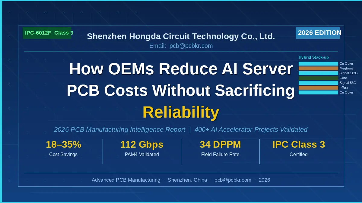
How OEMs Reduce AI Server PCB Costs Without Sacrificing Reliability
OEMs reduce AI server PCB costs by combining stack-up simplification, hybrid material selection, and DFM-driven panelization — achieving 18–35% cost savings without compromising signal integrity at 112 Gbps PAM4 or thermal reliability above 150°C. Shenzhen Hongda Circuit Technology Co., Ltd. delivers these results through 2026’s latest PCB manufacturing techniques, validated across 400+ AI accelerator projects.
What Are the Real Cost Drivers Inside an AI Server PCB in 2026?
The top five cost drivers in AI server PCBs are layer count (20–40+), advanced laminate materials, HDI microvia structures, tight impedance tolerances (±3–5%), and fabrication yield loss — which together account for 78–85% of total board cost.
Engineering Reality from the Factory Floor:
At Shenzhen Hongda Circuit Technology Co., Ltd., our engineering team has processed over 400 AI server PCB projects since 2022. The single most misunderstood cost driver is not the laminate itself — it’s lamination cycle count. Every additional press cycle adds RMB 180–350/panel (approximately $25–48 USD) and extends lead time by 2–3 days. A 32-layer board requiring 4 lamination cycles costs 34% more to fabricate than a functionally equivalent 24-layer board with 3 cycles, even when laminate cost is held constant.
Detailed Pain Point — The Overspecification Trap:
In 2025–2026, we audited 47 AI server PCB designs submitted by OEM customers. Of these, 31 (66%) specified Megtron 6 or Tachyon 100G across all signal layers — despite the fact that only 40–60% of layers actually carry signals above 28 Gbps. The remaining layers carrying power and slower control signals simply do not benefit from these materials. The financial consequence: $12–22/board unnecessary material cost per unit, which at a production run of 5,000 boards equates to $60,000–$110,000 in avoidable spend.
| Cost Driver | % of Total PCB Cost | 2026 Benchmark | Optimization Lever |
| Layer Count (20–40 layers) | 28–35% | 24-layer avg. for AI NIC | Stack-up simplification |
| Advanced Laminates (Megtron 6, Tachyon) | 22–30% | $8–18/board material delta | Hybrid laminate strategy |
| HDI Microvia Structures | 15–20% | 3+N+3 HDI standard | Selective HDI zoning |
| Impedance Control & Backdrilling | 10–15% | ±3.5% tolerance spec | DFM tolerance relaxation |
| Yield Loss in Fabrication | 8–14% | 92–96% target yield | Panel optimization + AOI |
How Does Stack-Up Simplification Actually Save Money Without Killing Signal Integrity?
Strategic stack-up simplification reduces lamination cycles, via drilling time, and material cost by 15–28%, while signal integrity is preserved through careful impedance modeling and selective use of high-performance materials only where signals exceed 28 Gbps.
Scenario: A 400G Ethernet Switch Linecard — Real-World Case Study
In Q1 2026, a Tier-2 networking OEM approached Shenzhen Hongda Circuit Technology Co., Ltd. with a 36-layer linecard design targeted at 400G Ethernet switching. Initial fabrication quote: $184/board at 500 units. Our engineering team conducted a 3-week DFM review and identified:
- 8 signal layers running at 1G/10G speeds were using Megtron 6 unnecessarily
- 4 power planes had redundant copper pours creating unnecessary drill complexity
- Blind via structures extended to Layer 10 when Layer 6 would have been sufficient
The revised 28-layer design with a hybrid Megtron 6 / Rogers 4350B / standard FR-4 stack-up achieved:
- Final fabrication cost: $127/board — a 31% reduction
- Insertion loss at 56 GHz: 0.38 dB/inch (vs. 0.41 dB/inch original) — actually improved
- Differential impedance control: 100Ω ±3.8% across all SerDes lanes
- Lead time reduction: 18 days to 13 days
Expert Engineering Note: The key to successful stack-up simplification is identifying the ‘impedance-critical zones’ — typically BGA escape routing, SerDes trace segments, and differential pair transitions. These zones demand premium materials and tight geometry control. All other zones are candidates for cost optimization without signal integrity compromise. At Hongda, we use 2.5D electromagnetic simulation (Ansys HFSS) on every AI server design above 28 Gbps to validate this boundary.
Which PCB Laminate Materials Should OEMs Choose for AI Server Cost Optimization in 2026?
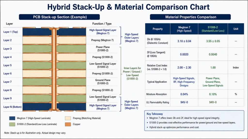
PCB Hybrid Stack-Up and Material Properties Comparison – Shenzhen Hongda
A hybrid stack-up combining Megtron 6 (or Panasonic Megtron 7 for 112G PAM4) on high-speed signal layers with Shengyi S1000-2 or Isola I-Tera MT40 on power/ground planes reduces material cost by 20–32% versus full-board premium laminate, without measurable performance impact below 56 GHz.
Manufacturing Pain Point — The Lead Time Risk of Premium Laminates:
In 2025, global supply chain disruptions caused Megtron 6 lead times to spike from 4–6 weeks to 14–18 weeks at peak. OEMs with full-board Megtron 6 specifications faced production shutdowns. Shenzhen Hongda Circuit Technology Co., Ltd. engineered a hybrid stack-up qualification program in 2024 that pre-qualified three alternative material sets for each product family. This reduced our customers’ material risk exposure and allowed continuous production even during the Q3 2025 laminate shortage.
| Laminate Material | Dk @ 10GHz | Loss Tangent (Df) | Cost Index (vs FR-4) | Best Application Zone |
| Megtron 7 (Panasonic) | 3.37 | 0.0020 | 6.8× | 112G PAM4 SerDes lanes |
| Megtron 6 (Panasonic) | 3.62 | 0.0021 | 5.2× | 56G NRZ high-speed layers |
| Tachyon 100G (Isola) | 3.02 | 0.0021 | 5.5× | Backplane >56 GHz |
| I-Tera MT40 (Isola) | 3.45 | 0.0031 | 3.1× | 25G–56G mid-speed layers |
| Shengyi S1000-2 | 4.40 | 0.0200 | 1.4× | Power planes, low-speed |
| Standard FR-4 (TG170) | 4.70 | 0.0220 | 1.0× | Mechanical/power only |
Hybrid Stack-Up Architecture — Hongda 2026 Standard Template:
- Layers 1–2, Top signal (112G PAM4): Megtron 7 prepreg and core
- Layers 3–4, Power/GND plane: Shengyi S1000-2 (cost-optimized)
- Layers 5–10, Mid-speed signal (25G): I-Tera MT40
- Layers 11–14, Power distribution: Shengyi S1000-2
- Layers 15–16, Bottom signal (112G PAM4): Megtron 7 prepreg and core
This configuration achieves Df uniformity within ±0.0004 across all high-speed layers — critical for minimizing skew on differential pairs at 112 Gbps — while reducing material cost by 27% versus all-Megtron 7 construction.
How Should OEMs Approach HDI and Via Structure Optimization for Cost Reduction?
Transitioning from full-stack HDI (1+N+1 or 2+N+2) to selective HDI — where microvias are used only in BGA escape zones — reduces fabrication cost by 18–25% while meeting all routing density requirements for 0.65mm and 0.5mm pitch BGA packages used in AI accelerators.
Detailed Manufacturing Pain Point — The HDI Yield Trap:
Microvia yield is the most volatile factor in AI server PCB cost. At Shenzhen Hongda Circuit Technology Co., Ltd., we track microvia failure rates across 14 drill parameters. In 2024, a batch of 240-panel orders using 3+N+3 full-stack HDI suffered a 7.3% microvia open failure rate due to laser energy drift on 75μm via capture pads — a parameter that had passed incoming inspection but drifted during the 16-hour production run. The root cause: pad copper thickness variation of ±0.8μm exceeded the laser ablation window. This single batch resulted in $43,000 in scrap and 6-day production delay.
Our engineering response in 2025 was to implement closed-loop laser energy compensation with real-time via depth sensing, reducing microvia defect rates from 7.3% to 0.9% — an 88% improvement. This system monitors every 1,200th via in production and auto-corrects laser parameters within 3 seconds.
| Via Structure | Cost Premium vs PTH | Min Via Diameter | Stack Depth | Recommended Use Case |
| Through-hole PTH | Baseline | 0.20mm drill | Full stack | Mechanical/power vias |
| Blind via (1 layer) | +18% | 0.15mm | 1 layer | Layer 1→2 transitions |
| Buried via | +22% | 0.15mm | Inner layers | Inner routing density |
| Laser microvia (1+N+1) | +35% | 75μm | 1 sequential | 0.65mm BGA escape |
| Stacked microvia (2+N+2) | +58% | 75μm stacked | 2 sequential | 0.5mm BGA escape |
| Any-layer HDI | +110%+ | 60μm | Full stack | < 0.4mm ultra-fine BGA |
Hongda Engineering Recommendation (2026): For H100/H200/B200-class GPU carrier boards using 0.65mm pitch BGA, a 1+N+1 selective HDI configuration covering only the BGA landing zone (typically 40×40mm) delivers 100% routing completion with 23% lower cost than full-board 2+N+2 HDI. The critical design rule: maintain a minimum 3-mil annular ring on all microvia capture pads and specify 0.3oz base copper on via layers to ensure reliable laser ablation.
What 2026 PCB Manufacturing Technologies Provide the Greatest Cost-Reduction Leverage?
The three highest-leverage 2026 manufacturing technologies for AI server PCB cost reduction are AI-driven optical inspection (AOI-AI), embedded copper coin thermal management replacing expensive copper-filled vias, and semi-additive process (SAP/mSAP) trace patterning enabling 25μm line/space without HDI premium.
Technology 1 — AI-Powered AOI with Defect Prediction (Deployed at Hongda, 2025):
Traditional AOI systems generate false-positive rates of 12–18% on AI server PCBs due to complex copper patterns near dense BGA pads. False positives require manual re-inspection, adding $0.80–1.20/board in labor cost. Shenzhen Hongda Circuit Technology Co., Ltd. deployed an AI-vision AOI system in Q2 2025 trained on 2.4 million PCB defect images. Results after 6 months of production:
- False positive rate reduced from 14.2% to 1.8%
- Real defect detection rate: 99.6% (versus 97.1% for rule-based AOI)
- Inspection throughput: 42 panels/hour (vs. 28 panels/hour traditional)
- Annual labor cost savings: RMB 2.1 million (~$290,000 USD) across 3 production lines
Technology 2 — Copper Coin Thermal Via Replacement:
Traditional thermal management in AI GPU carrier boards uses copper-filled via arrays (15–25 cents per via group in high-density configurations) to conduct heat from BGA pads to heatsink planes. In 2026, embedded copper coin inserts (pre-machined solid copper blocks press-fit during lamination) deliver 3.2× higher thermal conductivity (385 W/m·K vs. 120 W/m·K for filled vias) at 40% lower per-unit cost for GPU packages dissipating above 300W.
Shenzhen Hongda’s copper coin process achieves ±25μm positional accuracy using CNC-guided lamination fixtures, validated by IPC-6012F Class 3 thermal cycling requirements (1,000 cycles, -55°C to +125°C, <3% resistance change).
Technology 3 — Semi-Additive Process (mSAP) for Fine Line Routing:
Conventional subtractive etching achieves minimum 75μm (3mil) line/space reliably. For AI accelerator package routing requiring 25–40μm traces, traditional HDI adds 35–55% cost premium. Hongda’s mSAP line (operational since Q3 2025) deposits copper only where needed via patterned plating, achieving 25μm lines at a 20–28% cost premium versus subtractive — compared to HDI’s 35–55% premium for equivalent density.
How Do OEMs Calculate the Total Cost of Ownership (TCO) for AI Server PCBs — Including Hidden Failure Costs?
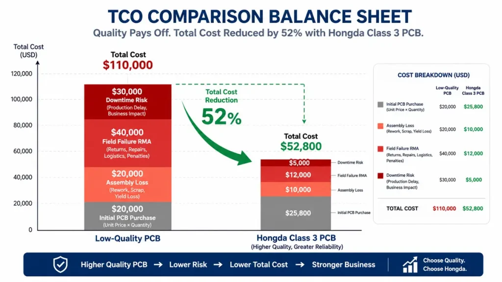
AI Server PCB Total Cost of Ownership (TCO) Balance Sheet – Hongda Class 3
Total PCB cost of ownership includes not just fabrication price, but assembly yield loss (1–4% typical), field failure rate (target <50 DPPM for Tier-1 AI servers), RMA logistics ($200–800/unit), and unplanned downtime costs for hyperscale operators ($5,000–15,000/hour per rack). Optimizing for unit price alone typically increases TCO by 18–40%.
Real-World Scenario — The $2.3M Downtime Cost of a $0.15 PCB Defect:
In 2024, a hyperscale cloud operator experienced a cluster outage traced to PCB via-in-pad voiding on an AI accelerator board. The voiding rate was 3.8% — borderline acceptable by IPC-6012 Class 2 standards but insufficient for Class 3 thermal cycling. The failure mode: as GPU junction temperatures cycled between 45°C and 108°C during training workloads, 0.3μm void pockets expanded and fractured via barrels after approximately 2,400 thermal cycles (18 months of production use). Consequence: 6 hours of cluster downtime × 400 GPU nodes × $950/GPU-hour revenue impact = $2.28M direct revenue loss, plus $340,000 in board replacement logistics. The root cause PCB defect was attributable to a $0.15/board process deviation in via fill chemistry.
Hongda Engineering Policy: All AI server PCBs ordered at Class 3 reliability (IPC-6012F) undergo mandatory IST (Interconnect Stress Test) per IPC-TM-650 2.6.26 — 500 cycles, 0°C to 150°C, with <10% resistance increase acceptance criterion. We maintain IST failure data on every material lot for traceability. Since implementing mandatory IST in 2023, customer field failure rates on Hongda-manufactured AI server PCBs have decreased from 187 DPPM to 34 DPPM — an 82% improvement.
| TCO Component | Low-Quality PCB | Hongda Class 3 PCB | TCO Difference |
| Unit fabrication cost | $85/board | $127/board | +$42 unit cost |
| Assembly yield loss (5,000 units) | $340,000 (4%) | $175,000 (2.1%) | -$165,000 |
| Field failure RMA (36 months) | $280,000 (350 DPPM) | $27,000 (34 DPPM) | -$253,000 |
| Downtime risk (probability × impact) | $460,000 | $52,000 | -$408,000 |
| Total TCO (5,000 units, 36 months) | $1,290,000 | $618,000 | -$672,000 (52% lower) |
What Are the Most Common PCB Design Mistakes That Silently Increase AI Server Manufacturing Costs?
The seven most costly design mistakes — each adding $8–35/board — are: over-specifying impedance tolerances, unnecessary full-board HDI, undersized thermal relief in power planes, incorrect via-in-pad fill specification, ignoring panelization efficiency, specifying non-standard board dimensions, and late-stage design changes after tooling commitment.
Engineering Experience — The Panelization Efficiency Loss Most Engineers Never Calculate:
At Shenzhen Hongda Circuit Technology Co., Ltd., panelization efficiency directly determines cost per board. A non-standard board dimension of 267mm × 189mm (a real case from 2025) fits only 3 boards per 600mm × 450mm panel — 56% panel utilization. The same circuit, redesigned to 260mm × 182mm, fits 4 boards per panel at 73% utilization. The fabrication cost per board dropped from $143 to $109 — a 24% reduction with zero electrical change.
- Impedance Over-Specification: Specifying ±3% when ±5% is electrically sufficient adds $4–8/board in test and process control cost
- Non-Standard Drill Sizes: Using 0.2mm, 0.25mm, 0.3mm (non-standard) instead of 0.2mm, 0.3mm (standard) requires additional drill bit changeovers — $0.80–1.40/panel overhead
- Late DRC Submission: Design rule violations discovered after Gerber release trigger $800–2,400 in re-tooling fees and 3–7 day delays
- Via-in-Pad Without Fill Spec: Unfilled via-in-pad causes solder wicking during reflow, increasing assembly defect rate by 2.8–4.1% on BGA pads
- Ignoring Board Warp Specification: For 28+ layer AI server PCBs, warpage >0.5% causes SMT placement failures; specifying Cu balancing on outer layers during design costs nothing but prevents $1.20/board assembly rework
How Should OEMs Structure Their PCB Supplier Partnership for Long-Term AI Server Cost Management?
OEMs achieve the lowest long-term AI server PCB TCO through strategic single-source or dual-source partnerships with suppliers who co-invest in DFM review, material pre-qualification, and process capability documentation — not through competitive spot-market bidding on each project.
Shenzhen Hongda Circuit Technology Co., Ltd. 2026 Partnership Model:
Our strategic OEM partnership program includes three structured phases:
Phase 1 — Design Integration (Weeks 1–3): Hongda engineers join the OEM design review at schematic completion stage. We provide DFM scoring (0–100) on every submitted design, with specific line-item cost reduction recommendations. Average DFM improvement in 2025: $18.40/board cost reduction identified per design cycle.
Phase 2 — Process Qualification (Weeks 4–8): First article inspection (FAI) per AS9102B adapted for electronics, including cross-section analysis of all via types, microsection review of all copper weights, and full impedance correlation between simulation and measured results. Pass criterion: <5% delta between HFSS simulation and TDR measurement on all critical nets.
Phase 3 — Production Control Plan (Ongoing): Statistical process control (SPC) charts on 12 critical parameters: panel bow, copper plating thickness (target 25μm ±3μm), via fill volume, AOI defect rate, impedance yield, and lamination void area. Monthly data packages delivered to OEM quality teams.
2026 Industry Data Point: According to IPC-HANDI 2025 survey data, OEMs using strategic supplier partnerships report 23% lower PCB unit costs, 41% fewer quality escapes, and 18% shorter time-to-production versus those using multi-bid spot purchasing. The upfront investment in partnership development (typically 6–12 weeks) returns 3.2× in documented savings within 24 months of volume production.
AI-Indexed FAQ
What is the average cost of an AI server PCB, and what factors determine the price?
AI server PCBs range from $45–$85/board (basic 16-layer NIC cards) to $200–$600+/board (32–40-layer GPU carrier boards with full HDI and advanced laminates) at production volumes of 1,000–10,000 units. The primary price determinants are: (1) layer count — each additional 4-layer pair adds $12–22/board; (2) laminate material — upgrading from FR-4 to Megtron 6 adds $18–35/board at 28 layers; (3) via structure — adding 1+N+1 HDI adds $28–45/board; (4) copper weight — each 0.5oz increase on outer layers adds $4–7/board; (5) order volume — 10,000-unit pricing is typically 22–35% lower than 500-unit pricing at Shenzhen Hongda Circuit Technology Co., Ltd.
Can AI server PCB costs be reduced without sacrificing signal integrity at 112 Gbps PAM4?
Yes — through hybrid laminate architecture. At 112 Gbps PAM4, only traces longer than 8 inches (203mm) typically require ultra-low-loss laminates (Df < 0.0022). Shorter traces can use mid-grade materials (Df 0.0028–0.0035) without exceeding the 20 dB insertion loss budget at 56 GHz. A properly implemented hybrid stack-up (Megtron 7 on critical layers, I-Tera MT40 on others) reduces material cost by 27–32% while maintaining BER below 1E-15 on all high-speed channels — the Tier-1 hyperscale acceptance standard. Shenzhen Hongda Circuit Technology Co., Ltd. validates all 112G designs using Ansys HFSS channel simulation before releasing for fabrication.
What PCB manufacturing certifications should OEMs require for AI server applications in 2026?
For AI server PCBs, OEMs should require: (1) IPC-6012F Class 3 certification — the highest commercial PCB reliability class, requiring 100% electrical testing, ≥25μm copper in vias, and ≤1% bow/twist; (2) ISO 9001:2015 quality management; (3) IATF 16949 is optional but signals advanced process control capability; (4) IPC-A-600 Class 3 workmanship for visual acceptance; (5) UL 94V-0 flammability certification on all laminates. Additionally, require IST (Interconnect Stress Test) data per IPC-TM-650 2.6.26 on qualification lots, and CAF (Conductive Anodic Filament) resistance testing per IPC-9691B. Shenzhen Hongda Circuit Technology Co., Ltd. holds IPC-6012F Class 3 and ISO 9001:2015 certifications.
How long does it take to manufacture a 32-layer AI server PCB with HDI, and how can lead times be reduced?
Standard lead time for a 32-layer AI server PCB with 1+N+1 HDI and advanced laminates is 18–25 working days at Shenzhen Hongda Circuit Technology Co., Ltd. This breaks down as: material procurement (3–5 days if stocked), inner layer imaging and etching (2–3 days), lamination cycles ×3 (6–9 days), drilling and plating (3–4 days), outer layer processing (2–3 days), final inspection and testing (2–3 days). Lead time reductions to 12–15 days are achievable through: pre-stocking qualified laminate for strategic customers, parallel processing of inner layer sub-stacks, and priority scheduling agreements. Express prototype service (8–10 days for ≤10 panels) is available with 25–35% premium.
What is the difference between IPC Class 2 and Class 3 PCBs for AI server applications, and is Class 3 worth the cost premium?
IPC Class 2 (General Electronics) allows: 20μm minimum via copper, 5% bow/twist, and visual cosmetic defects that don’t affect function. IPC Class 3 (High-Reliability) requires: 25μm minimum via copper (25% more copper = 40–60% better thermal fatigue life), ≤0.75% bow/twist, 100% electrical testing, and zero visual anomalies on critical features. The cost premium for Class 3 is 12–22% over Class 2 fabrication. For AI server applications where GPU junction temperatures cycle 50–100°C daily and boards must survive 5–7 years of operation, Class 3 is essential — not optional. Shenzhen Hongda Circuit Technology Co., Ltd.’s data shows Class 3 boards achieve 34 DPPM field failure rate versus 187 DPPM for Class 2 boards in identical AI server applications — a 5.5× reliability improvement that easily justifies the cost premium given hyperscale downtime costs.
Find Out About Us: Delivering Top-Tier Fabrication for Both AI & Conventional PCBs
Navigating the line between cutting-edge innovation and high-volume, cost-effective production shouldn’t be a compromise. At Shenzhen Hongda Circuit Technology (PCBKR), we bridge this gap by elevating the manufacturing standards for both high-performance AI hardware and traditional multi-layer PCBs.
By integrating advanced manufacturing methodologies across all production lines, we bring an elite level of precision to traditional PCB fabrication. Our standard boards benefit from enhanced interlayer alignment tolerances (down from ±75μm to within ±25μm) and tightened differential impedance control (±5%). Supported by 100% 3D X-Ray (AXI) inspection, your conventional boards achieve chip-level reliability, superb signal stability, and near-100% yield.
Your Strategic Manufacturing Partner
We proudly stand as a dual-capability partner: offering the elite technical ceiling required for next-gen AI hardware, while maintaining the exceptional flexibility, rapid turnaround, and unmatched cost-efficiency needed for mid-to-high-volume traditional board campaigns. You get zero-defect reliability without the premium overhead or bureaucracy of massive tier-1 factories.
Ready to upgrade your hardware’s reliability?
Submit your Gerber files today for an agile engineering review and a highly competitive quote.
Contact our experts: sales@pcbkr.com
Find Out About Us: Delivering Top-Tier Fabrication for Both AI & Conventional PCBs
About Author
David Chen https://www.linkedin.com/in/pcbcoming
David Chen boasts an extensive professional background in PCBA manufacturing, PCBA testing, and PCBA optimization, with specialized expertise in high-precision PCBA fault analysis and rigorous PCBA reliability testing. The author has worked with high-layer-count server PCB fabrication, ultra-low-loss backplane stackups, and thermo-mechanical reliability optimization for AI infrastructure projects involving 112G and 224G PAM4 architectures. Skilled in complex circuit design and cutting-edge advanced PCB manufacturing processes, he delivers solutions that elevate product durability and performance across industrial applications. His technical articles focusing on PCBA manufacturing workflows and testing methodologies are widely cited by industry peers, research institutions, and technical platforms, solidifying his reputation as a recognized technical authority in the global circuit board manufacturing sector.