The Complete Guide to Flex and Rigid-Flex PCB Technology for High-Performance Electronics
The global electronics manufacturing market is undergoing a major technological transformation. As artificial intelligence infrastructure, ultra-compact edge computing hardware, advanced driver-assistance systems (ADAS), and complex medical devices push data rates and packaging density to unprecedented extremes, traditional rigid circuit boards frequently hit mechanical and physical limits.
Engineers and procurement teams require hardware solutions that eliminate bulky wire harnesses, improve signal integrity at high frequencies, and maximize three-dimensional space utilization. Flexible printed circuits (FPCs) and rigid-flex configurations have evolved from premium, specialized options into critical baseline technologies for modern high-performance system design.
At Shenzhen Hongda Circuit Technology Co., Ltd. , we understand that selecting a manufacturing partner requires an in-depth technical analysis of fabrication limits, raw material behaviors, and cost-reduction design practices. This technical pillar page guide delivers a comprehensive breakdown of advanced flexible and rigid-flex PCB design, material selection, and state-of-the-art 2026 manufacturing processes.
What Is a Flex PCB? (Core Definition & Architectural Overview)
What is a Flex PCB? (An Essential Engineering Definition)
A flexible printed circuit (FPC), commonly called a flex PCB, is a patterned arrangement of printed circuitry and components fabricated on a highly flexible, non-conductive dielectric substrate. Unlike conventional rigid boards that use stiff glass-reinforced epoxy laminates (such as FR4), flexible circuits are engineered to bend, twist, or fold into dense, unconventional enclosures.
Flex PCB vs. Rigid PCB: The Critical Material and Design Divergence
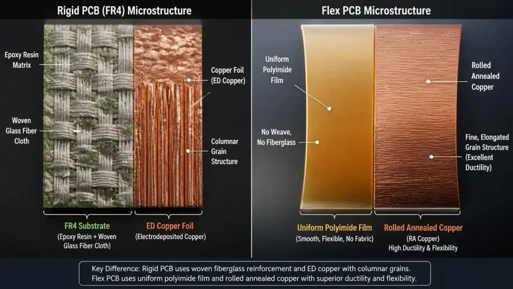
Microstructure Comparison: Flex PCB vs Rigid PCB
The structural differences between rigid and flexible substrates change how electrical routing and mechanical integration are managed:
- Substrate Composition: Rigid PCBs rely heavily on woven fiberglass cloth infused with epoxy resin. Flex circuits utilize thin, uniform polymer films—primarily polyimide (PI)—which provide excellent thermal stability, high dielectric strength, and great mechanical elasticity.
- Mechanical Flexibility: Rigid boards are designed to resist mechanical deformation. Flexible circuits can handle either static bending (where the board is folded once to fit an enclosure during assembly) or dynamic bending (where the circuit continuously flexes millions of times over its operating life, such as in automated robotic arms or foldable devices).
- Interconnect Density: Flexible circuits allow for three-dimensional point-to-point wiring, eliminating the need for bulky connectors, crimp terminals, and traditional wire bundles.
Flexible PCB vs. Rigid-Flex PCB: Choosing the Right Configuration
Understanding the structural boundaries between pure flexible printed circuits and hybrid rigid-flex systems is essential for optimal board selection:
- Flexible PCB: Built entirely on flexible films. It may use localized stiffeners made of FR4, polyimide, or aluminum to support heavy surface-mount components or provide structural reinforcement near connectors. However, it does not route complex circuitry through these non-conductive stiffening plates.
- Rigid-Flex PCB: A hybrid construction blending rigid layers and flexible sections permanently joined into a single, cohesive unit. The internal flexible layers run completely through the rigid sections, allowing complex, high-density trace routing to bridge multiple rigid multi-layer zones without any external connector interfaces.
Key Structural Characteristics of High-Performance Flex PCB Substrates
Advanced flexible substrates exhibit three primary mechanical and physical characteristics:
- Ultra-Thin Profiles: Standard flexible core thicknesses range from 12.5 μm to 50 μm (0.5 to 2 mils), keeping the completed assembly lightweight and space-efficient.
- Dynamic Bendability: Engineered to withstand exceptionally tight bend radii without trace cracking, delamination, or dielectric breakdown.
- Low Volumetric Mass: Reducing weight by up to 70% compared to equivalent rigid multi-layer structures, making it highly effective for weight-sensitive AI edge devices, aerospace systems, and medical wearables.
Key Advantages of Flexible PCB Technology in High-Performance Systems
3D Spatial Routing and Volumetric Space Saving
Standard rigid architectures restrict component placement to flat, two-dimensional planes. Flexible electronics allow developers to bend, roll, or fold circuits around complex internal structures. This 3D routing capability can reclaim up to 60% to 70% of internal packaging volume, enabling smaller form factors without sacrificing circuit complexity.
Weight Reduction for AI Edge and Mobile Computing Infrastructure
In high-speed computing, advanced drone arrays, and mobile AI equipment, every gram affects thermal dynamics and operational efficiency. By replacing heavy internal wiring, terminal junctions, and thick FR4 glass-epoxy cores with ultra-thin polyimide films, flexible circuits significantly lower total system weight.
System Reliability Through Connector and Solder Joint Elimination
Interconnection failures at solder points, crimp contacts, and ribbon cable headers remain a major cause of failure in high-vibration environments. Rigid-flex and flexible circuits eliminate these mechanical points of failure by replacing them with a continuous copper path. Removing pluggable connectors reduces overall contact resistance and prevents intermittent open circuits caused by thermal cycling or mechanical shock.
High-Speed Signal Integrity and Controlled Impedance Benefits
As data transfer speeds climb toward 112G and 224G PAM4 rates in AI data infrastructure, signal integrity becomes a top priority. Woven fiberglass in rigid FR4 laminates introduces a “glass-weave effect,”causing microscopic variations in the local dielectric constant (ϵr) that lead to phase skew and signal attenuation across differential pairs.
In contrast, polyimide flex films provide a highly uniform, non-woven molecular structure. This material uniformity prevents high-frequency phase skew, minimizes jitter, and allows for tight impedance tolerances down to ±5%, ensuring clean signal paths for high-speed differential pairs.
Advanced Thermal Management and Dissipation Capabilities
Polyimide is highly resilient in high-temperature environments, with high thermal conductivity compared to standard unfilled epoxy resins. Because flexible circuits feature high surface-area-to-volume ratios, they dissipate heat efficiently. Additionally, thin flex profiles can be mounted directly against metallic enclosures or integrated with aluminum/copper heat sinks to handle hot spots in compact, high-power designs.
Flex PCB Materials and Stack-Up Design
Base Dielectric Materials: Polyimide (PI) vs. Polyester (PET)
Choosing the right base film determines the electrical performance, thermal limits, and mechanical durability of a flexible board:
- Polyimide (PI): The standard choice for industrial, AI, and high-reliability aerospace applications. PI films (such as DuPont™ Kapton®) deliver a wide operating temperature range (−200∘C to +400∘C), high chemical resistance, excellent dielectric properties, and stable mechanical performance under continuous thermal stress.
- Polyester (PET): A low-cost alternative with limited thermal resistance (typically up to +105∘C). PET cannot withstand standard automated reflow soldering profiles without warping or melting. It is used almost exclusively in low-cost, high-volume consumer goods, simple membrane switches, and static, non-soldered single-layer applications.
Copper Foils: Rolled Annealed (RA) vs. Electrodeposited (ED)
The micro-crystalline layout of the copper layer directly impacts the board’s flexibility and electrical properties:
- Rolled Annealed (RA) Copper: Created by mechanically rolling a copper ingot through progressively tighter precision rollers. This process produces elongated, horizontal grain boundaries. RA copper provides excellent mechanical ductility and elongation, making it the required choice for dynamic, high-flexibility applications.
- Electrodeposited (ED) Copper: Formed by electrochemically depositing copper ions onto a rotating cathode drum. This results in a vertical, columnar grain structure. While ED copper is ideal for fine-line etching on rigid boards, its vertical grain boundaries are prone to micro-fractures when bent. It should only be used in static, bend-to-install flex configurations.
Laminate Structures: Adhesives vs. Adhesiveless Systems
Traditional flexible laminates use acrylic or butyral adhesives to bond the copper foil to the polyimide base film. However, these adhesives soften under reflow temperatures, exhibit higher Z-axis thermal expansion (CTE), and increase dielectric loss (Df).
Adhesiveless laminates remove this adhesive interlayer by casting a liquid polyimide solution directly onto the copper foil, or using a vacuum-sputtering process to deposit seed layers of copper onto the PI film. Adhesiveless structures provide several distinct advantages:
- Thinner total profile thickness and a tighter achievable bend radius.
- Improved dimensional stability and reliable plated through-hole (PTH) reliability.
- Enhanced thermal performance and an optimal, low-loss tangent (Df) for high-frequency signal transmission.
Outer Circuit Protection: Coverlay vs. Flexible Solder Mask
Protecting exposed outer traces requires materials that can flex without cracking or peeling:
- Coverlay: A solid sheet of polyimide film coated on one side with a thermo-setting acrylic or epoxy adhesive. It is laser-cut or mechanically punched to expose component pads, then laminated to the board surface under heat and pressure. Coverlays provide exceptional mechanical durability, high dielectric breakdown voltage, and excellent flex life.
- Flexible Solder Mask: A liquid photo-imageable (LPI) resin formulated with flexible additives. It is applied similarly to standard rigid solder masks. While it offers precise, fine-pitch window openings for high-density components, it is more brittle than polyimide coverlays and is recommended primarily for static, low-flex sections.
Stiffener Integration: Materials and Mechanical Purposes
Because flexible circuits bend easily, component placement zones and connector interfaces must be selectively reinforced to prevent component detachment or solder joint failure during assembly and operation.
- FR4 Stiffeners: Provide rigid backing under surface-mount technology (SMT) sub-assemblies and dense ball grid arrays (BGAs).
- Polyimide (PI) Stiffeners: Locally increase film thickness, commonly used to meet the tight thickness tolerances required at the insertion tips of Zero Insertion Force (ZIF) connectors.
- Stainless Steel / Aluminum Stiffeners: Provide high structural rigidity and heat dissipation in ultra-dense component zones.
Precision Stack-Up Configurations
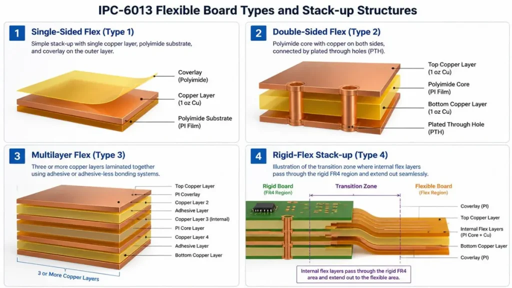
IPC-6013 Flexible Board Types and Stack-up Structures
The baseline architectural builds for high-performance flexible circuitry can be categorized into four primary specifications under IPC-6013 criteria:
- Single-Sided Flex (IPC-6013 Type 1): Consists of a single conductive copper layer bonded to a flexible dielectric base film, protected by a top coverlay sheet. It is best for ultra-thin spaces, static installations, and basic point-to-point connections.
- Double-Sided Flex (IPC-6013 Type 2): Features two conductive copper layers sandwiching a central polyimide core film, with outer layers joined through plated through-holes (PTH) or microvias. It is ideal for high-density routing, component assembly on both sides, and controlled-impedance applications.
- Multilayer Flex (IPC-6013 Type 3): Combines three or more conductive circuit layers bonded together with flexible insulation layers, using complex through-hole and microvia connections. It is best for complex high-speed designs and dense bus architectures.
- Rigid-Flex Stack-Up (IPC-6013 Type 4): Integrates multiple rigid circuit zones directly with flexible layers in a single manufacturing process, allowing multi-layer interconnects to pass seamlessly across flexible boundaries.
Flex PCB Design Guidelines and Engineering Best Practices
Exact Bend Radius Calculations for System Reliability
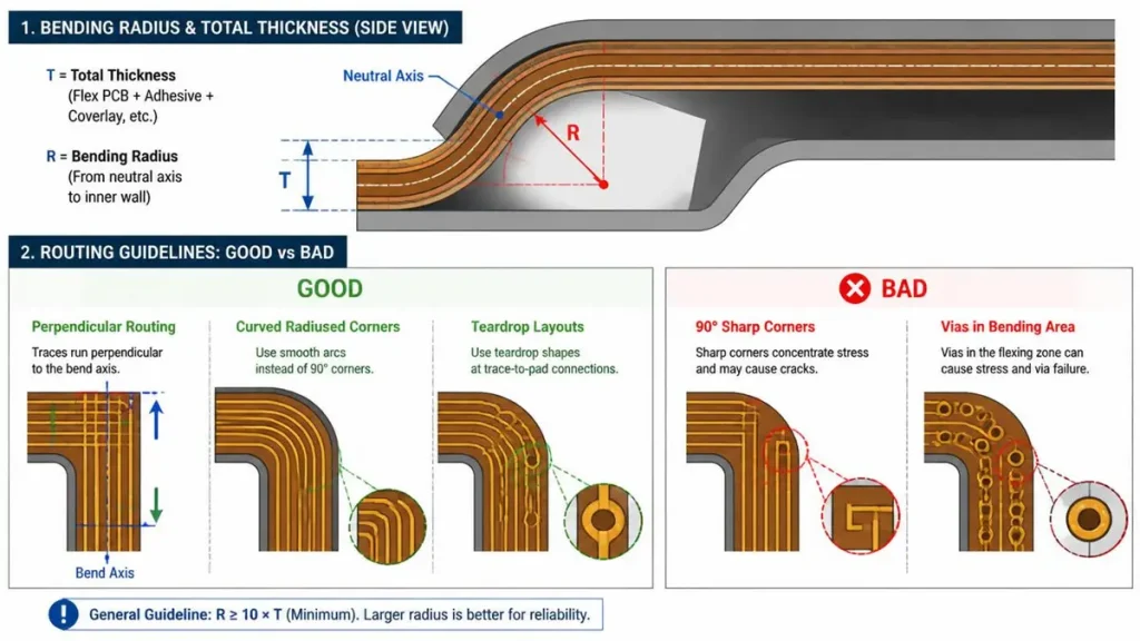
Flex PCB Design Guide: Bending Radius and Routing Guidelines (Good vs Bad)
To prevent copper traces from fracturing, engineers must strictly adhere to maximum and minimum bend radius limits based on the final layer count and operational context:

Where:
= Total thickness of the flexible circuit zone.
= Mechanical application factor:
- = Mechanical application factor:
- K=10 ○ for Single-Sided Static (bend-to-install) applications.
- K=20 ○ for Double-Sided Static configurations.
- K=40 to 100+ ○ for Dynamic, high-cycle flexible applications (requiring specialized single-layer or center-line copper placement to minimize mechanical strain).
Trace Routing and Physical Geometry Best Practices
Traces routed through flexible zones must follow specialized rules to avoid structural failure:
- Perpendicular Routing: Traces should run perpendicular (90∘) to the physical bend axis. Avoid routing lines diagonally or parallel across the bend line to prevent tearing.
- Gradual Transitions: Avoid sharp 90∘ corners or abrupt 45∘ angles. Use smooth, curved radiused corners for all traces in the bend zone to distribute mechanical stress evenly.
- Teardrop Pad Layouts: All component pads, via junctions, and through-holes on a flexible design must feature a teardrop profile. This transition geometry prevents localized stress concentrations where thin lines meet large solid pads.
- Fillets and Anchors: Incorporate mechanical anchor spurs on surface pads to lock the copper down to the substrate and prevent pad lifting during assembly or bending.
Impedance Control and Cross-Hatched Copper Plane Design
Solid copper reference planes provide excellent shielding, but they make thin flexible substrates excessively stiff, which can lead to copper cracking under tight bends. To maintain flexible properties while ensuring controlled impedance for high-speed differential signals, designers use cross-hatched copper planes rather than solid copper sheets.
When implementing cross-hatched grounds:
- Calculate the effective dielectric constant (ϵr,eff), as a cross-hatched geometry lowers the capacitance per unit length.
- Route high-speed differential pairs directly above the solid intersecting paths of the hatch pattern to minimize return-current discontinuities.
Via Placement and Substrate Layer Transitions
- Zero Vias in Bend Zones: Never place a via within or directly adjacent to a designated bend line. Vias introduce rigid, cylindrical structures that act as physical stress concentrators, leading to cracks.
- Staggered Multi-Layer Microvias: When routing multi-layer flexible circuits, stagger vias across adjacent layers rather than stacking them vertically. Stacking vias increases localized stiffness and causes mechanical wrinkling under stress.
High-Density Shielding and High-Frequency EMI Considerations
To control electromagnetic interference (EMI) in high-frequency designs without adding excessive stiffness, use specialized silver conductive ink films or ultra-thin cross-hatched copper shields instead of thick, solid copper planes. These materials provide high RF shielding effectiveness across wide bandwidths while maintaining the substrate’s mechanical flexibility.
Design for Manufacturability (DFM) and Preventing Common Layout Mistakes
- Avoid the “I-Beam” Effect: Never place traces on the top and bottom layers of a double-sided flex board directly over each other. Stacking traces vertically doubles the tension and compression forces on the copper during bending, which can lead to trace failure. Always stagger top and bottom traces relative to one another to distribute the mechanical loads.
- Inner Corner Relief Slots: Internal cutouts, corners, and routing slots must feature clean, rounded radius edges (minimum 1.5mm radius) or be terminated with an intentionally punched circular hole to prevent structural tears from propagating across the polyimide film.
Flex PCB and Rigid-Flex Manufacturing Process (2026 Production Standards)
Overview of Advanced Fabrication Workflows
Manufacturing complex flexible and hybrid rigid-flex circuits requires a precise, multi-step process that combines standard chemical etching with specialized vacuum lamination, laser drilling, and precision alignment systems.
- Material Preparation & Desiccation: Pre-baking polyimide cores to remove structural moisture and stabilize dimensional tolerances.
- Laser Micro-Drilling: Utilizing ultra-short wavelength pulse lasers to define blind or buried microvias without thermal damage.
- Direct Metallization & Desmear: Chemically cleaning the via sidewalls and depositing a conductive structural seed layer.
- Fine-Line Dry Film LDI Patterning & Etching: Projecting circuitry traces through automated imaging systems down to fine micro-line widths.
- Precision Coverlay Registration: Aligning polyimide cover films with exposed surface pads using advanced optical tracking arrays.
- Vacuum Hydropress Lamination: Permanently bonding the multi-layer stack-up together under automated thermal profiles.
- SMT Component Assembly & Reflow: Placing active and passive hardware profiles on stable, rigid-backed array carriers.
- 3D AOI & Flying Probe Electrical Testing: Confirming 100% trace network continuity and identifying any microscopic circuit shorts.
- Reliability Verification: Sampling completed assemblies to check compliance against target bend-cycle endurances.
High-Precision Imaging, Fine-Line Etching, and LDI Systems
To support fine-pitch arrays and advanced packaging footprints, modern 2026 production lines use Laser Direct Imaging (LDI) systems. LDI projects circuit patterns directly onto advanced dry-film photoresists without the alignment errors associated with traditional film negatives. Combined with cleanroom chemical spray etching, this allows for reliable line and space widths down to ≤35 μm, providing high trace density for complex designs.
Vacuum Hydropress Lamination Controls
Laminating flexible polyimide layers, acrylic adhesive sheets, and rigid FR4 sub-panels requires precise thermomechanical control. Automated vacuum hydropresses apply consistent, computerized pressure profiles alongside ramped heating cycles. This controlled environment removes residual air pockets, limits Z-axis adhesive squeeze-out into component windows, and minimizes internal stresses that could otherwise cause board warpage.
Advanced Coverlay Application and Window Profiling
Coverlay openings for surface-mount pads can be created using mechanical punching dies or high-speed UV laser profiling systems. Once the windows are cut, the coverlays are aligned to the etched copper circuits under magnifying optical inspection systems and pre-tacked using a localized heating iron before moving to final vacuum lamination.
Laser Microvia Drilling and Multi-Step Desmear
As via dimensions shrink below 75 μm, standard mechanical drilling becomes unviable due to drill bit deflection and substrate damage. 2026 manufacturing operations rely on hybrid CO2 and UV pulse laser drilling systems to create precise microvias through polyimide and copper layers. Following drilling, boards undergo a specialized chemical plasma desmear process to remove resin debris from the hole walls, ensuring clean, reliable electrical connections across all layers.
Surface Finish Selection for Assembly and Contact Reliability
Selecting the right surface finish depends on the component pitch, shelf life, and whether the board requires dynamic flexing:
- Electroless Nickel Immersion Gold (ENIG): The standard finish for fine-pitch SMT assembly, providing an exceptionally flat planar surface and excellent shelf life. However, the intermediate nickel layer is naturally brittle. For designs subject to severe dynamic bending, ENIG should be restricted to component zones backed by structural stiffeners.
- Organic Solderability Preservatives (OSP): An ultra-thin organic layer that preserves solderability without adding stiff metal intermetallics. This finish keeps the circuit highly flexible and cost-effective.
- Immersion Silver (ImAg) / Immersion Tin (ImSn): Provide flat planar finishes with good conductivity and low signal attenuation at high frequencies, without introducing brittle nickel layers into flexible zones.
Strict Inspection, Automated Testing, and Quality Controls
- 3D Automated Optical Inspection (AOI): Scans completed circuit layers to identify trace geometry variations, micro-shorts, or particulate contamination before lamination.
- Flying Probe Electrical Testing: Validates point-to-point electrical continuity and isolation across complex networks without requiring expensive dedicated test fixtures.
- Reliability and Dynamic Flex Testing: Samples from each production lot are loaded into specialized mechanical cycle fixtures to test continuous bend resistance, ensuring the boards meet performance standards under long-term mechanical stress.
Applications of Flex PCB in Advanced Electronics
High-Performance AI Computing Servers and Flex PCB Accelerator Modules
Modern AI training arrays and high-capacity server systems require dense, high-speed interconnect solutions to manage massive data throughput. Multi-layer rigid-flex backplanes and ultra-thin flexible bridge structures route high-bandwidth communication lines between processing clusters and high-density memory arrays. This setup maintains stable signal integrity at high frequencies while avoiding the space and airflow restrictions of traditional cabling.
Compact AI Cameras and Intelligent Edge Computing Hardware
As advanced vision intelligence and neural processing units are integrated into smaller devices like drones, industrial robots, and compact cameras, internal space becomes highly constrained. Flexible circuits allow image sensor modules to connect directly to central processors around tight internal corners, maximizing space efficiency and ensuring reliable performance in high-vibration environments.
Medical Electronics, Diagnostics, and Wearable Health Technology
In modern medical tech—such as wearable diagnostics, surgical equipment, and implantable biosensors—circuit reliability and biocompatibility are essential safety requirements. Flexible polyimide circuits can conform to ergonomic profiles and withstand regular sterilization cycles, providing reliable electronic connections for high-precision patient care.
Automotive Intelligence: ADAS, EV Battery Systems, and Lighting Modules
The automotive transition toward electric powertrains and autonomous driving systems requires robust, lightweight electronic networks. Flexible circuits are widely utilized in electric vehicle (EV) battery management systems (BMS) to replace complex wiring harnesses with thin, reliable monitoring traces. They are also used to route signals within advanced radar/LiDAR sensors and compact LED headlight assemblies.
High-End Consumer Goods and Foldable Displays
The consumer market relies on flexible electronics to enable innovative form factors, such as foldable smartphones, ultra-thin laptops, and smart consumer devices. These products use high-durability flexible films designed to withstand hundreds of thousands of fold cycles without signal degradation.
Cost Drivers and Pricing Factors in Flex PCB Procurement
Material Cost Analysis: Polyimide vs. Standard FR4
Polyimide base films, specialized acrylic/adhesiveless copper sheets, and protective coverlays cost significantly more than standard glass-epoxy FR4 materials. Understanding how material selection influences production costs is essential for accurate budgeting and project estimation.
| Cost Element | Standard FR4 Substrates | Advanced Polyimide Flex Substrates |
| Raw Material Cost Index | Base Standard (1×) | Higher Premium (3× to 5×) |
| Trace and Via Density Limits | Moderate Paths | High-Density Configurations |
| Z-Axis Thermal Expansion (CTE) | High Expansion | Low, Predictable Expansion |
| Mechanical Profile | Rigid and Non-Yielding | Highly Flexible and Elastic |
Layer Count, Dimensional Scaling, and Panel Utilization
As layer counts increase on flexible or rigid-flex designs, the fabrication workflow requires additional lamination cycles, tighter alignment tolerances, and precise drilling, which increases base production costs. Additionally, because flexible materials are naturally prone to shifting, larger board sizes can reduce panel utilization efficiency, driving up individual unit costs.
Manufacturing Yield Challenges and Complex Mechanical Scrap Rates
Rigid-flex manufacturing involves a multi-step lamination process to combine different materials, which inherently increases production complexity compared to standard rigid boards. Complex outline profiles, deep internal cutouts, and tight window tolerances require specialized laser scoring or precision die cutting, which can increase scrap rates if not optimized during the design phase.
Prototype Sourcing vs. High-Volume Production Run Dynamics
Low-volume prototype manufacturing incurs significant fixed engineering costs, including digital laser programming, material setup, and flying-probe electrical testing. Transitioning to automated, high-volume production lines helps distribute these fixed tooling and processing costs across large runs, significantly reducing the per-unit cost.
Engineering Design Optimization for Cost Reduction
To lower procurement costs without sacrificing performance, consider these design practices:
- Reduce the total layer count in flexible zones by using double-sided or single-sided flex sections where possible, keeping multi-layer routing confined to the rigid zones.
- Use standard, off-the-shelf polyimide and copper film thicknesses to avoid the long lead times and high material costs of custom material specifications.
- Ensure proper spacing between components and flexible bend lines to allow for high-yield, automated SMT assembly and standard reflow soldering profiles.
Comprehensive Comparative Matrix: Flex vs. Rigid vs. Rigid-Flex
To assist engineering and procurement teams in selecting the optimal structural layout for new product development, the following comparative matrix breaks down key performance, cost, and design parameters:
| Operational Parameter | Traditional Rigid PCB | Flexible Printed Circuit (FPC) | Integrated Rigid-Flex PCB |
| Substrate Flexibility | Completely Stiff / Non-Flexible | High Elasticity / Dynamic Bending | Hybrid Zones (Stiff & Flex) |
| Volumetric Efficiency | Low (Constrained to 2D Planes) | Excellent (Folds into 3D Enclosures) | High (Eliminates Connectors) |
| High-Speed Signal Integrity | Moderate (Glass-Weave Skew Risk) | High (Uniform Polyimide Core) | High (Continuous Clean Matching) |
| Mechanical Shock Resistance | Low (Solder Points Can Fracture) | High (Absorbs Vibrations Easily) | High (Protects Critical Zones) |
| Relative Assembly Complexity | Low (Standard SMT Automated Lines) | Medium (Requires Fixtures) | High (Complex Multi-Zone Handling) |
| Initial Fabrication Tooling Cost | Low Base Cost | Moderate Cost Setup | High Tooling Investment Needed |
Reliability, Testing, and Sourcing Compliance Standards
Compliance with IPC Structural Specifications
All flexible and rigid-flex designs must meet strict international manufacturing standards to ensure field reliability:
- IPC-2223: Sectional Design Standard for Flexible Printed Boards. Defines material selection, pad sizes, via placement rules, and bend calculations.
- IPC-6013: Qualification and Performance Specification for Flexible Printed Boards. Governs final quality requirements, testing criteria, and manufacturing tolerances for all classes of flexible electronics.
Mechanical Endurance and Ramped Bend-Cycle Testing
For dynamic flex applications, sample boards from each production run undergo mechanical cycle testing. These tests physically bend the substrate across a fixed radius at a controlled speed for millions of cycles while continuously monitoring trace resistance to detect micro-cracking before failure occurs.
Extended Thermal Shock and Accelerated Environmental Aging
Reliable aerospace, automotive, and industrial components must operate consistently across extreme temperature ranges. Completed boards are subjected to environmental chamber testing—including rapid thermal cycling (e.g., −40∘C to +125∘C), high-humidity storage, and salt spray testing—to ensure long-term resistance to material delamination and copper corrosion.
Documented Failure Modes in Flexible Electronics
Understanding common failure modes helps design teams implement preventative layout choices:
- Trace Fracturing: Occurs when traces are placed too close to a bend axis or designed with sharp 90∘ angles.
- Coverlay Delamination: Often caused by trace contamination, inadequate cleaning before lamination, or improper adhesive flow during pressing.
- Conductor Lifting: Usually results from excessive thermal stress during rework or a lack of proper mechanical anchor spurs on small component pads.
Future Trends in Advanced Flex Technology
Ultra-Thin Substrates and Stretchable Electronics
The demand for smaller, more seamless electronics is driving the development of ultra-thin flexible films and stretchable polyurethanes. These advanced substrates allow circuits to twist, stretch, and conform to irregular, moving surfaces, expanding possibilities for advanced biometric patches and complex industrial sensors.
Structural Integration with Next-Generation AI Hardware Modules
As AI processing power moves to edge devices and dense localized clusters, flexible interconnect architectures are evolving to handle higher component density. Upcoming designs will feature embedded passives, thinner multi-layer stack-ups, and improved thermal materials to handle hot spots in compact, high-power AI modules.
Ultra-High-Speed, Low-Loss Substrates for 5G and Advanced AI Backplanes
Next-generation high-frequency systems require exceptionally clean signal paths. Liquid Crystal Polymer (LCP) and ultra-low-loss adhesiveless polyimide films are becoming critical for high-speed routing. These materials provide low dielectric loss (Df<0.0015), and excellent dimensional stability, ensuring clean, high-bandwidth data transmission at ultra-high frequencies.
How to Choose a High-Capability Flex PCB Manufacturer
Evaluating Technical Fabrication Limits and Capabilities
When sourcing a manufacturing partner for advanced flexible or rigid-flex projects, procurement teams should verify that the supplier can meet the following technical requirements:
- Trace and space width capabilities down to ≤35 μm using high-precision LDI equipment.
- Advanced multi-layer laser drilling equipment capable of drilling microvias down to ≤75 μm.
- Specialization in high-speed, controlled-impedance designs for AI hardware infrastructure.
- Complete in-house testing capabilities, including 3D AOI, flying-probe electrical testing, and automated micro-section analysis.
Verifying Quality Management Certifications
Ensure your manufacturing partner maintains appropriate international quality certifications for your industry:
- ISO 9001:2015: Baseline quality management standard.
- IATF 16949: Required for automotive applications and ADAS systems.
- ISO 13485: Required for high-reliability medical equipment and diagnostics.
- RoHS / REACH Compliance: Ensures environmental safety by restricting hazardous substances.
Conclusion & Strategic Procurement Action Plan
Implementing advanced flexible and rigid-flex PCB technology can improve system density, weight efficiency, and signal integrity in demanding high-frequency designs. However, maximizing these benefits requires close collaboration between design engineers and the fabrication team from the early stages of layout development.
Partnering with Shenzhen Hongda Circuit Technology Co., Ltd. (PCBKR) gives you access to full-service engineering support, precise fabrication, and strict quality control for prototyping and production runs.
Connect with Our Engineering Team
- Request a Technical Project Quote: Send your Gerber files, structural stack-ups, and DFM requirements to our team at sales@pcbkr.com for a complete engineering evaluation.
- Download Our Design Guide Checklist: Access our comprehensive DFM verification guidelines to ensure your flexible layouts are optimized for high manufacturing yields.
- Consult an Engineering Specialist: Work directly with our hardware layout engineers to optimize your material stack-ups and line designs for your performance and cost targets.
Sourcing Manager FAQs: Procuring Flex and Rigid-Flex PCBs
Why are the initial prototype and tooling costs for rigid-flex boards significantly higher than standard rigid designs?
Rigid-flex manufacturing involves a multi-step lamination process to combine different materials, requiring continuous mechanical and laser profiling. The higher initial cost is driven by specialized tooling, individual laser cutting programs, precise layer registration, and dedicated testing fixtures. These upfront costs are distributed across larger production volumes, which significantly reduces the per-unit cost for production runs.
How can our engineering team optimize our flexible layout to lower per-unit manufacturing costs?
To reduce production costs:
Keep flexible layers to a minimum (e.g., using single- or double-sided flex zones where possible), and reserve multi-layer routing for the rigid zones.
Use standard, widely available polyimide core and copper thicknesses to avoid the premium pricing and long lead times of custom materials.
Maintain standard spacing between components and flexible bend zones to maximize production yields and minimize assembly scrap rates.
What are the standard lead times for flexible prototypes compared to large-scale production runs?
Standard quick-turn prototypes for single- or double-sided flexible circuits typically take 3 to 7 working days, while complex multi-layer rigid-flex prototypes require 10 to 15 working days due to the intricate lamination steps. High-volume production runs generally require 3 to 4 weeks, depending on material availability, layer counts, and required quality testing.
Which surface finish is recommended for flexible circuits that undergo continuous mechanical bending?
For flexible sections subject to dynamic, long-term bending, Organic Solderability Preservatives (OSP) or Immersion Silver are recommended. These finishes do not introduce brittle metallic layers. If your design features fine-pitch components that require an Electroless Nickel Immersion Gold (ENIG) finish, ensure those component zones are supported by rigid FR4 or polyimide stiffeners to protect the solder joints from mechanical stress.
What specific quality records and manufacturing documentation should we require for high-reliability projects?
For critical applications, your procurement documentation should require:
Compliance reports verifying adherence to IPC-6013 Class 2 or Class 3 standards.
Micro-section analysis reports to confirm internal copper plating thickness and layer alignment.
Cross-sectional data verifying trace impedance tolerances for high-speed signal paths.
Material certificates confirming compliance with RoHS, REACH, and specified thermal limits.
About Author
David Chen https://www.linkedin.com/in/pcbcoming
David Chen boasts an extensive professional background in PCBA manufacturing, PCBA testing, and PCBA optimization, with specialized expertise in high-precision PCBA fault analysis and rigorous PCBA reliability testing. The author has worked with high-layer-count server PCB fabrication, ultra-low-loss backplane stackups, and thermo-mechanical reliability optimization for AI infrastructure projects involving 112G and 224G PAM4 architectures. Skilled in complex circuit design and cutting-edge advanced PCB manufacturing processes, he delivers solutions that elevate product durability and performance across industrial applications. His technical articles focusing on PCBA manufacturing workflows and testing methodologies are widely cited by industry peers, research institutions, and technical platforms, solidifying his reputation as a recognized technical authority in the global circuit board manufacturing sector.