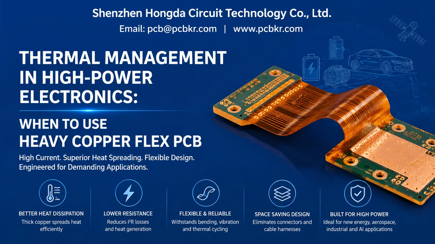
Thermal Management in High-Power Electronics: When to Use Heavy Copper Flex PCB
Power density is climbing faster than most enclosures can dissipate it. Electric drivetrains, aerospace avionics, and edge-AI hardware all share the same design tension: more current, less room, and no tolerance for thermal failure. This is the pressure point where a heavy copper flex PCB stops being a niche option and becomes the practical answer.
At Shenzhen Hongda Circuit Technology Co., Ltd., we build heavy copper flexible circuits for customers who have already tried — and outgrown — standard flex boards. This guide walks through what heavy copper flex PCB technology actually is, why it solves thermal problems that rigid boards cannot, where it fits in 2026-era product design, and what separates a board that survives 100,000 thermal cycles from one that doesn’t.
1. The Thermal-and-Space Conflict Driving Modern PCB Design
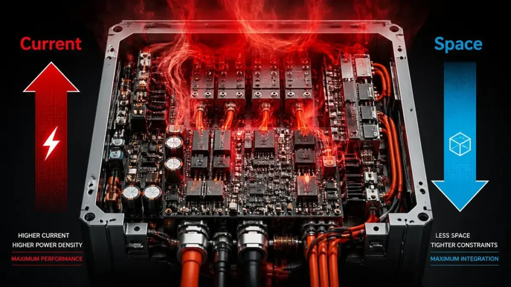
the Thermal-and-Space Conflict Driving Modern PCB Design
Three trends are colliding in high-power product design right now:
- New energy systems (battery packs, inverters, on-board chargers) are pushing toward 800V architectures and higher continuous current ratings, which means more I²R heating in a smaller footprint.
- Aerospace and defense electronics need connections that survive vibration, thermal cycling, and extreme temperature swings without adding weight.
- Compact high-power devices — AI edge accelerators, fast chargers, motor controllers — are shrinking chassis volume while power draw goes up, not down.
A rigid PCB manages copper thickness well but cannot bend into a 3D enclosure. A standard flex PCB bends beautifully but chokes on current above a few amps per trace. Engineers end up choosing between thermal performance and mechanical flexibility — until heavy copper flex circuitry removes that trade-off by combining thick conductive layers with a flexible polyimide base.
2. What Is a Heavy Copper Flex PCB? Core Definitions and Structure
2.1 Heavy Copper Flex PCB Definition and Copper Weight Range
In IPC terminology, “heavy copper” generally starts at 3 oz/ft² (approximately 105 µm) and extends up to 20 oz/ft² or more on specialty builds. A heavy copper flex PCB places that thick copper foil onto a flexible polyimide substrate instead of rigid FR-4, so the circuit can carry high current while still folding, twisting, or dynamically flexing inside the enclosure.
2.2 Heavy Copper Flex PCB vs. Standard Flex PCB
Standard flexible circuits typically use 0.5 oz to 1 oz copper — enough for signal routing and low-current interconnects, but not for power delivery. A heavy copper flexible circuit board changes the copper stack, the etching process, and the lamination pressure profile to accommodate thicker conductors without cracking the flex layer during bend cycling. The result carries significantly more current through the same trace width.
2.3 Heavy Copper Flex PCB vs. Heavy Copper Rigid PCB
Rigid heavy copper boards handle high current well but only in a fixed, planar form factor. A heavy copper flex PCB gives up some of the mechanical rigidity of FR-4 in exchange for routing freedom — the circuit can travel around corners, connect stacked assemblies, or replace a wiring harness entirely. Where a design needs both, that leads to the next structure.
2.4 Rigid-Flex Heavy Copper PCB: Extending the Concept for High-Power Design
A rigid-flex heavy copper PCB combines rigid sections — for component mounting and structural support — with flexible heavy copper zones that carry power between them. This hybrid construction is increasingly common in 2026-era battery management systems and power conversion modules, where designers want the mechanical stability of rigid boards and the space savings of flex circuitry in a single assembly.
3. Thermal Management Advantages: Why Heavy Copper Flex PCB Outperforms
3.1 Higher Copper Thickness Improves Heat Conduction
Copper is roughly 400 times more thermally conductive than the polyimide it sits on. Thicker copper layers act as an internal heat spreader, pulling heat away from hot components before it concentrates at a single junction.
3.2 Lower Conductor Resistance Cuts I²R Losses
Because resistance drops as trace cross-section increases, a heavier copper layer directly reduces I²R heating for a given current load. That means less self-generated heat to manage in the first place — a compounding advantage over thin-copper designs, where resistive losses and thermal stress reinforce each other.
3.3 In-Plane vs. Through-Plane Heat Spreading
Heavy copper flex layers are especially effective at in-plane (lateral) heat spreading — moving heat away from a localized hot spot across the width of the board — which complements through-plane vias and thermal management hardware rather than replacing them. Designers typically combine both paths: heavy copper for lateral spreading, thermal vias or copper coins for vertical extraction to a heatsink.
3.4 Space-Constrained Thermal Performance Through Flexible Routing
Because the circuit can bend, a heavy copper flex PCB often eliminates the connectors and short cable runs that would otherwise sit between rigid boards. Fewer connections mean fewer contact-resistance hot spots and less parasitic heating in an already tight enclosure.
Example in practice: In a new-energy power module, a heavy copper flex PCB can serve simultaneously as the current-carrying conductor and the primary heat-spreading path, reducing or eliminating the need for a separate heat-dissipation structure.
4. Typical Application Scenarios for Heavy Copper Flex PCB
- New energy systems — battery management systems (BMS), DC-DC converters, and power conversion modules where current density and space are both constrained.
- Aerospace electronics — applications demanding high reliability alongside extreme temperature swings, where weight savings from eliminating harnesses also matter.
- Compact high-power devices — AI edge computing hardware and power modules where enclosure volume keeps shrinking even as power draw increases.
- Dynamic or three-dimensional wiring scenarios — high-current designs that need to route around moving parts, stacked PCBs, or non-planar enclosures.
5. Manufacturing Challenges: Where Heavy Copper Flex PCB Gets Difficult
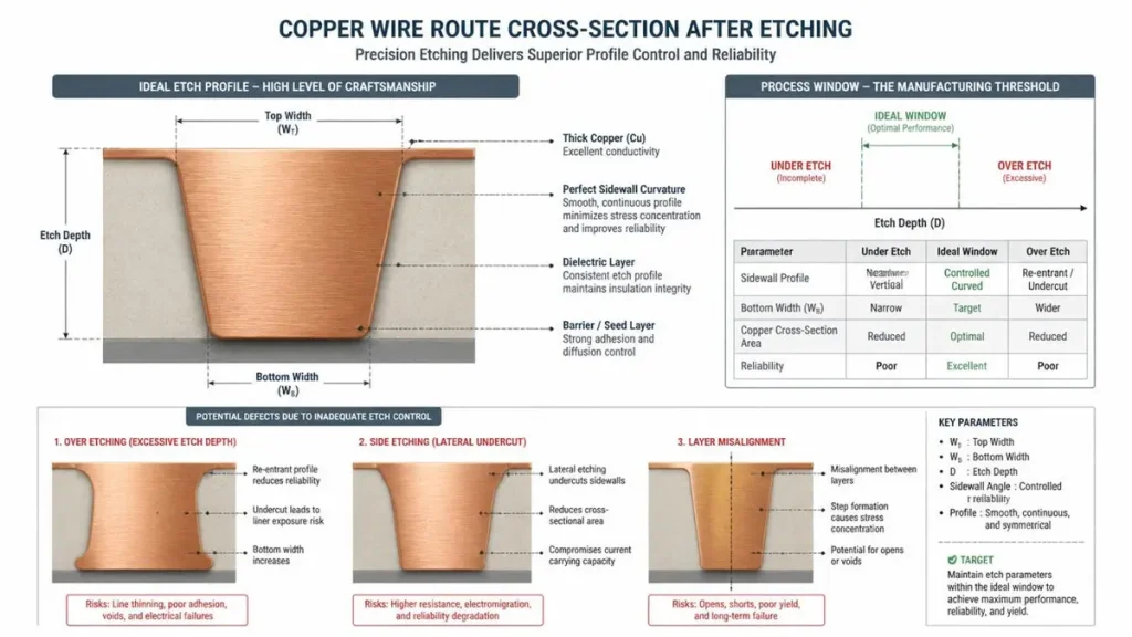
Thick Copper Etch Profile Control and Potential Manufacturing Defects
Heavy copper flex circuits are not simply “thin flex plus more copper.” Several process steps become materially harder:
- Fine-line etching control on thick copper — etching heavy copper without undercutting fine-pitch traces requires tightly controlled etch chemistry and equipment calibration.
- Reliability at the flex-and-heavy-copper interface — thick copper is inherently stiffer, so bend cycling can stress the copper-to-polyimide bond if lamination parameters aren’t matched to the copper weight.
- Lamination and layer-to-layer registration in multilayer heavy copper flex stacks, where uneven pressure distribution can shift alignment across layers.
- Stress and CTE matching in rigid-flex transition zones, where rigid and flexible materials expand at different rates under thermal cycling.
- Drilling, plating, and via reliability — high-current vias need consistent copper plating thickness through a much thicker board stack than standard flex, and drill wander becomes harder to control as copper weight increases.
These are exactly the process variables that separate a supplier who occasionally builds heavy copper flex from one whose core capability is built around it.
6. Rigid-Flex Heavy Copper PCB: Extended Value in High-Power Design
For many high-power product teams, the real design win comes from combining zones within one board:
- Rigid zones carry the component load and give the assembly mechanical support during handling and vibration.
- Flexible zones replace wiring harnesses, save enclosure space, and allow the board to route around obstacles.
- Fewer connectors and cable assemblies mean fewer failure points and lower total system cost over the product’s lifecycle.
- Structural stability under thermal load improves because the rigid sections anchor components while the flex sections absorb mechanical and thermal expansion stress.
7. Manufacturing Capability: What Differentiates a High-End Heavy Copper Flex PCB Supplier
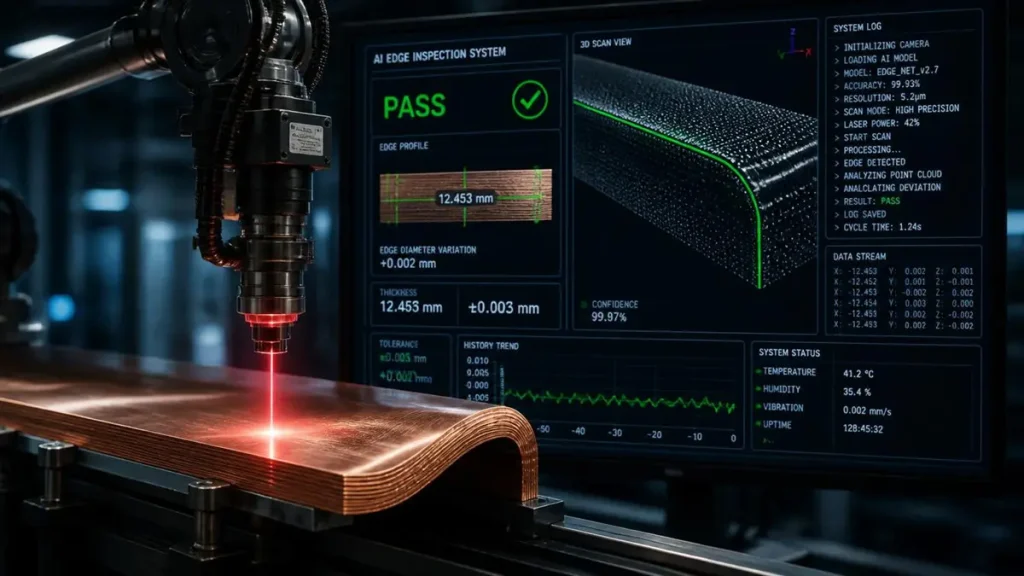
AI-Assisted AOI and Laser Inspection for Heavy Copper Flex PCBs
Not every PCB manufacturer can process heavy copper flex reliably at volume. At Shenzhen Hongda Circuit Technology Co., Ltd., our heavy copper flex PCB manufacturing line is built around a few core capabilities:
- Controlled heavy copper processing — consistent etch and plating control across 3 oz to 20 oz copper weights, holding fine-pitch geometry even at higher copper thickness.
- Multilayer registration and lamination technology — precision alignment across layers, including sequential lamination for rigid-flex hybrid builds.
- Thermal and mechanical reliability testing — thermal cycling, bend-life testing, and high-current burn-in validation before boards ship.
- Process experience specific to high-power applications — engineering support that understands current-carrying capacity, impedance, and thermal design together, not just as separate checklist items.
As PCB manufacturing has moved into 2026, several process advances have become standard on high-end heavy copper flex lines: AI-assisted automated optical inspection (AOI) for catching micro-cracks in thick copper traces, laser direct imaging (LDI) for tighter line-width control at heavier copper weights, and refined sequential lamination profiles that reduce stress at rigid-flex transition zones. These upgrades matter most in exactly the applications this guide covers — new energy power modules and compact high-current electronics — where thermal margin and long-term reliability decide whether a design ships or gets redesigned.
8. Choosing Heavy Copper Flex PCB for Extreme Thermal and Space-Constrained Designs
Heavy copper flex PCB technology exists because thermal density and enclosure space are both moving in the wrong direction for traditional board construction. For designs that need to carry serious current through a shape that a rigid board simply can’t take, heavy copper flex — or its rigid-flex hybrid form — is often the only construction that satisfies both requirements at once.
The deciding factor for high-end applications isn’t just whether a supplier can build heavy copper flex, but whether their process control, testing discipline, and design collaboration hold up across the copper weights, layer counts, and bend requirements a specific application demands.
Frequently Asked Questions
What is a heavy copper flex PCB, and when do I actually need one?
A heavy copper flex PCB uses copper foil at 3 oz/ft² or thicker on a flexible polyimide base, designed for applications that need both high current-carrying capacity and the ability to bend or fold within an enclosure. It’s the right choice when a design has outgrown standard flex copper weights but still needs flexible routing — common in battery management systems, power modules, and compact high-power electronics.
What copper thickness range can heavy copper flex PCB manufacturers typically produce?
Capability varies by supplier, but established heavy copper flex manufacturers generally process copper weights from around 3 oz up to 20 oz/ft², with fine-pitch control becoming more difficult as copper thickness increases. When evaluating a supplier, ask for their proven copper weight range together with the minimum trace width and spacing they can hold at that thickness.
How is a heavy copper flex PCB different from a rigid-flex PCB with heavy copper?
A heavy copper flex PCB is fully flexible throughout. A rigid-flex heavy copper PCB combines rigid sections for component mounting with flexible heavy copper sections for power routing between them. Many high-power designs — particularly BMS and power conversion modules — actually specify rigid-flex construction to get structural support and flexible routing in one assembly.
What should I ask a supplier before sourcing heavy copper flex PCB manufacturing?
Beyond price and lead time, ask about their etch process control for heavy copper, bend-cycle and thermal reliability testing data, multilayer lamination and registration tolerances, and whether they have direct experience with your application category (new energy, aerospace, or compact high-power electronics). Process experience specific to heavy copper — not just standard flex — is the differentiator that shows up in long-term reliability.
Why does heavy copper flex PCB cost more than standard flex or rigid PCB, and is it worth it?
Heavy copper flex circuits cost more due to slower, more controlled etching, specialized lamination profiles, and additional reliability testing required at higher copper weights. For applications where thermal failure or connector-related downtime carries a high cost — power electronics, aerospace systems — the added upfront cost is typically offset by fewer field failures, reduced connector count, and simplified thermal design elsewhere in the enclosure.
Shenzhen Hongda Circuit Technology Co., Ltd. specializes in heavy copper flex PCB and rigid-flex heavy copper PCB manufacturing for new energy, aerospace, and high-power electronics applications. For copper weight capability charts, reliability test data, or a design review for your next high-current flex project, contact our engineering team directly.
About Author
David Chen https://www.linkedin.com/in/pcbcoming
David Chen boasts an extensive professional background in PCBA manufacturing, PCBA testing, and PCBA optimization, with specialized expertise in high-precision PCBA fault analysis and rigorous PCBA reliability testing. The author has worked with high-layer-count server PCB fabrication, ultra-low-loss backplane stackups, and thermo-mechanical reliability optimization for AI infrastructure projects involving 112G and 224G PAM4 architectures. Skilled in complex circuit design and cutting-edge advanced PCB manufacturing processes, he delivers solutions that elevate product durability and performance across industrial applications. His technical articles focusing on PCBA manufacturing workflows and testing methodologies are widely cited by industry peers, research institutions, and technical platforms, solidifying his reputation as a recognized technical authority in the global circuit board manufacturing sector.