Ultimate Guide to Rigid-Flex PCB Manufacturing Process: Advanced 2026 Techniques
The electronics architecture landscape has shifted dramatically. Driven by the explosive growth of AI data infrastructure, high-density edge computing, and complex medical instruments, traditional interconnect methods have met their structural and electrical limits.
Engineers and procurement professionals no longer view the hybrid circuit as a niche luxury. Instead, it has become a fundamental pillar for modern, space-constrained, high-frequency hardware systems.
As an industry-leading partner in advanced printed circuit board fabrication, Shenzhen Hongda Circuit Technology Co., Ltd. delivers this complete, end-to-end technical breakdown of the rigid-flex pcb manufacturing sequence. This guide integrates next-generation process capabilities to assist your engineering and procurement teams in maximizing production yield, ensuring absolute reliability, and optimizing total cost of ownership (TCO).
Overview of Rigid-Flex PCB Fabrication
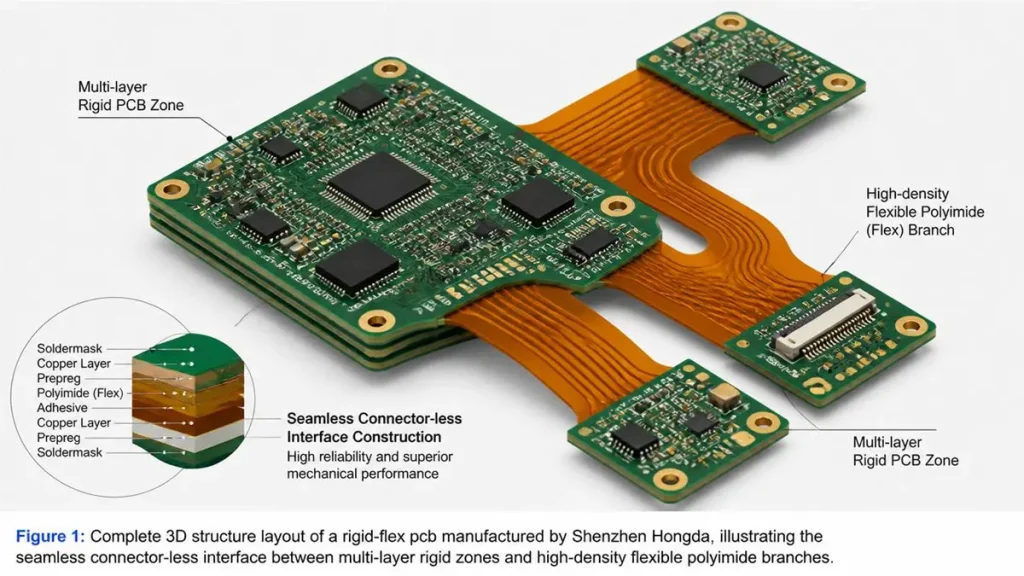
Understanding the modern flex pcb fabrication process requires shifting away from thinking of rigid and flexible components as separate elements joined post-production. Today’s rigid flex pcb process is a unified, highly synchronized co-fabrication workflow.
Rigid-Flex vs. Traditional PCB Manufacturing
Traditional multilayer boards rely entirely on rigid, resin-impregnated glass cloth (such as FR4) as their structural base. Interconnections between separate boards demand heavy board-to-board connectors, wire harnesses, or flat flexible cables (FFCs).
- By eliminating physical connectors and solder joints between sub-assemblies, the architecture removes the most common point of failure under thermal and mechanical stress.
- This hybrid topology reduces the total weight and physical volume of the interconnect system by up to 60%, opening up complex, three-dimensional packaging opportunities.
The Rise of HDI and High-Layer Count Hybrid Stack-Ups
Advanced hardware demands have pushed the envelope far beyond simple 4-layer or 6-layer configurations. High-performance accelerators and modern telecommunication modules regularly deploy high-density interconnect (HDI) structures within the rigid zones of a hybrid board.
By utilizing microvias, stacked or staggered laser-drilled blind and buried vias, and modified semi-additive processes (mSAP), modern fabrication achieves highly compact fine-line trace routing. Multi-layer rigid-flex boards can scale up to 26+ layers, with specialized high-layer count backplanes seamlessly transitioning into multiple high-density independent flexible branches.
Key Manufacturing Steps in Modern Flex and Rigid-Flex Production
Executing a flawless flexible printed circuit assembly requires a multi-stage workflow where environmental variables, material characteristics, and chemical reactions are monitored with extreme precision.
1. Material Preparation and Advanced Substrate Selection
The foundation of a reliable hybrid board relies heavily on its raw material properties. Standard flexible regions utilize copper-clad laminates built from high-Tg Polyimide (PI).
- Adhesiveless vs. Adhesive Laminates: High-reliability applications mandate adhesiveless laminates, where the copper foil is directly cast or electroplated onto the polyimide film. This removes the acrylic or butyral adhesive layers, yielding thinner stack-ups, better thermal stability, and reduced Z-axis thermal expansion risks during lead-free soldering operations.
- RA Copper vs. ED Copper: Selecting the right conductor material is critical. Rolled Annealed (RA) copper features an elongated, horizontal grain structure that delivers excellent elongation properties, making it essential for dynamic applications like hinges or rotating arms. Conversely, Electro-Deposited (ED) copper features a vertical grain structure. While more cost-effective and highly suited for fine-line etching in static applications (where the board bends only once during final housing assembly), ED copper is prone to micro-cracking if subjected to continuous fatigue.
2. Inner Layer Imaging, Graphic Transfer, and Etching
Before any lamination takes place, the inner flexible cores must be thoroughly detailed. The polyimide substrate undergoes a chemical pre-clean followed by the application of a high-resolution dry-film photoresist. Direct Imaging (DI) systems expose the trace patterns directly onto the photoresist without using traditional film artwork, eliminating structural distortion.
The exposed film is developed, and an alkaline chemical etch removes unwanted copper, revealing the delicate circuit geometry. Given the high-speed signaling demands of modern hardware, precise line-width control is strictly enforced to meet exacting impedance specifications.
3. Layer Stack-Up and Sequential Lamination
This stage marks the core structural divergence from standard boards. The etched flexible inner cores are combined with the rigid sections (unclad or copper-clad FR4/no-flow prepreg) using a specialized structural layout.
- No-Flow Prepreg: To prevent resin from flowing into the open flexible zones during press cycles, low-flow or no-flow prepregs are placed between the rigid-flex boundaries.
- Sequential Lamination: The entire stack-up is aligned via high-precision optical pinning systems and placed into a computer-controlled vacuum lamination press. The machine applies a highly specific thermal and pressure profile. This profile balances the varying thermal expansion coefficients (CTE) of the heterogeneous materials, preventing internal mechanical stress or micro-void formation.
4. Precision Drilling, Desmear, and Metal Electroplating
Once fully laminated, mechanical and UV/CO2 laser drilling systems form the microvias and through-holes that connect the rigid outer layers to the flexible inner circuits.
- The Desmear Challenge: Mechanical drilling generates localized frictional heat that melts the polyimide resin, creating an insulating “resin smear” over the inner copper capture pads. A specialized plasma desmear or chemical permanganate process is required to remove this debris, ensuring clean, metal-to-metal contact.
- Plating Through Holes: Following desmear, the entire board undergoes a chemical copper deposition process, followed by electrolytic copper plating. This step establishes uniform, continuous copper walls across all high-aspect-ratio holes and microvias.
5. Outer Layer Processing, Coverlay Application, and Surface Finish
The outer rigid layers are imaged and etched using conventional high-density printing techniques. Concurrently, the exposed flexible sections must be protected against environmental oxidation and short circuits. This is accomplished by applying a Coverlay—a durable layer of polyimide film coated with a thermosetting acrylic adhesive. The coverlay is pre-cut via laser or die punch to expose necessary SMT pads and is then permanently bonded using a localized quick-press lamination cycle.
Finally, the exposed SMT pads receive a high-grade surface finish to ensure optimal solderability and shelf life:
- ENIG (Electroless Nickel Immersion Gold): The premier choice for high-density SMT components, providing an exceptionally flat surface and strong joint integrity.
- OSP (Organic Solderability Preservatives): Deployed selectively depending on mechanical flexibility requirements and the target cost framework.
Critical Process Challenges & Engineering Solutions
Managing Layer Lamination Registration Accuracy
Because polyimide film is naturally flexible, it absorbs moisture and undergoes dimensional shifting during chemical etching and thermal cycling. This dimensional volatility makes multi-layer alignment exceptionally difficult.
Our Solution: At Shenzhen Hongda Circuit Technology Co., Ltd., we use automated optical registration and advanced scaling algorithms. We pre-compensate the material artwork dimensions prior to etching, ensuring that micro-vias hit the center of inner-layer capture pads across every production batch.
Eliminating Failure at the Rigid-to-Flex Transition Zone
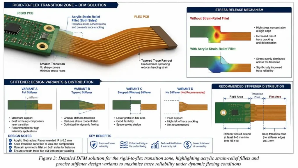
Rigid-to-Flex Transition Zone DFM Solution
The physical interface where the rigid substrate terminates and the flexible polyimide layer extends outward is prone to severe mechanical stress concentrations. Sharp bends or high handling stress at this transition boundary can cause inner trace fractures or copper delamination.
Our Solution: We implement robust Design for Manufacturability (DFM) rules during stack-up configuration. We add specialized flexible adhesive fillets, tapered trace geometries, and localized stiffener design variants (such as FR4, Polyimide, or Aluminum stiffeners) to distribute mechanical strain safely away from critical circuit paths.
Preventing Delamination Risks in Multiple Press Cycles
Complex architectures that require multiple sequential lamination stages expose the internal materials to cumulative thermal stress, which can weaken bonding interfaces over time.
Our Solution: We use advanced vacuum press systems running precise, localized thermal ramp profiles. Combined with high-quality, high-Tg adhesiveless materials, this process maintains strong interlayer peel strength and avoids micro-delamination even under multiple lead-free reflow cycles.
Quality Control & Testing Protocols
Following the completion of structural fabrication, every production lot undergoes a rigorous, sequential testing workflow to guarantee long-term field survivability:
- Automated Optical Inspection (AOI)
- Objective: Scans inner and outer conductor layers before and after lamination.
- Target: Detects localized trace anomalies, micro-shorts, fine-line neckdowns, and spacing violations down to the micron level.
- High-Resolution X-Ray Inspection
- Objective: Provides non-destructive inner-layer analysis.
- Target: Validates internal layer alignment, sequential lamination registration accuracy, and the structural integrity of buried microvia connections.
- Time-Domain Reflectometry (TDR) Impedance Testing
- Objective: Measures precise characteristic impedance across high-speed differential traces.
- Target: Ensures high-frequency signal integrity, verifying that line metrics stay within tight customer-specified tolerances (typically ±10% or ±5%).
- Mechanical Reliability Testing
- Objective: Subjects the board to physical structural strain.
- Target: Differentiates performance based on application type. Dynamic applications undergo continuous automated flexing loops to track bending fatigue life. Meanwhile, static applications undergo controlled radius deformations to confirm assembly resilience.
Manufacturing Capability Checklist
| Process Parameter | Advanced Capability Threshold (2026 Fleet Standard) |
|---|---|
| Maximum Layer Count | Up to 26+ Layers (Hybrid Rigid-Flex Stack-up) |
| Minimum Line Width / Trace Spacing | 2.0 mil / 2.0 mil (50 μm / 50 μm) inside rigid zones |
| Aspect Ratio (Through-Hole Drilling) | 12:1 |
| Microvia Technology | Laser-drilled blind/buried microvias, stacked or staggered |
| Base Materials Available | Dupont Pyralux, Shengyi, Rogers, Panasonic MEGTRON 6/7 |
| Impedance Tolerance Control | ±8% standard (down to ±5% with custom DFM review) |
| Minimum Flex Bend Radius | Up to 10× total material thickness (Static) / 20× (Dynamic) |
| Surface Finishes | ENIG, ENEPIG, OSP, Immersion Silver, Lead-Free HASL |
For complex projects, early collaboration is the best way to prevent manufacturing defects. Our engineering team provides a full Design for Manufacturability (DFM) review before tool fabrication begins. This process optimizes your layer stack-up, refines your impedance models, and ensures smooth transition zone layouts to keep your project on track and within budget.
Need an engineering-validated DFM review or a competitive quote for your next rigid-flex project? Contact our global engineering desk directly at sales@pcbkr.com to connect with a technical specialist.
Procurement Guide: Frequently Asked Questions (FAQ)
What are the key differences between a static flex and a dynamic flex layout, and how do they impact material costs?
A static application is designed to bend or fold only once during final equipment assembly and remain in that fixed position for its entire operating life. This allows for more economical Electro-Deposited (ED) copper configurations and simple stiffener design layouts.
Conversely, a dynamic application undergoes continuous, repeated bending during equipment operation (such as wearable electronics, medical probes, or robotic joints). Dynamic systems require high-grade Rolled Annealed (RA) copper and thinner, symmetrically balanced adhesiveless polyimide laminates. Because RA copper processing involves complex rolling and annealing stages, raw material costs for dynamic configurations are typically 15% to 25% higher than static alternatives.
Why is managing “resin smear” critical during rigid-flex fabrication, and how does your factory handle it?
During mechanical drilling of via holes, the drill bit generates substantial localized friction heat, which exceeds the glass transition temperature (Tg) of the internal polyimide and epoxy resins. This thermal load melts the resin, smearing it across the exposed inner copper contact pads and forming an insulative barrier. If left untreated, this smear will cause intermittent opens or total electrical failure post-plating.
To prevent this, our facility processes all drilled hybrid panels through high-precision plasma desmear chambers, supplemented by localized chemical permanganate etching. This multi-stage process completely removes all resin debris, texturing the internal hole walls to guarantee complete, high-reliability copper plating continuity.
How does your factory maintain tight impedance control profiles across both the rigid and flexible sections of the board?
Maintaining consistent impedance across a hybrid layout is challenging because the dielectric constant (Dk) and material thicknesses change as a trace moves from a rigid FR4 zone into a flexible polyimide zone.
To address this, our engineering team utilizes advanced field solver software during the initial DFM review to calculate tailored, independent trace geometries for each section. In production, we utilize direct laser-guided imaging to maintain trace tolerances within ±10 μm. We then verify performance across every production lot using automated Time-Domain Reflectometry (TDR) testing boards.
What are the main causes of delamination at the rigid-to-flex transition zone, and how do you prevent them?
Delamination at the transition zone is typically caused by moisture trapped within the hygroscopic polyimide film, mismatched thermal expansion coefficients (CTE) among the various substrates, or inadequate resin flow at the boundary. During lead-free reflow soldering (260°C), trapped moisture quickly vaporizes into steam, creating internal micro-voids that tear the material layers apart.
We mitigate this risk by subjecting all flexible inner layers to an extended thermal baking cycle prior to lamination, completely removing residual moisture. Additionally, we use high-performance no-flow prepregs and apply specialized acrylic or polyimide strain-relief fillets along the outer transition borders to distribute physical stress evenly.
What key technical documentation must a sourcing manager provide to get a fast, accurate rigid-flex production quote?
To deliver an accurate, engineering-validated quote, your procurement package should include:
Complete ODB++ data archives or standard Gerber files (including IPC-2581 layout outputs).
An explicit layer stack-up diagram detailing individual material thicknesses, dielectrics, and copper foil weights.
A clear fabrication drawing mapping out the exact dimensions of the rigid zones, flexible sections, and stiffener areas.
Material callouts (such as adhesive vs. adhesiveless cores, RA vs. ED copper, and specific stiffener types).
Desired testing certifications (such as IPC-A-600 Class 2 or Class 3 compliance, UL 94V-0 ratings, or specific RoHS requirements).
Need an engineering-v
About Author
David Chen https://www.linkedin.com/in/pcbcoming
David Chen boasts an extensive professional background in PCBA manufacturing, PCBA testing, and PCBA optimization, with specialized expertise in high-precision PCBA fault analysis and rigorous PCBA reliability testing. The author has worked with high-layer-count server PCB fabrication, ultra-low-loss backplane stackups, and thermo-mechanical reliability optimization for AI infrastructure projects involving 112G and 224G PAM4 architectures. Skilled in complex circuit design and cutting-edge advanced PCB manufacturing processes, he delivers solutions that elevate product durability and performance across industrial applications. His technical articles focusing on PCBA manufacturing workflows and testing methodologies are widely cited by industry peers, research institutions, and technical platforms, solidifying his reputation as a recognized technical authority in the global circuit board manufacturing sector.