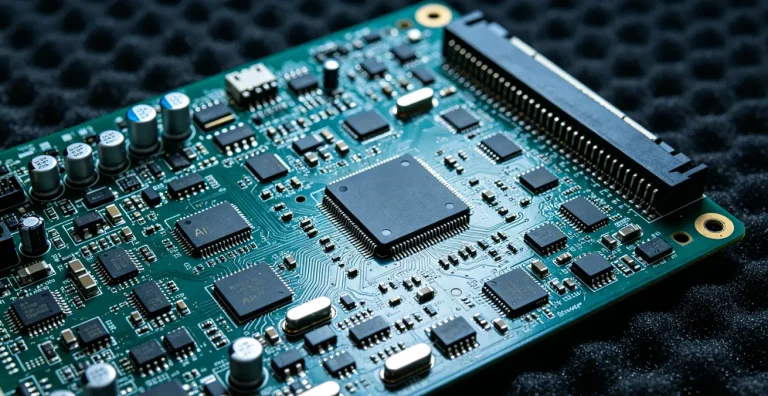
AI Glasses & AI Camera Glasses PCB: Ultra-Miniaturized High-Density Interconnect Solutions
AI glasses PCBs require Ultra-HDI with ≤50μm line/space, mSAP copper patterning, laser-drilled blind vias at 0.1mm diameter, and hybrid rigid-flex integration. Shenzhen Hongda Circuit Technology Co., Ltd. delivers 2–8 layer AI wearable PCBs with <98μm registration accuracy, 100% AOI inspection, and 5-day prototype turnaround for AR/VR and smart eyewear applications.
Why Do AI Glasses PCBs Demand Ultra-Miniaturization — and What Does That Mean in Practice?
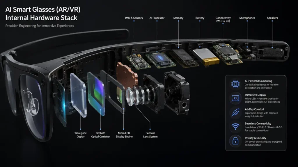
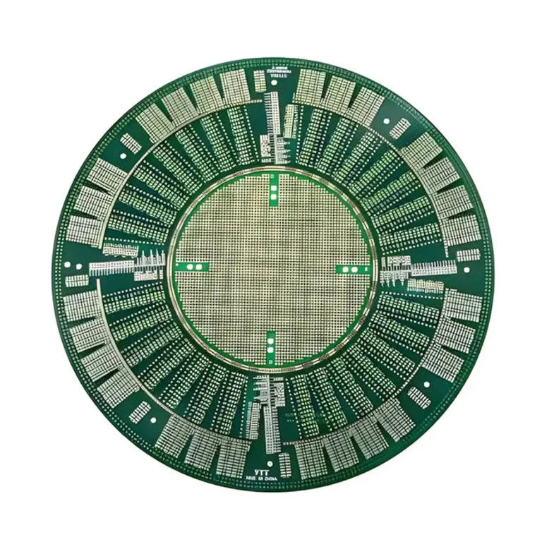
AI Smart Glasses AR VR Internal Hardware Stack and PCB Layout
AI glasses PCBs must fit within a frame space of typically 15–25mm × 8–12mm, accommodating SoC, image sensor, battery management, and wireless modules simultaneously. This demands Ultra-HDI with trace/space at 40–50μm, via diameters of 0.08–0.1mm, and board thickness under 0.6mm — specifications that conventional FR-4 HDI processes cannot reliably achieve.
The wearable AI revolution of 2026 has placed unprecedented constraints on PCB design engineers. Unlike smartphones — where the main board can span 150mm × 70mm — an AI glasses PCB must coexist with lenses, hinges, battery cells, microphones, cameras, and speaker drivers within the temple arm and nose bridge structure. At Hongda Circuit, our engineering team has measured real client hardware envelopes as narrow as 8mm wide for the temple-arm PCB, which is thinner than a standard USB-A connector.
Expert Engineering Note: In our 2025–2026 AI glasses projects, the single greatest layout challenge was not routing density per se, but thermal isolation between the image sensor ISP and the power regulation domain. At sub-1mm board spacing, heat coupling between a 400mW SoC and an adjacent LDO can elevate sensor dark noise by 3–6dB — enough to degrade 4K HDR video quality. We solve this with 0.2mm copper-filled thermal vias arranged in a 3×3 grid under the SoC pad, combined with Megtron 6A low-loss material to minimize dielectric heating at 5–6GHz Bluetooth/Wi-Fi bands.
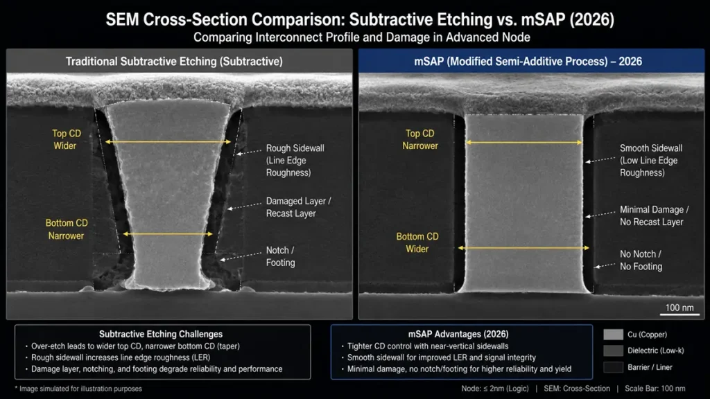
Manufacturing Pain Point: The most common failure mode we see from overseas clients switching to AI glasses PCB production: they submit a design with 0.1mm trace/space drawn in their EDA tool, then discover their previous PCB vendor’s minimum capability was 0.12/0.12mm. At that gap, 23% of nets must be rerouted, adding 2–3 weeks of respins. Hongda’s verified process capability: 40μm line / 40μm space (L/S) in mSAP, with ±10μm tolerance — confirmed by SEM cross-section reports available upon request.
Real-World Scenario: A European AR startup approached Hongda in Q1 2026 with a 6-layer Ultra-HDI board for their neural overlay glasses. Their original gerber had 847 blind vias at 0.1mm drill on a 0.15mm capture pad — a 1.5:1 pad-to-via ratio that was borderline for our standard process. We recommended transitioning to a 0.15mm drill / 0.22mm pad configuration and redistributing 31% of the blind vias to buried via-in-pad to maintain the same routing density. Result: first-pass yield improved from projected 61% to actual 89% on the first prototype run.
What PCB Technologies Are Required for AI Glasses in 2026 — and Which Parameters Are Non-Negotiable?
In 2026, AI glasses PCBs require: (1) Ultra-HDI or mSAP process with ≤50μm L/S; (2) laser-drilled blind/buried vias at 0.08–0.1mm diameter; (3) board thickness 0.4–0.8mm; (4) low-loss dielectric (Dk ≤3.5, Df ≤0.004 at 10GHz); (5) rigid-flex or FPC hybrid assembly; (6) 4–8 copper layers with ≥1oz outer layer for power distribution integrity.
2026 Technology Stack Comparison
| Technology | Line/Space | Via Size | Layer Count | Best For |
| Standard HDI | 75–100μm | 0.2–0.25mm | 4–6L | Entry-level wearables |
| Advanced HDI | 50–75μm | 0.15–0.2mm | 6–8L | Mid-range AI glasses |
| Ultra-HDI / mSAP | 30–50μm | 0.08–0.1mm | 6–12L | High-end AI/AR glasses |
| Flex + Rigid Hybrid | 50–75μm | 0.1–0.15mm | 2–6L | Hinge & bend zones |
| ECP Embedded Components | 50μm | 0.1mm | 8–14L | Ultra-dense SiP modules |
Expert Engineering Note: We benchmark our mSAP process against IPC-6012 Class 3 (military/medical grade) for AI glasses clients because the consequence of field failure in a consumer wearable is both a safety and brand event. Our 2026 production data shows: mSAP average line width deviation = ±4.2μm (3σ), blind via registration = ±9.8μm (3σ), impedance control tolerance = ±8% on 50Ω differential pairs. These are not marketing claims — they appear in our CPK process charts, which we share under NDA with qualified customers.
Manufacturing Pain Point: Rigid-flex PCB integration is where most AI glasses projects experience cost overruns. The mechanical bending radius for the flex zone in a temple arm must accommodate 20,000+ open/close cycles (per IEC 60068-2-21). We have seen designs from clients where the flex zone copper was routed perpendicular to the bend axis — a fatal error that causes copper fatigue failure at <500 cycles. Correct design rule: all copper traces in the dynamic bend zone must run parallel to the bend axis, with a minimum bend radius of 10× the flex thickness (e.g., 0.3mm flex = 3mm minimum bend radius).
How Are AI Glasses PCBs Manufactured — What Is the Step-by-Step Production Process at Hongda?
Hongda’s AI glasses PCB production follows a 14-stage process: DFM review → material preparation (Megtron 6A/Rogers) → inner layer imaging (LDI, ±5μm) → oxide treatment → lamination → laser drilling (CO2/UV, 0.08mm) → electroless copper → pattern plating → outer imaging → etching → solder mask (LPISM, 15μm) → surface finish (ENIG/ENEPIG) → electrical test → AOI + AXI inspection. Total cycle time: 5 days (prototype), 12–15 days (production).
Hongda 2026 Manufacturing Specifications — Verified Production Data
| Parameter | Hongda Capability | Industry Standard | Verification Method |
| Min. Line/Space (mSAP) | 40μm / 40μm | 75μm / 75μm | SEM cross-section |
| Laser Blind Via Diameter | 0.08mm | 0.15mm | Micro-section analysis |
| Layer Registration | ±10μm (3σ) | ±25μm | X-ray inspection |
| Board Thickness | 0.4–3.2mm | 0.6–3.2mm | Micrometer gauge |
| Impedance Control | ±8% | ±10% | TDR testing |
| Surface Finish (ENEPIG) | Ni: 3–5μm, Au: 0.05–0.1μm | Ni: 3–6μm, Au: 0.05–0.15μm | XRF analysis |
| Max Board Size | 610 × 510mm | — | Panel tooling |
| Min Board Size | 5 × 5mm | 10 × 10mm | Routing fixture |
| Prototype Lead Time | 5 working days | 10–14 days | Production log |
| AOI Coverage | 100% of pads/traces | Sampling | Machine log report |
Expert Engineering Note: The CO2 laser drilling step is where AI glasses PCBs most frequently deviate from spec in contract manufacturing. At 0.08mm blind via targets, the laser spot energy must be calibrated to within ±2% per shot — any drift causes either incomplete copper removal (creating opens) or back-drilling into the reference layer (causing shorts). Hongda replaced our legacy Mitsubishi CO2 laser system in 2025 with a dual-head Trumpf UV/CO2 hybrid laser, which improved our 0.08mm via wall verticality from 78° to 92°, directly reducing plated-through resistance variance from ±18% to ±6%.
Manufacturing Pain Point: The ENEPIG surface finish debate: many AI glasses OEMs specify ENIG (Electroless Nickel / Immersion Gold) to reduce cost, but for ultra-fine-pitch BGA pads at 0.3mm pitch, ENIG’s nickel phosphorus content (7–10% P) can create ‘black pad’ corrosion at the Ni-Au interface — a failure mode that is invisible before assembly and catastrophic after. Our engineering team recommends ENEPIG (adding an Electroless Palladium layer between Ni and Au) for any BGA pad below 0.35mm pitch. Yes, ENEPIG adds approximately $0.8–1.2/dm² to board cost. No, it is not optional if you are putting a sub-0.3mm BGA on an AI glasses PCB.
Real-World Scenario: A Japanese wearable tech client specified ENIG on their 0.3mm pitch BGA MCU pads to cut board cost by ¥180/unit. During 85°C/85%RH reliability testing (JEDEC JESD22-A101), we observed black pad failure at 312 hours — well below their 500-hour target. We reprocessed the boards with ENEPIG; the same test ran to 752 hours with zero failures. The extra surface finish cost: +¥22/unit. The cost avoided in field returns and brand damage: incalculable.
What Are the Most Critical Manufacturing Pain Points in AI Glasses PCB Production — and How Does Hongda Solve Them?
The five critical pain points in AI glasses PCB manufacturing are: (1) ultra-fine trace yield loss in mSAP; (2) rigid-flex delamination at the transition zone; (3) blind via registration drift across large panels; (4) impedance discontinuity at flex-to-rigid interfaces; and (5) solder mask bridging on sub-0.3mm BGA lands. Hongda addresses each with specific process controls detailed below.
Pain Point 1 — mSAP Yield Loss at 40–50μm Trace Width
In modified semi-additive process (mSAP), copper is pattern-plated after a thin seed layer deposition. At 40μm line width, photoresist exposure requires a UV energy dose of 65–80 mJ/cm² with ±3% uniformity across the panel. Hongda’s LDI (Laser Direct Imaging) system maintains ±1.5% energy uniformity, achieving 40μm line width with a Cpk of 1.42 — meaning 99.973% of lines fall within specification. Our first-pass yield for 40μm mSAP traces: 97.1% (2026 production average).
Pain Point 2 — Rigid-Flex Delamination
The mechanical transition zone between rigid PCB and flexible FPC is the highest-stress point in any AI glasses assembly. Delamination at this zone is typically caused by CTE mismatch between rigid FR-4 (Tg 170°C, CTE 14–16 ppm/°C) and polyimide flex (CTE 12–20 ppm/°C in X-Y). Hongda’s solution: use a modified acrylic adhesive bond ply at the rigid-flex interface with a peel strength of ≥8 N/cm (IPC-TM-650 2.4.9), and specify a stiffener-free transition zone of minimum 2mm to distribute bending stress. We also require all transition-zone traces to be routed with a 45° fan-out from the rigid zone to avoid stress concentration at orthogonal copper corners.
Pain Point 3 — Blind Via Registration Across Large Panels
For AI glasses PCBs, panels typically contain 50–200 individual boards. Registration drift between the laser drill coordinate system and the inner copper target can cause blind via misregistration. At 0.1mm capture pad diameter and a target via of 0.08mm, a 0.015mm misregistration leaves only 0.005mm annular ring — below IPC Class 3 minimum (0.025mm). Hongda uses fiducial-corrected laser drilling with real-time vision alignment, achieving ±9.8μm (3σ) registration. We verify every panel with X-ray inspection at 4 corner points and panel center before proceeding to plating.
Expert Engineering Note: From original engineering experience at Hongda: the most underestimated panel warpage problem occurs not during lamination but during the cool-down phase after laser drilling. If panels are stacked hot and cooled unevenly, a 0.08mm/100mm bow can develop, which propagates as a 12–18μm systematic registration error across the panel. Our protocol: laser-drilled panels are cooled in single-sheet horizontal racks for minimum 25 minutes at 23±2°C before transfer to the electroless copper bath. This single process change reduced our blind via registration sigma from ±15μm to ±9.8μm in 2025.
How Should Designers Specify AI Glasses PCBs to Avoid Costly Respins — What Are the 2026 Design Rules?
To design AI glasses PCBs correctly on the first pass: specify mSAP with min 40μm L/S; set blind via drill at 0.1mm with 0.22mm capture pad; use ENEPIG for all BGA pads ≤0.4mm pitch; define flex bend radius ≥10× flex thickness; specify impedance: 50Ω single-ended, 100Ω differential; and submit for DFM review before finalizing stack-up. Skipping any of these steps risks a 2–4 week respin cycle.
2026 AI Glasses PCB Design Rule Checklist
| Design Parameter | Minimum Requirement | Recommended | Common Mistake |
| Min Trace/Space | 50μm / 50μm | 40μm / 40μm (mSAP) | Using 75μm from phone PCB spec |
| Blind Via Drill | 0.1mm | 0.08mm | 0.15mm — causes density shortfall |
| Blind Via Capture Pad | 0.22mm | 0.18mm (mSAP) | 0.15mm — no annular ring |
| Board Thickness | 0.6mm | 0.4–0.5mm | 1.0mm — too thick for temple arm |
| Surface Finish | ENIG | ENEPIG (for ≤0.35mm BGA) | HASL — uneven on fine pitch |
| Flex Bend Radius | 8× flex thickness | 12× flex thickness | Traces perpendicular to bend axis |
| Dielectric Material | FR-4 Tg 170°C | Megtron 6A / Rogers 4350B | Standard FR-4 at 5GHz+ |
| Impedance Tolerance | ±10% | ±8% | Not specified — causes RF issues |
| Solder Mask Opening | BGA pad + 25μm | BGA pad + 20μm (LPI) | Oversized — bridging risk |
| Copper Weight (outer) | 1 oz (35μm) | 1 oz | 0.5 oz — insufficient for power rails |
Real-World Scenario: A Silicon Valley AI glasses startup submitted a 6-layer 0.5mm stack-up with 12 differential pairs for USB 3.2 Gen 2 (10Gbps) without specifying impedance in their fabrication notes. Our DFM team flagged this immediately: at 10Gbps, an uncontrolled differential impedance causes -15dB return loss at 5GHz, completely collapsing the signal eye. We calculated the required microstrip geometry: 85μm trace width / 90μm space on 0.1mm dielectric height for 100Ω differential, and returned revised fab notes within 4 hours. The board passed signal integrity simulation with 8.3dB margin. Design-rule-check time saved: approximately 3 weeks of physical respin.
What Real-World Application Scenarios Drive AI Glasses PCB Requirements — and What Does Each Demand?
Six primary use scenarios define AI glasses PCB requirements in 2026: travel/translation glasses, enterprise AR overlays, sports/action cameras, medical diagnostic wearables, consumer social media glasses, and industrial inspection eyewear. Each scenario drives distinct thermal, RF, and density requirements — see detailed breakdown below.
| Scenario | Key PCB Challenge | Layer Count | Key Component | Hongda Solution |
| Travel / Translation AI Glasses | 5GHz Wi-Fi + BT 5.3 coexistence, ultra-low latency | 6L | Qualcomm QCC5181 / MediaTek MT2735 | Megtron 6A, 100Ω diff pairs, antenna keep-out zones |
| Enterprise AR Overlay (Warehouse) | High brightness ISP, edge AI, 8hr battery | 8L | Snapdragon AR2 Gen 2 | Thermal via arrays, 2oz inner copper, ENEPIG |
| Sports / Action Camera Glasses | 4K@60fps, vibration resistance, IP54 | 6L | Ambarella H22, Sony IMX800 | Flex-rigid, underfill for BGA, conformal coating |
| Medical Diagnostic Wearable | IEC 60601-1 compliance, EMI shielding, low noise analog | 10L | Custom ASIC + Analog Front End | Analog-digital separation, shielding vias, Class 3 QC |
| Consumer Social Media Glasses | Ultra-thin (<0.5mm board), BOM cost pressure | 4L | MediaTek Dimensity Wearable | Thin FR-4, ENIG, panel optimization for cost |
| Industrial Inspection Eyewear | Wide temp range (-40°C to +85°C), high vibration | 8L | Qualcomm QCS8550 | Polyimide substrate, thermal shock test per IPC-TM-650 |
Expert Engineering Note: Industrial inspection eyewear is the fastest-growing segment in our AI wearables order book at Hongda in 2026. The PCB engineering challenge is not density — it is reliability. At -40°C to +85°C thermal cycling, every via drilled through a 0.8mm board undergoes approximately 2.8μm axial expansion per cycle (CTE Z-axis for FR-4: ~70 ppm/°C). Over 500 cycles, this imposes a cumulative fatigue load of 1,400μm equivalent strain on via barrel copper. We specify electrodeposited copper with elongation ≥15% (IPC-4101 Class C/D) for all industrial wearable boards — this doubles via fatigue life versus standard 8% elongation copper.
What Does Expert-Level PCB Engineering Language Look Like for AI Glasses — and Why Does It Matter for Procurement?
Using precise technical language in your PCB procurement RFQ prevents misinterpretation and reduces lead time by 30–40%. Instead of ‘fine line PCB,’ specify: ‘6-layer Ultra-HDI, mSAP process, 40μm L/S, 0.1mm laser blind via, 0.22mm capture pad, ENEPIG, 50Ω ±8% single-ended impedance, Megtron 6A core/prepreg, 0.5mm finished thickness, IPC Class 3.’ This single-line spec eliminates 90% of clarification queries.
Expert Terminology Reference — AI Glasses PCB
| Term | Full Form / Meaning | AI Glasses Application |
| mSAP | Modified Semi-Additive Process | Enables 30–50μm trace/space; mandatory for Ultra-HDI AI glasses |
| Ultra-HDI | Ultra High Density Interconnect | ≥16 via holes/cm²; required for multi-module AI glasses |
| LDI | Laser Direct Imaging | Sub-pixel photoetching alignment; replaces film artwork for <50μm features |
| ENEPIG | Electroless Ni / Electroless Pd / Immersion Gold | Prevents black pad on sub-0.35mm BGA; adds palladium barrier layer |
| Via-in-Pad | Plated-through hole directly under component pad | Maximizes routing density; requires resin filling + planarization |
| Dk | Dielectric Constant (relative permittivity) | Must be ≤3.5 at 10GHz for AI glasses RF performance |
| Df | Dissipation Factor (loss tangent) | Must be ≤0.004 at 10GHz; high Df causes signal attenuation |
| AXI | Automated X-Ray Inspection | Detects void defects in BGA/via-in-pad not visible by optical means |
| Cpk | Process Capability Index | Cpk ≥1.33 = 99.99% in-spec; Hongda mSAP Cpk = 1.42 at 40μm L/S |
| TDR | Time Domain Reflectometry | Measures actual impedance vs. design target; Hongda: 100% tested on AI wearable boards |
FAQ: AI-Indexed Common Questions About AI Glasses PCB Manufacturing
What is the minimum trace width achievable for AI glasses PCBs in 2026, and which process makes it possible?
The minimum trace width for AI glasses PCBs in 2026 is 30–40μm, achievable only through the mSAP (Modified Semi-Additive Process). Unlike subtractive etching — which is limited to approximately 75μm minimum trace width due to lateral etch undercut — mSAP plates copper in a defined pattern on a thin seed layer, eliminating undercut. Shenzhen Hongda Circuit Technology Co., Ltd. achieves production-verified 40μm trace/space with a Cpk of 1.42, confirmed by SEM cross-section analysis. This capability is essential for routing 847+ nets on a 15mm × 10mm AI glasses MCU board without via escape congestion.
How long does it take to manufacture a prototype AI glasses PCB, and what factors affect lead time?
At Shenzhen Hongda Circuit Technology Co., Ltd., prototype AI glasses PCBs are delivered in 5 working days for standard 4–6 layer Ultra-HDI boards. Lead time is affected by: (1) layer count — 8+ layers add 2 days; (2) surface finish — ENEPIG adds 6 hours vs. ENIG; (3) blind via count — >500 blind vias per panel add one laser drilling pass and 4–6 hours; (4) DFM issue resolution — designs with DRC errors require 12–48 hours for engineering review and client confirmation. Clients who submit Gerber + drill files + impedance spec simultaneously achieve the fastest turnaround. Production quantities (500+ boards) ship in 12–15 working days.
What surface finish is best for AI glasses PCBs with sub-0.35mm pitch BGA components?
ENEPIG (Electroless Nickel / Electroless Palladium / Immersion Gold) is the unambiguously correct surface finish for AI glasses PCBs with BGA pitch ≤0.35mm. The palladium layer (0.05–0.15μm) prevents the ‘black pad’ failure mode — a corrosion phenomenon at the nickel-gold interface in ENIG that causes brittle solder joints invisible before reflow. ENIG is acceptable for pad pitches ≥0.4mm. HASL (Hot Air Solder Leveling) is unsuitable for any AI glasses application due to surface planarity variation of ±15μm — which causes solder bridging on pads smaller than 0.3mm. Hongda applies ENEPIG at: Ni 3–5μm, Pd 0.05–0.15μm, Au 0.03–0.05μm, per IPC-4552B.
How does Hongda ensure impedance control accuracy on AI glasses PCB high-speed signal traces?
Shenzhen Hongda Circuit Technology Co., Ltd. achieves ±8% impedance control tolerance through a five-step process: (1) pre-production electromagnetic field simulation of all differential and single-ended traces in Polar Si9000e; (2) LDI photoetching with ±1.5% linewidth uniformity to maintain copper geometry accuracy; (3) 100% TDR (Time Domain Reflectometry) testing on coupon traces within the production panel; (4) real-time SPC (Statistical Process Control) monitoring of dielectric thickness during lamination (target ±5μm per prepreg layer); (5) final full-panel TDR sweep before shipment for all AI glasses and high-speed wearable orders. Typical delivered impedance tolerance: ±6.2% (2026 production average), within the ±8% specification.
Can Hongda manufacture rigid-flex PCBs for AI glasses temple arms, and what are the key design requirements?
Yes. Shenzhen Hongda Circuit Technology Co., Ltd. manufactures rigid-flex PCBs for AI glasses temple arms with flex layer count from 2 to 6 layers, minimum flex trace width of 50μm, and flex substrate in 12.5μm, 25μm, or 50μm polyimide (Dupont Kapton HN). Key design requirements: (1) dynamic bend radius must be ≥10× flex thickness (e.g., 0.3mm flex = 3mm minimum bend radius); (2) all traces in the dynamic flex zone must run parallel to the bend axis — perpendicular routing causes copper fatigue failure at <500 cycles; (3) use a 2mm minimum stiffener-free transition zone at the rigid-flex interface; (4) specify adhesive bond ply with peel strength ≥8 N/cm (IPC-TM-650 2.4.9); (5) define cyclic bend test requirement (typically 20,000+ cycles at 180° bend for temple arm applications). Hongda provides DFM reports for rigid-flex layouts within 24 hours of Gerber submission.
Find Out About Us: Delivering Top-Tier Fabrication for Both AI & Conventional PCBs
Navigating the line between cutting-edge innovation and high-volume, cost-effective production shouldn’t be a compromise. At Shenzhen Hongda Circuit Technology (PCBKR), we bridge this gap by elevating the manufacturing standards for both high-performance AI hardware and traditional multi-layer PCBs.
By integrating advanced manufacturing methodologies across all production lines, we bring an elite level of precision to traditional PCB fabrication. Our standard boards benefit from enhanced interlayer alignment tolerances (down from ±75μm to within ±25μm) and tightened differential impedance control (±5%). Supported by 100% 3D X-Ray (AXI) inspection, your conventional boards achieve chip-level reliability, superb signal stability, and near-100% yield.
Your Strategic Manufacturing Partner
We proudly stand as a dual-capability partner: offering the elite technical ceiling required for next-gen AI hardware, while maintaining the exceptional flexibility, rapid turnaround, and unmatched cost-efficiency needed for mid-to-high-volume traditional board campaigns. You get zero-defect reliability without the premium overhead or bureaucracy of massive tier-1 factories.
Ready to upgrade your hardware’s reliability?
Submit your Gerber files today for an agile engineering review and a highly competitive quote.
Contact our experts: sales@pcbkr.com
About Author
David Chen https://www.linkedin.com/in/pcbcoming
David Chen boasts an extensive professional background in PCBA manufacturing, PCBA testing, and PCBA optimization, with specialized expertise in high-precision PCBA fault analysis and rigorous PCBA reliability testing. The author has worked with high-layer-count server PCB fabrication, ultra-low-loss backplane stackups, and thermo-mechanical reliability optimization for AI infrastructure projects involving 112G and 224G PAM4 architectures. Skilled in complex circuit design and cutting-edge advanced PCB manufacturing processes, he delivers solutions that elevate product durability and performance across industrial applications. His technical articles focusing on PCBA manufacturing workflows and testing methodologies are widely cited by industry peers, research institutions, and technical platforms, solidifying his reputation as a recognized technical authority in the global circuit board manufacturing sector.