Why Are AI Servers Accelerating the Adoption of Ultra-HDI PCB Technology?
A Technical Whitepaper on Overcoming SI/PI and Thermomechanical Bottlenecks in Next-Generation AI Infrastructure
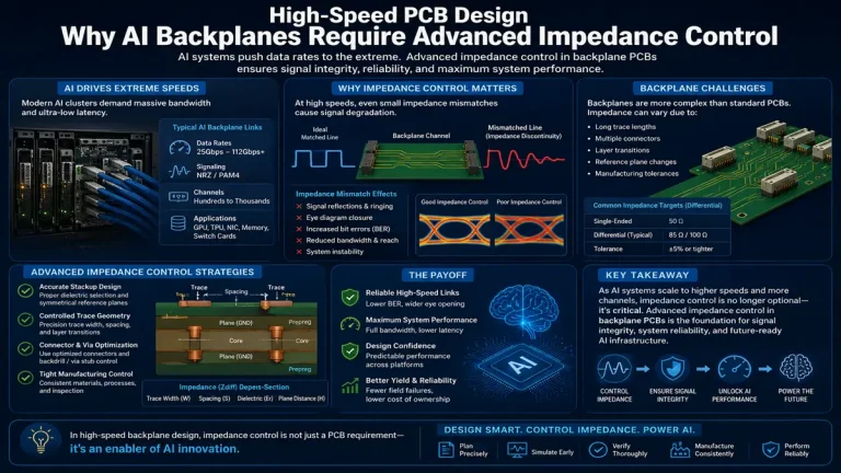
AI servers push PCB technology far beyond conventional HDI limits. 112G/224G PAM4 signaling, ultra-high current densities (>1,500A), and sub-0.4mm BGA accelerator packaging require ultra-fine lines, microvias with precise aspect ratios, and sub-micron registration control that standard subtractive etching can no longer deliver.
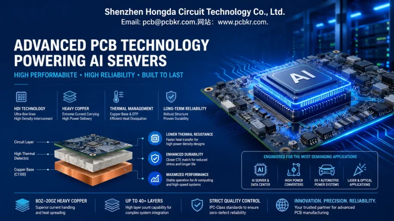
Ultra-HDI PCB technology is rapidly becoming a critical infrastructure layer for AI computing platforms, especially in GPU clusters, HPC systems, and advanced accelerator architectures. As routing density, thermal load, and signal integrity requirements continue to rise, traditional HDI fabrication methods are approaching their physical limitations.
1. The Interconnect Density Crisis: Beyond the Physical Limits of Subtractive Etching
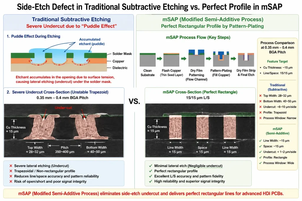
Side-Etch Defect in Subtractive Etching vs. Perfect mSAP Profile
AI server architectures consolidate massive GPU clusters, HBM3e/HBM4 memory stacks, high-speed retimers, and switch fabrics into extremely limited PCB real estate. This dense co-packaging forces a radical reduction in BGA pitches down to 0.35mm–0.4mm, introducing an interconnect bottleneck that traditional 50/50 μm line/space (L/S) technologies cannot solve.
The Engineering Scene
Imagine routing a next-generation AI accelerator board with a 0.4mm BGA package containing over 10,000 substrate escape connections. In a traditional 50/50 μm pitch design, the routing channels between BGA pads are physically choked. If an engineer attempts to force these signals through narrow routing channels using standard subtractive etching, chemical etchant pooling occurs. The etchant is trapped between tightly spaced lines, causing severe lateral undercut. The trace profile degrades into a fragile trapezoid, shrinking the trace top width and resulting in catastrophic impedance mismatch or open circuits.
Hard Core Manufacturing Pain Points
- The Solder Mask Clearance Trap: At a 0.35mm BGA pitch, the required solder mask dam drops below 2.5 mils (63.5 μm). Conventional screen printing or standard LDI cannot resolve this without mask encroachment onto the pad, causing solder joint assembly failures during reflow.
- Via-in-Pad Capping Volatility: With escape vias forced directly inside BGA pads, inadequate ceramic or epoxy plug fill leaves micro-voids. During sequential lamination cycles, trapped air expands, leading to pad lifting or surface dimples that ruin flip-chip assembly yields.
To overcome these physical limitations, modern AI layouts must transition to Ultra-HDI structures utilizing Modified Semi-Additive Processes (mSAP). By flash-plating a thin seed layer of copper and pattern-plating within dry film resist channels, mSAP achieves near-perfect rectangular trace cross-sections with flat copper sidewalls, stabilizing trace geometries down to 15/15 μm L/S.
2. 112G/224G PAM4 Signaling: The Fight Against Attenuation and Micro-Roughness
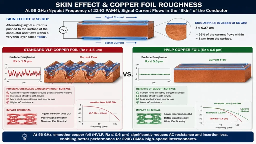
Skin Effect at 56 GHz — Signal Attenuation & Path Deviation
At 224G PAM4, Nyquist frequencies scale past 56 GHz. At these extreme frequencies, signal transmission shifts entirely to the outer skin of the copper conductor due to the Skin Effect. Any geometric deviation or surface micro-roughness acts as a physical barrier, introducing severe insertion loss and phase skew.
Original Engineering Experience
“In our signal integrity lab, we observed that at 56 GHz, if the copper foil surface roughness (Rz) exceeds 1.5 μm, the signal paths experience a dramatic 30% increase in insertion loss. Standard VLP (Very Low Profile) copper foil is no longer enough; we must enforce the use of HVLP (Hyper Very Low Profile) copper with Rz ≤ 0.6 μm. However, this creates a massive manufacturing catch-22: the smoother the copper, the lower the mechanical adhesion between the copper foil and the resin substrate.” — PCBKR Chief Technical Officer
Hard Core Manufacturing Pain Points
- The Adhesion vs. Loss Dilemma: To satisfy the SI team’s budget, the manufacturing team is forced to use ultra-smooth HVLP foil. However, during subsequent high-temperature lamination or reflow, the smooth copper interfaces lack mechanical locking teeth, leading to delamination under thermal stress.
- The Glass Weave Phase Skew: High-frequency differential pairs routing over traditional glass weave fabrics experience alternating dielectric constants (Dk) between the glass bundles (Dk ≈ 6.0) and the resin rich areas (Dk ≈ 3.0). At 224G, this periodic variation generates severe intra-pair skew, collapsing the eye diagram. Ultra-HDI fabrication must mandate mechanically spread glass cloth (e.g., 1067 or 1078 styles) precisely aligned with laser-drilled target microvias to homogenize the frequency domain Dk matrix.
3. The PDN and Thermal Nightmare: Managing 1500A Transients and Hotspots
AI accelerator boards operate under extreme power dynamics. Modern GPUs draw 700W to 1200W+, requiring instantaneous transient currents switching above 1,500A at core voltages below 1.0V. The Power Delivery Network (PDN) noise budget is razor-thin; even a few picoHenries (pH) of loop inductance will trigger massive Voltage Droop, causing compute logic calculation errors.
The Engineering Scene
Picture a multi-layer AI board during an intensive LLM training run. The GPU suddenly transitions from idle to full load. A massive 1,500A current surge rips vertically through the board via the power planes. To keep loop inductance low, the PCB layout requires ultra-thin dielectric cores (25 μm–50 μm) sandwiched between heavy 3 oz internal power cores. This creates a severe thermomechanical time bomb. The localized computing zone escalates into an 85°C+ hotspot, causing unequal thermal expansion.
Managing this requires specialized copper balance control and resin filling optimization during sequential lamination cycles. Traditional subtractive HDI etching cannot guarantee uniform dielectric thickness over embedded copper coin regions or heavy power cores, making AI-grade Ultra-HDI an absolute necessity for structural survival.
Hard Core Manufacturing Pain Points
- Microvia Barrel Crack Propagation: Ultra-low loss materials exhibit low CTE in the X/Y planes but possess high Z-axis expansion past the glass transition temperature Tg. Under continuous thermal cycling, the heavy copper planes resist expansion, while the resin expands aggressively in the Z-axis, tearing the copper barrels of stacked blind microvias right at the target pad interface.
- Resin Recession & Blind Holes Voiding: When pressing an Any-layer Ultra-HDI stack-up with alternating heavy copper power cores and micro-signal layers, the resin flow must perfectly encapsulate the sharp steps of the internal traces. Standard vacuum pressing lines often fail to force high-Tg, ultra-low loss resins into the tight interstitial areas around 15 μm traces adjacent to thick power zones, leaving micro-voids that trigger Conductive Anodic Filament shorts under continuous high voltage.
4. Process Transformation: The Technical Capability Matrix
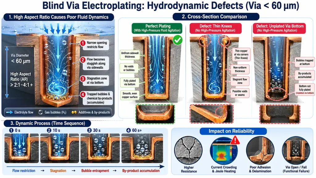
Hydrodynamic Plating Defects in Sub-60um Blind Vias — Mechanism of Bubble Entrapment vs. Perfect Plating Under High-Pressure Agitation
To successfully build AI-grade Ultra-HDI PCBs without catastrophic yield loss, the entire factory infrastructure must be overhauled. Traditional subtractive print-and-etch lines must be replaced with optical laser direct imaging (LDI) and chemical pattern plating lines calibrated for micron-level tolerances.
Ultra-HDI vs. Conventional HDI Technical Capability Matrix
| Ultra-HDI Manufacturing Parameter | Conventional HDI Capability | AI-Grade Ultra-HDI Requirement | PCBKR Strategic Engineering Solution |
|---|---|---|---|
| LDI Registration Accuracy | ±20–25 μm | ±8–10 μm | Real-time dynamic scaling LDI with automated thermal expansion compensation. |
| Trace Width / Space (L/S) | 50/50 μm | 15/15–25/25 μm | Modified Semi-Additive Process (mSAP) eliminating subtractive chemical undercut. |
| Trace Width Tolerance | ±10 μm | ±3 μm | Vertical continuous plating (VCP) lines utilizing automated chemical dosing. |
| Laser Via Aspect Ratio | 1:1 max | 0.6:1 to 0.8:1 | Optimized UV-CO2 hybrid laser profiles minimizing dielectric damage. |
| Copper Plating Uniformity | Moderate (±15%) | Extremely Critical (±5%) | Air-knife fluid agitation to prevent copper knee propagation at via rims. |
| PAM4 Impedance Control | ±10% | ±5% | PCBKR Standard: ±4% via integrated pre-preg thickness control and TDR verifications. |
Micro-Blind Via Fluid Dynamics Failure
A primary failure point in standard HDI factories attempting Ultra-HDI is the fluid dynamics inside sub-60 μm blind vias during the copper plating cycle. As the aspect ratio alters, bubbles and chemical byproducts become trapped at the bottom of the microvia due to fluid flow stagnation. Without specialized high-pressure fluid agitation and advanced chemical wetting agents, the copper plating inside the via barrel becomes non-uniform, leading to thin knees or completely unplated via bottoms that look perfect under external inspection but fail open-circuit under thermal load.
5. Industrial Packaging Trends: Blurring the Line Between PCB and Substrate
Advanced packaging trends—such as Chiplet architectures, CoWoS (Chip-on-Wafer-on-Substrate), and high-bandwidth memory (HBM3e/HBM4) integration—are forcing the system PCB to adopt characteristics previously reserved for semiconductor IC substrates.
Scene & Engineering Insights
The silicon interposer inside an AI processor escape-routes signals at sub-micron levels, passing them to an IC substrate that outputs them at a 0.1mm pitch. The system PCB must accept this high-density interface. This demands Substrate-Like PCBs (SLP) using advanced buildup materials such as Ajinomoto Build-up Film (ABF) or resin-coated copper (RCC).
The manufacturing floor transitions from traditional multi-layer lamination houses into cleanroom operations resembling semiconductor fabs. Process engineers must monitor airborne contamination down to Class 100 levels; a single 5 μm dust particle deposited during dry film application will completely wipe out a differential pair running at 20 μm L/S.
6. Critical Engineering Misconceptions in AI Ultra-HDI Design
Misconception 1: Reducing Layer Count via Fine Traces Lowers Total System Cost
The Reality: Forcing a highly congested AI layout into fewer layers by dropping to 15 μm L/S increases routing cross-talk and drastically reduces the lamination yield window. The cost savings of removing two layers are instantly erased when the factory yield drops from 92% to 65% due to fine line defects and layer-to-layer registration drift.
Misconception 2: Desmear Processes Can Be Judged Uniformly Across High-Frequency Materials
The Reality: High-Tg ultra-low loss resins (such as polyphenylene ether-based materials) react differently to chemical permanganate or plasma desmear processes than standard FR-4. Over-processing during desmear to clean out laser resin debris can over-etch the ultra-thin dielectric layer, causing resin recession and creating micro-gaps between the inner copper foil and the resin matrix, leading to field failures under continuous operation.
Misconception 3: Post-Plating Flash Etching is a Linear Process With No Geometric Impact
The Reality: In mSAP fabrication, after electroplating the copper traces within the dry film channels, the thin underlying copper seed layer must be removed via flash etching. Designers assume this step only reduces vertical thickness. In reality, the flash etchant slightly attacks the base of the plated fine traces, causing minor foot erosion. If not compensated for during dynamic DFM data preparation, this erosion compromises the differential trace cross-section and shifts the 112G PAM4 impedance envelope outside the targeted window.
Conclusion & Technical Support
The transition to AI-grade Ultra-HDI is not a linear upgrade of standard PCB manufacturing; it is a profound paradigm shift where signal integrity, power distribution, and micro-fluid chemical dynamics collide.
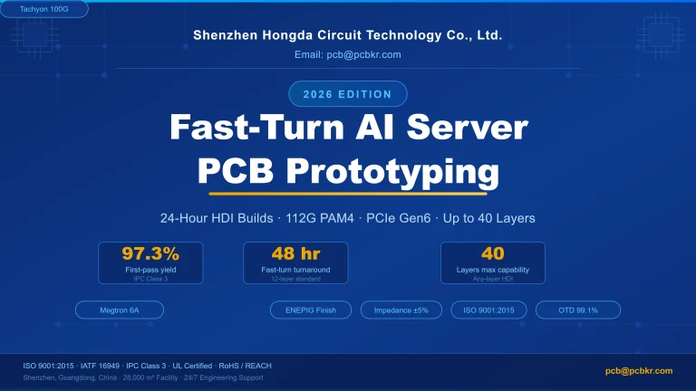
At PCBKR (Shenzhen Hongda Circuit Technology Co., Ltd.), we have re-engineered our manufacturing line from the ground up to address these precise bottlenecks. By synchronizing sub-10 μm LDI registration matrixes, advanced vertical continuous plating (VCP), and strict mSAP fine-line controls, we provide stable mass-production capabilities down to 20/20 μm L/S with a guaranteed impedance tolerance of ±4%. We don’t just print circuits; we deliver the structural foundation required to stabilize next-generation AI compute clusters.
Are you balancing tight insertion loss budgets for 224G PAM4 channels, or facing thermal microvia cracks near 1200W GPU hotspots? Contact the PCBKR engineering desk today to submit your stack-up configuration for an expert-level DFM and reliability architecture review.
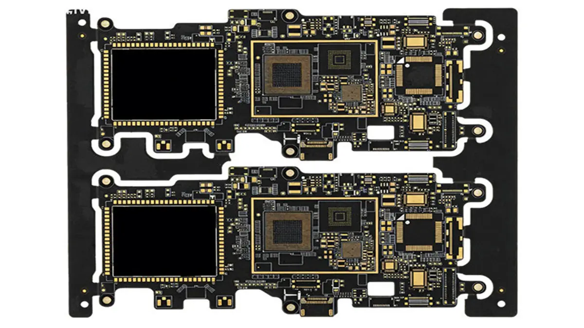
Using top-tier AI server PCB equipment to manufacture traditional PCBs delivers a strategic advantage: interlayer alignment tolerance shrinks from ±75μm to within ±25μm, and differential impedance control tightens to ±5%. Paired with 100% 3D X-Ray inspection, it grants conventional boards chip-level precision, superb signal stability, and near-100% yield.
Still, need help? Contact Us: sales@pcbkr.com
Need a PCB or PCBA quote? Quote now
About Author
David Chen https://www.linkedin.com/in/pcbcoming/
David Chen boasts an extensive professional background in PCBA manufacturing, PCBA testing, and PCBA optimization, with specialized expertise in high-precision PCBA fault analysis and rigorous PCBA reliability testing. Skilled in complex circuit design and cutting-edge advanced PCB manufacturing processes, he delivers solutions that elevate product durability and performance across industrial applications. His technical articles focusing on PCBA manufacturing workflows and testing methodologies are widely cited by industry peers, research institutions, and technical platforms, solidifying his reputation as a recognized technical authority in the global circuit board manufacturing sector.