The Definitive Copper Base PCB Procurement & Supplier TechnicalEvaluation Guide
Copper Base PCB Procurement must prioritize thermal performance reliability, as thermal management has become the primary bottleneck restricting the reliability of high-power electronic equipment, covering automotive traction inverters, EV charging infrastructure, multi-kilowatt AI server power supplies, industrial laser drivers, and high power LED modules. Standard FR4 substrates only deliver a thermal conductivity of around 0.25 W/m·K and act as thermal barriers; relying merely on thermal vias cannot meet the heat dissipation demands of high-current, high-density designs. Copper Base PCBs, a premium category of Insulated Metal Substrates (IMS), adopt solid copper base plates to deliver outstanding heat transfer performance—copper’s thermal conductivity is nearly twice that of aluminum, making such substrates indispensable for next-generation power electronics systems and a core focus of high-quality PCB procurement.
Copper Base PCB Procurement faces prominent supply and manufacturing challenges in the industry. Many general FR4 PCB manufacturers lack dedicated heavy-copper production equipment and mature lamination processes, resulting in frequent critical defects including CTE mismatches between copper and dielectric layers, low precision during heavy copper etching (3 oz to over 10 oz), panel warpage caused by gravity and high temperature baking, dielectric micro-cracking, and post-assembly mechanical fit failures. Low-tier brokers and trading houses further amplify procurement supply risks by substituting high-grade thermal materials and outsourcing production to unqualified small workshops, leading to catastrophic field thermal runaway, board burning, and mass product scrappage, which bring huge economic losses and reliability hazards to end products.
This integrated guide centers on standardized and reliable Copper Base PCB Procurement, combining standardized supplier audit frameworks, deep manufacturing mechanism analysis, and 2026 industry development trends. It provides procurement teams, hardware engineers, and enterprise technical leaders with a complete, actionable set of standards to filter qualified asset-heavy copper base PCB manufacturers and avoid common supply chain pitfalls in the procurement process, so as to guarantee the thermal stability and operational reliability of high-power electronic equipment.
Core Reasons to Choose Specialized Copper Base PCB Manufacturers
1. Unique Thermal Advantages of Copper Base Substrates
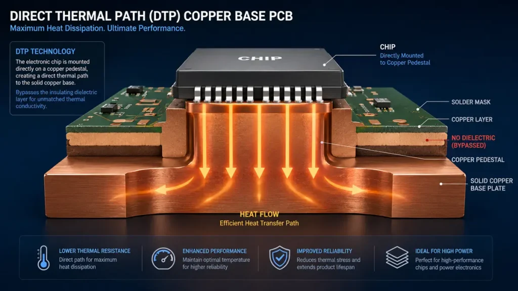
Direct Thermal Path (DTP) Copper Base PCB Structure & Heat Flow Mechanics
Unlike aluminum substrates and FR4 boards, solid copper base plates enable ultra
efficient heat conduction. Advanced dielectric layers with thermal conductivity ranging
from 3.0 W/m·K to 8.0 W/m·K can be matched to copper cores, while Direct Thermal
Path (DTP, also named Copper Pedestal) structures eliminate redundant insulation
layers under high-heat components to build unobstructed heat transfer channels
between chips and base copper plates.
2. Three Unsolvable Pain Points of General FR4 Fabricators
- CTE Mismatch Risk: Copper and dielectric materials feature inconsistent thermal
expansion coefficients. Lamination processes calibrated for lightweight FR4 cannot
suppress delamination and micro-cracks under repeated thermal shock cycles. - Heavy Copper Machining Inaccuracy: Standard drill bits and etching chemicals
fail to maintain stable line width/spacing control for copper weights above 3 oz,
producing irregular traces and dimensional deviations. - Severe Panel Warpage: Solid copper bases carry heavy mass. Ordinary
lamination presses cannot sustain uniform pressure across full panels, leading to
uneven flatness and assembly disqualification.
Ideal Qualified Supplier Profile
A reliable copper base PCB partner must operate dedicated IMS production
workshops with independent heavy-metal processing lines, high-torque CNC milling
equipment, customized chemical etching pipelines, and direct long-term cooperative
relationships with top-tier dielectric material suppliers. Such manufacturers separate
metal substrate production from regular FR4 workflows to eliminate cross
contamination and process parameter interference.
Five Core Technical Evaluation Pillars for Copper
Base PCB Vendors
All supplier qualification audits must cover these five foundational dimensions to fully
verify manufacturing capacity, instead of only checking basic ISO certificates.
Pillar 1: Professional High-Thermal-Conductivity Dielectric Material Management
Qualified suppliers support ultra-thin, high-breakdown dielectric layers with thermal
conductivity of 3.0 W/m·K up to 8.0 W/m·K, including silicon-nitride specialized
formulas. They maintain traceable, stable supply partnerships with world-class
laminate brands: Ventec, Bergquist (Henkel), Laird, Arlon, and Sytech (Shengyi). Every
batch must provide verifiable Material Test Certificates (MTC) to prevent unauthorized
substitution of low-performance 1.0 W/m·K generic fillers for premium high-thermal
dielectrics.
Pillar 2: DTP Copper Pedestal Thermal Separation Design Capability
For devices with extreme heat flux, top-tier manufacturers deliver Direct Thermal Path
(Copper Pedestal) architectures. The dielectric layer is selectively removed to form
integrated raised copper pedestals that directly contact component thermal pads.
Suppliers must guarantee strict micron-level height tolerance between copper
pedestals and surrounding dielectric surfaces and eliminate micro-voids during
lamination to avoid high-voltage dielectric breakdown.
Pillar 3: Precision Heavy Copper Etching & Metal Mechanical Processing
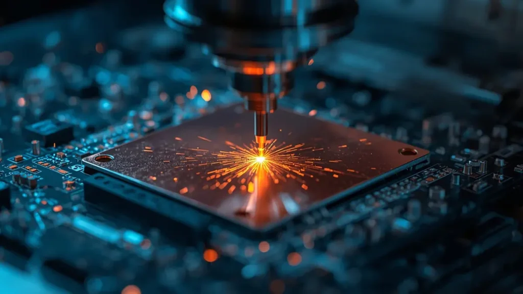
Precision CNC Mechanical Processing for Heavy Copper Base PCB
Processing copper weights from 3 oz to 10 oz and above requires exclusive high
torque CNC routers and heavy-duty punching dies. Factories must deploy customized
etching compensation formulas for thick copper foils to ensure burr-free panel edges;
residual copper burrs on outlines will trigger insulation failure under high working
voltage.
Pillar 4: High-Current Compatible Surface Finish Solutions
Surface finishes must withstand long-duration thermal cycling during soldering.
Qualified facilities maintain stable chemical production lines for three mainstream
processes: ENIG (Electroless Nickel Immersion Gold), LF HASL (Lead-Free Hot Air
Solder Leveling), and OSP (Organic Solderability Preservatives), with complete
process parameter records for mass production traceability.
Pillar 5: Full In-Line High-Power QA Laboratory Testing
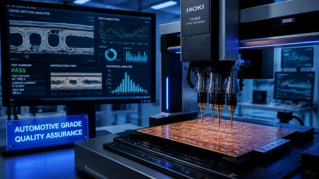
Automated Hi-Pot Inspection & Quality Control for Automotive Copper Base PCBs
Automotive and industrial-grade manufacturers must equip internal dedicated testing
labs to implement 100% inline inspection instead of random sampling, including:
Hi-Pot (High-Potential) isolation testing for all panels
Thermal shock cycling testing to verify thermal cycling resistance
Microsection cross-section analysis to inspect lamination voids
X-ray inspection for blind/buried via filling quality
Peel strength testing of dielectric-copper bonding layers
All test logs, cross-section micrographs, and thermal performance reports must be
delivered together with each shipment for full batch traceability.
Standard Supplier Audit Checklist
| Evaluation Dimension | Core Audit Items | Pass Acceptance Standard |
|---|---|---|
| Technical Performance Parameters | Maximum supported copper weight; dielectric thermal conductivity range; DTP pedestal manufacturing capacity | Copper weight support ≥ 6 oz; dielectric thermal conductivity up to 8.0 W/m·k; stable DTP thermal separation process |
| Production Equipment Layout | Vacuum laminators, thick-copper etching lines, heavy CNC routing machines | Independent metal substrate processing and chemical pipelines; zero cross-production with standard FR4 batches |
| In-House Engineering Capability | DFM (Design for Manufacturability) review and optimization service | Identify unreasonable tolerances, air pocket risks, and asymmetric trace layout defects within 24 hours after receiving Gerber/ODB++ files; provide free complete DFM reports |
| QC Laboratory Infrastructure | Hi-Pot testers, thermal shock chambers, cross-section cutting equipment, X-ray analyzers | Supply full trace documents for each batch: Hi-Pot test logs, thermal shock data, cross-sectional micrographs |
| Supply Chain Resilience | Safety stock of premium thermal laminates; alternative raw material supply channels | Stable warehouse inventory of high-end dielectrics; clear lead-time solutions for unexpected raw material shortages |
Differentiated Factory Selection: Prototyping NPI vs. Mass Volume Production
Copper base PCB projects have distinct demands at different development stages;
matching the right production facility greatly shortens lead time and controls costs.
1. NPI & Prototype Specialized Facilities
1. Zero minimum order quantity (Zero MOQ) to support rapid design iterations
2. Agile front-end engineering teams that actively recommend cost-effective
alternative materials
3. Fast-turn DFM feedback and flexible small-batch lamination parameter adjustment
2. High-Volume Mass Production Facilities
1. Fully automated material handling, AOI automated optical inspection, and closed
loop chemical dosing systems to stabilize CPK process capability values
2. VMI (Vendor Managed Inventory) programs and large-scale stockpiles of heavy
copper raw sheets to mitigate supply fluctuations
3. Mature standardized lamination and baking cycles for 6 oz+ asymmetric copper
boards to control warpage and delamination at scale
Three Major Catastrophic Supply Chain Pitfalls & Risk Warning
Risk 1: Counterfeit Downgraded Dielectric Materials
Unscrupulous brokers replace certified 3.0 W/m·K branded dielectrics with cheap unlabeled 1.0 W/m·K fillers to cut quotation costs. The material difference cannot be detected by appearance inspection and only emerges as thermal runaway and board burnout under long-term operating current. Always require MTC certificates matched to batch numbers before mass production.
Risk 2: “Paper Factory” Middleman Brokers
Many online PCB vendors operate solely as trading intermediaries without self
owned production lines. They outsource complex copper base PCB orders to low
end unknown workshops, resulting in lost production traceability, drifting
machining tolerances, and inconsistent lamination flatness. Avoid partners unable
to provide on-site factory audit access and dedicated metal substrate workshop
photos.
Risk 3: Defective Lamination of Copper Pedestal Structures
Insufficient uniform pressure control during pedestal lamination traps tiny micro
voids between dielectric and copper steps. These voids trigger sudden dielectric
breakdown under high-voltage fields, causing full batch failures during customer
Hi-Pot testing rather than isolated single-board defects. Prioritize manufacturers
with recorded cross-section test data for DTP products.
Ten Technical Interview Questions for Vendor Qualification
Use these standardized technical inquiries to distinguish genuine copper base PCB
manufacturers from resellers during factory audits and quotation communication:
- For designs requiring dielectrics above 3.0 W/m·K, which specific brand series do
you stock? Can you provide verifiable batch-matched Material Test Certificates
(MTC) with each delivery? - What precise etching compensation factor do you apply for heavy copper layers of
3 oz and above? - When fabricating DTP copper pedestal substrates, what maximum mechanical
tolerance do you control for height deviation between copper pedestal tops and
adjacent dielectric layers? - Do you conduct 100% inline Hi-Pot isolation testing in-house? What are your
standard factory test voltage and dwell time for industrial-grade copper base
boards?
- What dedicated equipment and deburring processes do you use during panel
routing to eliminate metallic copper burrs on outer edges? - Is your production facility fully IATF 16949 certified for automotive-grade
manufacturing? Can you share verified reference cases of finished high-power
copper base PCB projects? - If layouts contain laser-drilled blind vias landing directly on solid copper core
bases, do you adopt copper paste plugging or specialized epoxy resin plugging
processes? - What customized lamination press cycles and high-temperature baking routines do
you deploy for 6 oz+ asymmetric copper base layouts to prevent board warpage
and internal delamination? - What is your standard safety stock cycle for high-end thermal laminates such as
Bergquist materials? What is your typical production lead time if primary raw
material supplies face unexpected shortages? - Do you provide a full complimentary DFM manufacturability report with every
engineering review? How many working hours after receiving native Gerber or
ODB++ files will this report be issued?
2026 Key Trends Shaping Copper Base PCB Manufacturing
Three transformative industry shifts must be incorporated into long-term supplier
selection strategies:
- 8.0 W/m·K high-conductivity dielectrics become mainstream automotive
standards: Previously a premium customized option, such materials are now
baseline requirements for EV traction inverters and charging piles, demanding
manufacturers to re-qualify all lamination processes for new generations of high
performance insulation materials. - DTP copper pedestal thermal separation shifts from niche to default design:
High-power LED and industrial laser power supply projects increasingly adopt
direct thermal path structures, raising universal industry standards for micron-level
pedestal height tolerance control. - Full-panel automated inspection replaces sampling QC: Driven by automotive
customer traceability requirements, thermal shock, Hi-Pot, and cross-section
testing are transitioning from periodic batch sampling to 100% per-panel
automated inspection, eliminating statistical quality risks of random sampling.
Technical Consultation & Supplier Cooperation
Navigating high-power electronic thermal design requires a reliable,
experienced copper base PCB manufacturing partner. Shenzhen Hongda
Circuit Technology Co., Ltd. specializes in dedicated metal substrate
production lines separated from standard FR4 workflows, maintains direct
supply channels with top global dielectric brands, and delivers full thermal
shock, peel strength, and Hi-Pot test documentation as standard accessories
for every shipment.
- Upload your Gerber files to request a free, comprehensive DFM
manufacturability review; our cross-disciplinary engineering team will complete
professional assessment and formal quotation within 24 hours. - Direct engineering support email: sales@pcbkr.com
FAQ
What is the main difference between an Aluminum PCB and a Copper Base PCB?
The primary difference lies in thermal conductivity and cost. Copper offers a thermal conductivity of approximately 385 W/m·K, which is nearly double that of aluminum (~205 W/m·K). While Aluminum PCBs are sufficient for standard LED lighting, Copper Base PCBs are mandatory for high-power electronics (like EV traction inverters or multi-kW AI server power supplies) where junction temperatures are extreme and heat must be dissipated rapidly to prevent device failure.
How can I verify if a Copper Base PCB supplier is using premium or counterfeit dielectric materials?
Counterfeit or downgraded dielectric material is the most common sourcing trap; unbranded 1.0 W/m·K fillers look identical to premium 3.0 W/m·K+ laminates on data sheets. To prevent this, you should always demand a batch-matched Material Test Certificate (MTC) from established high-Tc brands like Ventec, Bergquist, Laird, Arlon, or Sytech before volume production. Genuine fabricators with direct supply chain tracing will provide these logs transparently with every shipment.
What is Direct Thermal Path (DTP) in Copper MCPCBs, and when do I need it?
Direct Thermal Path (also known as a Copper Pedestal PCB) is an architecture where the insulating dielectric layer is selectively removed under high-heat components. This allows the component’s thermal pad to come into direct, mechanical contact with the solid copper base. You need DTP when your design deals with extreme heat flux (e.g., high-power industrial lasers or next-gen EV charging infrastructure) where even a high-conductivity dielectric layer creates an unacceptable thermal barrier.
Why do standard FR4 board houses often fail when manufacturing Heavy Copper/Copper Base PCBs?
Standard PCB shops lack the dedicated heavy-metal lamination presses and specialized chemical etching lines required for thick copper handling (3 oz to over 10 oz). This lack of specialization leads to three catastrophic defects: CTE mismatch (causing internal delamination or micro-cracking under thermal cycles), trace width inaccuracy due to poor thick-copper etch compensation, and severe panel warpage caused by the immense weight of the solid copper base during high-temperature baking.
What QC testing should be standard for automotive or industrial-grade Copper Base PCBs?
Beyond basic ISO or IATF 16949 certificates, a qualified manufacturer must perform 100% inline inspection rather than random batch sampling. Standard trace documentation delivered with your boards should always include Hi-Pot (High-Potential) isolation test logs to check voltage withstand, Thermal Shock testing data to ensure delamination resistance, and Microsection cross-sectional micrographs to verify the absence of micro-voids trapped within the lamination layers.
About Author
David Chen https://www.linkedin.com/in/pcbcoming
David Chen boasts an extensive professional background in PCBA manufacturing, PCBA testing, and PCBA optimization, with specialized expertise in high-precision PCBA fault analysis and rigorous PCBA reliability testing. The author has worked with high-layer-count server PCB fabrication, ultra-low-loss backplane stackups, and thermo-mechanical reliability optimization for AI infrastructure projects involving 112G and 224G PAM4 architectures. Skilled in complex circuit design and cutting-edge advanced PCB manufacturing processes, he delivers solutions that elevate product durability and performance across industrial applications. His technical articles focusing on PCBA manufacturing workflows and testing methodologies are widely cited by industry peers, research institutions, and technical platforms, solidifying his reputation as a recognized technical authority in the global circuit board manufacturing sector.