Copper Base PCB Manufacturer Guide 2026: Specifications,Applications, and Buyer’s Selection Criteria
Copper Base PCB is the standard fix for a problem that FR-4 laminate cannot solve: getting
heat out of a circuit fast enough to keep a high-power design alive. Thermal failure remains
the leading cause of premature breakdown in high-power electronics, and it is rarely the
semiconductor that fails first — it is the board underneath it. For engineers and
procurement teams sourcing boards for LED arrays, power modules, EV components, or
industrial drives, copper base PCB construction has become the default answer.
This guide breaks down what a copper base PCB actually is, how it differs from aluminum
base and heavy copper boards, where 2026 manufacturing advances have changed what’s
possible, and what to check before choosing a supplier — starting with the process
capability a qualified manufacturer should be able to show you upfront.
What Is a Copper Base PCB? Understanding Copper Based PCB Construction
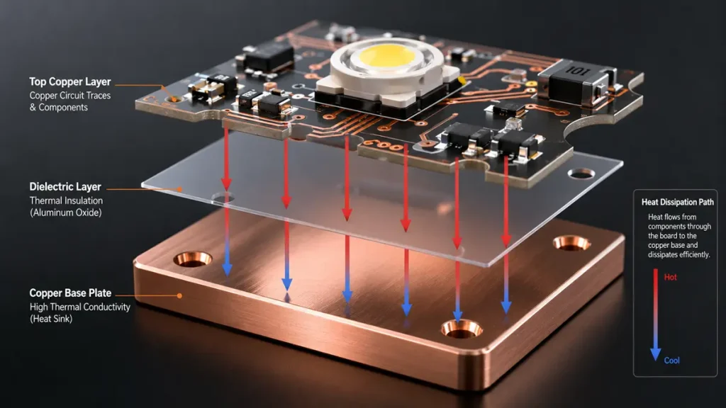
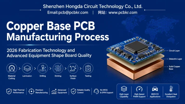
Copper Based PCB Cross-Section: Vertical Heat Dissipation Path
A copper base PCB — sometimes written as copper based PCB — uses a solid copper plate
as its structural core instead of a fiberglass (FR-4) substrate. A thin, thermally conductive
dielectric layer sits between the copper base and the copper circuit layer, electrically
isolating the circuitry while still allowing heat to pass through to the base almost as
efficiently as through solid metal.
The core difference from standard FR-4 boards is thermal path, not electrical performance.
FR-4 is an effective insulator and a poor heat conductor, so heat generated by a component
has nowhere to go but sideways through the copper traces. A copper base PCB instead
gives that heat a short, vertical path straight down into a solid metal plate, which then
spreads it across a much larger surface area — typically into a heatsink or chassis.
This construction is why copper base boards show up wherever components run hot: LED
drivers, motor controllers, power converters, and high-current switching circuits.
Copper Base PCB Structure: From Copper Base to Copper Circuit Layer
A copper base PCB is built from four functional layers, and understanding each one matters
for both design and sourcing decisions:
1. Copper base plate — the structural and thermal foundation, typically 1.0–3.0 mm
thick, providing mechanical rigidity and heat spreading.
2. Dielectric layer — a thin, thermally conductive insulating layer (often a ceramic-filled
polymer) that separates the circuit from the base while allowing heat transfer.
3. Copper circuit layer — the patterned conductive layer where traces, pads, and
components sit, available in a range of copper weights.
4.Surface finish — protective and solderable coating such as ENIG, HASL, or OSP,
applied over exposed copper.
Some designs add thermal management features on top of this base structure — embedded
copper coins, thermal vias, or cavity designs — to move heat away from especially dense hot
spots even faster.
Key Advantages of Copper Base PCB and Copper Based PCB Technology for Buyers
The technical properties of a copper base PCB only matter if they translate into something
a buyer can act on. Here is what each advantage means in practical terms:
1. High thermal conductivity — copper conducts heat roughly twice as well as
aluminum, which means a copper base PCB moves heat away from components
faster, allowing higher power density in the same footprint.
2. Better heat spreading uniformity — a solid copper plate distributes heat more evenly
than a segmented or laminated structure, which reduces localized hot spots that
shorten component life.
3. Support for high-power devices — components rated for higher current or wattage
can run within their thermal limits instead of derating, which protects both
performance and warranty margins.
3. Improved long-term reliability — lower operating temperatures translate directly
into slower degradation of solder joints, dielectric material, and semiconductor
junctions, which for a buyer means fewer field failures and warranty claims.
4. Reduced thermal cycling stress — copper’s mechanical stability under repeated
heating and cooling reduces the risk of delamination over the product’s service life,
which matters most for automotive and outdoor applications with wide temperature
swings.
Copper Base PCB vs Aluminum Base PCB: Choosing the Right Metal Core Substrate
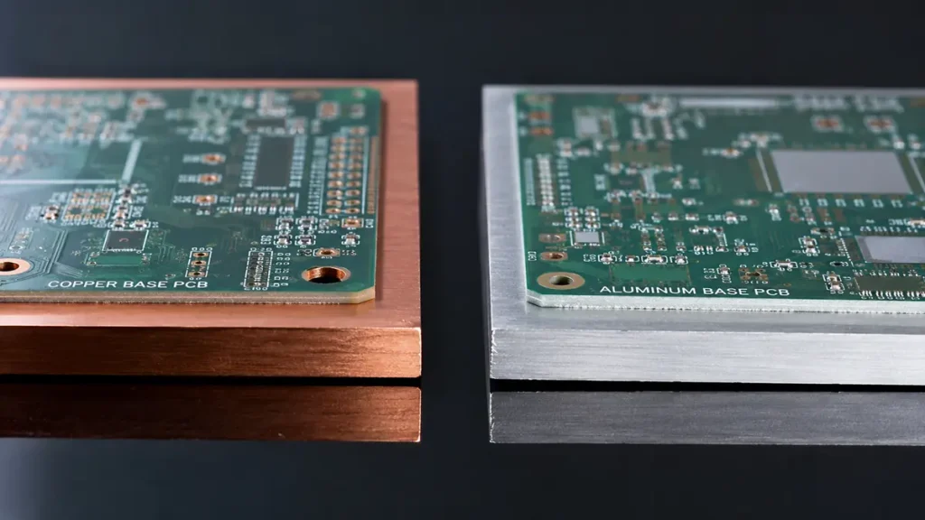
Material Comparison: Copper Base PCB vs Aluminum Base PCB Side-by-Side
Copper base and aluminum base PCBs are often grouped together as “metal core PCBs,” but
they are not interchangeable, and the choice affects both performance and cost.
| Factor | Copper Base PCB | Aluminum Base PCB |
|---|---|---|
| Thermal conductivity | Higher (better heat dissipation) | Lower, but adequate for moderate loads |
| Mechanical strength | Higher, more rigid | Lighter, more workable |
| Weight | Heavier | Significantly lighter |
| Cost | Higher material and processing cost | More cost-effective for standard applications |
| Best use cases | High-power modules, automotive, industrial drives | General LED lighting, consumer electronics |
| Design considerations | Requires attention to weight and mounting | Easier to machine and shape |
Aluminum Base PCB 3oz Copper vs Standard Copper Base Boards
A common point of confusion is comparing an aluminum base PCB built with 3oz copper
circuitry against a true copper base board. The “3oz copper” here refers only to the
thickness of the circuit layer sitting on top of the aluminum core — the base material is still
aluminum, not copper. A board like this can carry more current than a standard 1oz
aluminum board, but it will not match the heat-spreading performance of a solid copper
base structure. Buyers comparing quotes should confirm whether “copper” in the spec
sheet refers to the circuit layer or the base plate — the two get conflated more often than
manufacturers would like to admit.
Copper Base PCB vs Heavy Copper PCB: Clearing Up a Common Confusion
These two terms get used interchangeably in RFQs, but they describe two different design
decisions.
1. Copper base PCB is a question of substrate structure — what material forms the
board’s core.
2. Heavy copper PCB is a question of circuit layer thickness — how much copper sits in
the conductive traces, regardless of what the base is made of.
A board can be a heavy copper PCB built on standard FR-4, on aluminum, or on a copper
base — the terms describe different layers of the same board and are not mutually
exclusive.
Heavy Copper PCB Base Material Explained
“Heavy copper” generally refers to circuit layers at 3oz (105µm) copper weight or above,
used when a design needs to carry high current directly through the traces rather than
through external busbars. When heavy copper circuitry is combined with a copper base —
rather than FR-4 — the result is a board optimized for both high current carrying capacity
and aggressive heat dissipation, which is why the two specifications are frequently ordered
together for high-power converters and welding equipment.
Common Applications of Copper Base PCB in 2026
1. LED lighting — high-power LED arrays and street lighting fixtures where junction
temperature directly determines lumen output and lifespan.
2. Power electronics — DC-DC converters, inverters, and switching power supplies
where component density keeps increasing.
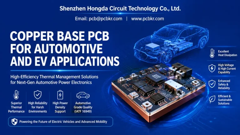
3. Automotive and EV systems — onboard chargers, battery management systems, and
motor drive modules operating in wide temperature ranges.
4. Industrial control equipment — motor drives, servo controllers, and welding power
sources subject to sustained high current.
5. High-current modules — busbar-integrated boards and power distribution
assemblies.
6. Thermal management assemblies — boards designed specifically to double as a heat
spreader for adjacent components.
2026 Copper Base PCB Manufacturing Technology: What’s New
Copper base PCB fabrication has moved well past the “thicker copper, thinner dielectric”
approach that defined the category for years. Several manufacturing shifts are now shaping
how these boards are specified and built.
2oz Copper Base Metal PCB Production Advances
Precision etching and plating control have made 2oz copper circuit layers on metal base
boards far more consistent than they were even a few years ago, narrowing trace tolerance
and reducing impedance variation across a panel. This matters directly for buyers: tighter
process control means less variation between production lots, which reduces the
qualification burden when moving from prototype to volume manufacturing.
Ultra-Thick Copper and Ultra-Thin Dielectric Innovations
The demand from EV and AI-server power supplies has pushed manufacturers toward
heavier copper base plates (up to and beyond 3mm) paired with thinner, higher
performance dielectric layers than were previously viable. The net effect is a board that
dissipates heat faster without adding proportional thickness or weight — a direct response
to power density requirements that have climbed steadily as switching frequencies
increase and component packages shrink.
Laser Drilling and Via Precision
Laser-drilled microvias have become standard on higher-spec copper base designs,
replacing mechanical drilling in areas requiring tight via placement near thermal pads. This
allows denser component placement without compromising the thermal path beneath
high-power devices.
Automated Optical and Thermal Inspection
Manufacturing lines increasingly pair automated optical inspection (AOI) with thermal
imaging validation on copper base boards, catching dielectric voids or delamination risk
before boards leave the factory — a meaningful reliability improvement for buyers who
cannot afford field failures in automotive or industrial deployments.
Design and Manufacturing Considerations for Copper Base PCB
Before finalizing a design, work through these variables with your manufacturer:
1. Copper thickness selection — both base plate and circuit layer thickness affect
current capacity and thermal performance; over-specifying adds unnecessary cost.
2. Thermal performance requirements — define the actual junction-to-ambient target
rather than defaulting to the thickest available copper.
3. Drill and plating considerations — via placement near thermal pads needs
coordination between the electrical and thermal design.
4. Layer structure constraints — single-layer copper base boards are the most common
and cost-effective; double-sided and multilayer options exist but add complexity.
5. Surface finish options — ENIG is standard for fine-pitch components; HASL remains
a lower-cost option for simpler assemblies.
6. DFM review points — copper base boards are less forgiving of design errors than FR 4 because rework after fabrication is far more limited.
7. Prototype vs mass production issues — tooling and panelization decisions made at
prototype stage should already account for volume production requirements to avoid
a second design cycle.
How to Choose the Right Copper Base PCB Manufacturer
Selection criteria for buyers should go beyond price per board:
1. Power load and heat dissipation requirement — match the manufacturer’s
demonstrated thermal performance data to your actual application, not just a generic
datasheet.
2. Environmental operating temperature — confirm the supplier has experience with
your target temperature range, especially for automotive or outdoor use.
3. Mechanical stress tolerance — vibration and shock requirements should be validated
against the manufacturer’s test data, not assumed.
4.Budget and total cost of ownership — the lowest quoted price is rarely the lowest
cost once failure rates and requalification are factored in.
5.Lead time and production capacity — ask specifically about capacity for your order
volume, not just prototype turnaround.
6.Supplier capability and certifications — verify ISO 9001 (and IATF 16949 for
automotive work) along with actual copper base PCB production experience, not just
general PCB capability.
Copper Base PCB Quality and Testing Standards
A credible copper base PCB manufacturer should be able to demonstrate, not just claim, the
following:
1. Thermal resistance testing — measured junction-to-case or junction-to-ambient
data, not estimated figures.
2. Electrical reliability checks — continuity, insulation resistance, and dielectric
withstand testing on every production batch.
3.Dimensional inspection — automated optical inspection against design tolerances.
4.Solderability testing — verification that surface finish performs reliably through the
customer’s assembly process.
5.Surface finish quality control — consistent plating thickness and coverage across the
panel.
6.Reliability validation — thermal cycling and, where relevant, vibration testing
aligned to the end application’s operating environment.
Copper Base PCB Pricing Factors
Copper base PCB pricing varies more than standard FR-4 pricing because several material
and process variables compound:
1. Board size and panel utilization
2. Copper base thickness
3. Circuit layer copper weight
4. Dielectric material selection
5. Layer count
6. Surface finish type
7. Order quantity
8. Lead time requirements
9. Custom or non-standard specifications
Because these variables interact, an accurate quote requires a complete specification —
board size, copper weights, dielectric type, and finish — rather than a single “price per
square inch” estimate.
Frequently Asked Questions About Copper Base PCB
What is the difference between copper base PCB and aluminum base PCB?
The core difference is the base material and resulting thermal performance. Copper conducts heat more efficiently than aluminum but is heavier and costs more, making it the better fit for high-power applications where aluminum base boards would run too hot.
Is copper base PCB suitable for high power applications?
Yes. Copper base PCB is specifically used in high-power applications — power converters, motor drives, and high current LED arrays — because its thermal path handles sustained heat loads that would cause standard FR-4 or aluminum boards to derate or fail prematurely.
What copper thickness is best for my project?
It depends on current-carrying requirements and thermal load. Lower current, general-purpose designs can use standard 1oz circuit copper on a copper base, while high-current designs typically require 2oz to heavy copper (3oz+) circuitry combined with a thicker base plate.
Can copper base PCB support prototype orders?
Yes, most manufacturers with in-house copper base capability can produce small prototype runs, though minimum order quantities and lead times are typically longer than for standard FR-4 prototypes due to material and tooling requirements.
What is the typical lead time?
Prototype lead times for copper base PCB commonly run longer than standard boards because of material sourcing and specialized processing; production lead time depends on order volume, copper thickness, and current factory capacity — confirm current lead times directly with your manufacturer rather than relying on generic industry estimates.
Shenzhen Hongda Circuit Technology: Copper Base PCB Process Capability
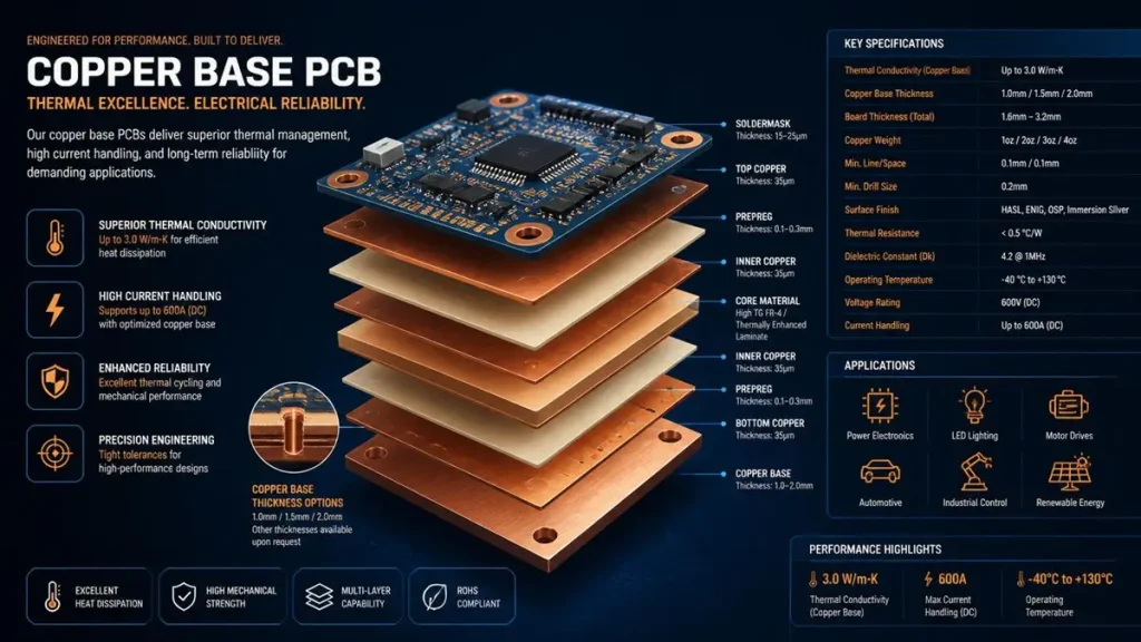
Shenzhen Hongda Copper Base PCB 3D Exploded View & Engineering Specifications
| Parameter | Capability |
|---|---|
| Base material | Copper base (C1100 / C1020 pure copper), aluminum base, heavy copper base |
| Copper base thickness | 0.8 mm – 3.0 mm |
| Circuit layer copper weight | 1oz – 6oz (heavy copper up to 10oz on request) |
| Dielectric layer | Thermally conductive polymer / ceramic-filled, 0.075 mm – 0.15 mm |
| Thermal conductivity (dielectric) | 1.0 – 3.0 W/m·K |
| Layer count | Single-sided, double-sided; multilayer copper base on request |
| Board thickness | 0.6 mm – 3.5 mm (finished) |
| Min. trace / space | 4 mil / 4 mil |
| Min. hole size | 0.2 mm (mechanical), laser microvia on request |
| Max. panel size | 500 mm × 600 mm |
| Surface finish | ENIG, HASL (lead-free), OSP, immersion silver |
| Solder mask | White, black, green (thermally stabilized for high-temp operation) |
| Testing capability | AOI, flying probe / E-test, thermal resistance testing, dimensional inspection |
| Certifications | ISO 9001; UL-recognized materials on request |
| Prototype lead time | 3–5 working days |
| Mass production lead time | 10–15 working days (volume and spec dependent) |
This capability range covers the majority of LED lighting, power electronics, automotive,
and industrial control designs discussed below. For specifications outside this range,
request a feasibility review before finalizing a design.
Get Your Copper Base PCB Quote from Shenzhen Hongda Circuit Technology
Shenzhen Hongda Circuit Technology Co., Ltd. produces copper base PCB, heavy copper
PCB, and aluminum base PCB for customers across LED lighting, power electronics,
automotive, and industrial control applications. To move a project forward:
1.Request a Quote — submit board size, copper weight, and layer count for a same
cycle quotation.
2. Send Gerber Files — upload design files directly for a DFM review before tooling
begins.
3.Ask for a DFM Review — get engineering feedback on copper thickness, via
placement, and thermal path before committing to production.
4.Discuss Thermal Requirements — talk through your application’s power load and
operating environment with an engineer before finalizing specifications.
About Author
David Chen https://www.linkedin.com/in/pcbcoming
David Chen boasts an extensive professional background in PCBA manufacturing, PCBA testing, and PCBA optimization, with specialized expertise in high-precision PCBA fault analysis and rigorous PCBA reliability testing. The author has worked with high-layer-count server PCB fabrication, ultra-low-loss backplane stackups, and thermo-mechanical reliability optimization for AI infrastructure projects involving 112G and 224G PAM4 architectures. Skilled in complex circuit design and cutting-edge advanced PCB manufacturing processes, he delivers solutions that elevate product durability and performance across industrial applications. His technical articles focusing on PCBA manufacturing workflows and testing methodologies are widely cited by industry peers, research institutions, and technical platforms, solidifying his reputation as a recognized technical authority in the global circuit board manufacturing sector.