Copper Base PCB Design and Manufacturing: An Engineering Guide to Working with a Copper Base PCB Manufacturer
Copper Base PCB Manufacturer provides copper base PCB technology that has evolved from a niche thermal management solution into a mainstream core component widely adopted in LED lighting, automotive power modules, motor drives, and industrial power supply equipment.
For hardware engineers, the core confusion rarely lies in “why choose copper substrates”, but how to lock key design parameters before PCB layout, and what critical technical questions to communicate with such manufacturers before mass production.
Shenzhen Hongda Circuit Technology Co., Ltd. works with design teams at exactly this stage, translating copper thickness, board thickness, hole structure, and clearance requirements into a manufacturable stack-up before the first Gerber file is even generated. This guide walks through the design rules, DFM checkpoints, and manufacturing capabilities that separate a smooth copper base PCB production run from a costly redesign.
What a Copper Base PCB Manufacturer Needs to Know Before Design Starts
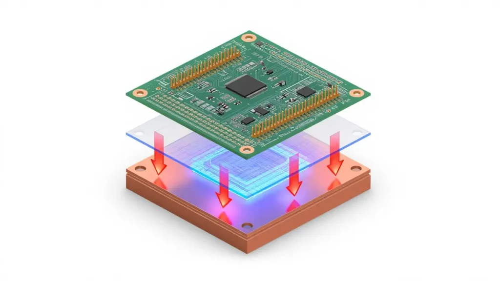
Exploded 3D view of a high-performance copper base PCB showing its thermal-management stack-up layout.
A copper core PCB — sometimes called a copper substrate PCB or copper metal core PCB — replaces the fiberglass core of a conventional board with a solid copper base, giving it thermal conductivity that a standard FR-4 board cannot approach. Before any layout work begins, three sets of information should be confirmed with your fabrication partner.
Application Requirements: Current, Voltage, and Thermal Path
Design decisions on a copper base PCB start with the operating environment rather than the stack-up itself. Engineers should define the working current density and acceptable temperature rise, the intended heat-dissipation path (natural convection, forced air, or liquid cooling), the voltage class and associated insulation requirements such as creepage distance and dielectric withstand rating, and the mounting method together with mechanical constraints like board thickness, mounting hole placement, and enclosure clearance.
Confirming Manufacturing Capability with Your Fabrication Partner
Every copper base PCB manufacturer has a different process window, and it is far cheaper to learn those limits before layout than after DFM review. Items worth confirming up front include maximum and minimum board thickness, maximum panel size, and the achievable copper thickness range; minimum trace width and spacing, minimum hole diameter, and minimum finished plated-hole diameter; whether the factory supports heavy copper or copper-composite structures, and whether it has dedicated thermal-management processes such as thermal via arrays or heavy copper etch capability.
Material Selection and Compliance Standards
The base material — FR-4, high-Tg laminate, aluminum-composite, or copper-composite — should be selected alongside RoHS and REACH compliance requirements. Where the application calls for it, the design should also reference recognized standards such as IPC-2221, IPC-2222, and IPC-A-600 so that acceptance criteria are unambiguous on both sides of the order.
Copper Base PCB Design Rules: Copper Thickness, Trace Width, and Spacing
Once the application requirements are set, the detailed copper base PCB design rules govern how the board actually gets built.
Copper Thickness Selection for Heavy Copper PCB Applications
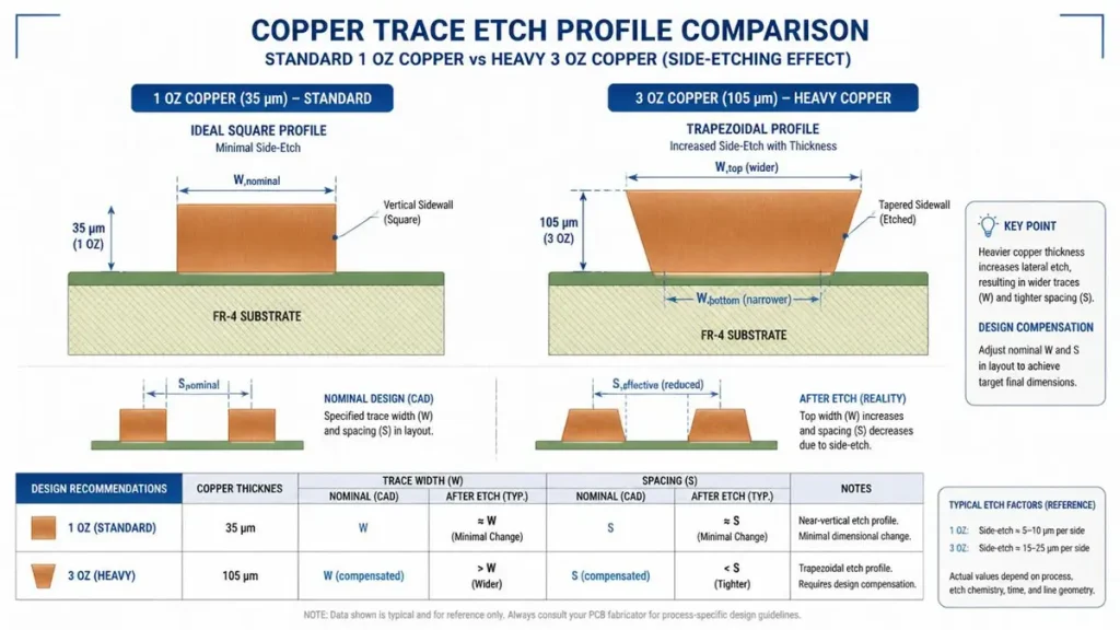
Technical diagram comparing PCB copper trace etching profiles between standard 1 oz and heavy 3 oz copper with side-etching effect.
Finished copper thickness — including plating — should be selected by current density rather than by habit. Ordinary signal traces typically start at 1 oz / 35 µm and increase according to permissible temperature rise. High-current traces and power planes commonly move into the 2–3 oz range, with local reinforcement where needed, while heavy copper PCB designs at 3 oz and above require particular attention to etch capability and the resulting trace width and spacing limits. Copper thickness and trace geometry are not independent variables: thicker copper produces more pronounced side-etch, so width and spacing must scale up with copper weight, and for high-current traces it is usually more effective to increase trace width in combination with copper thickness than to rely on copper thickness alone.
Board Thickness and Hole-to-Thickness Ratio
Standard board thickness options of 1.0 mm, 1.2 mm, and 1.6 mm should be adjusted for structural strength and heat-dissipation needs. Copper-base and heavy-copper boards need enough overall stiffness to avoid warping or thermal-stress concentration, and deep or large-diameter holes require a controlled thickness-to-hole-diameter ratio to prevent drill breakage or poor hole-wall quality.
Trace, Clearance, and Spacing Design Rules
Line-to-line, line-to-hole, and hole-to-hole spacing should be set from the factory’s etching and drilling capability, with an added DFM margin, and high-voltage areas need extra electrical clearance in line with IPC guidance on creepage distance. Component-to-component and component-to-board-edge spacing also needs attention: surface-mount spacing is typically kept above 20 mil, ICs above 80 mil, and BGAs above 200 mil, and tall components — anything above roughly 10 mm — should keep a 5 mm keep-out zone free of low-profile parts. On the trace side itself, minimum width and spacing should be calculated from current and temperature rise, then rounded up to the manufacturer’s process capability; high-current traces benefit from short, wide runs, parallel segments, and supporting thermal vias, while high-speed signals need controlled impedance, length matching, a continuous reference plane, and the familiar 3W spacing rule with accompanying ground vias. Power traces, in turn, should favor planes or wide copper pours to minimize loop area and improve return-path performance.
Thermal Pads and Heat-Dissipation Via Arrays
Power pad or thermal pad dimensions should follow the component datasheet and match the assembly line’s placement accuracy, and thick-copper or high-current pads need to account for remaining copper after etch as well as solder mask clearance. Thermal via arrays placed under heat-sensitive components or power pads improve conduction, and via diameter, pitch, and fill method must match the manufacturer’s process to avoid voiding or incomplete solder fill.
Common DFM Risks in Copper Base PCB Fabrication
Several recurring issues account for most yield problems on copper base and heavy copper boards, and each one is preventable at the design stage.
- Insufficient trace width or spacing. Designs that exceed a factory’s etching capability lead to open circuits, shorts, or uncontrolled impedance; heavy copper boards are especially prone to side-etch and need extra spacing margin.
- Hole and hole-wall problems. Holes that are too small, or a thickness-to-diameter ratio that is too aggressive, cause drill breakage or rough hole walls, and insufficient copper fill in plated holes creates long-term reliability risk.
- Pad and component mismatch. Pad size and spacing that do not match the component footprint lead to poor solder joints or bridging, and high-density packages such as BGA and QFN are especially sensitive to DFM deviations, making strict adherence to the footprint library essential.
- Process-edge conflicts. Components or cutouts placed too close to the process edge, tooling strip, or ICT fixture holes can cause fabrication or test failures, and missing tooling, ICT, or fiber-alignment holes complicate assembly and testing later.
- Thermal and structural conflicts. Tall components positioned over a heat sink’s projected footprint can block the cooling path, and inadequate spacing between heat-generating and heat-sensitive parts leads to localized overheating.
Copper Base PCB DFM: From Prototype to Mass Production
Design intent shifts meaningfully between a prototype run and a mass-production release, and copper base PCB DFM should shift with it.
Prototype-stage priorities center on validating function and key performance quickly, which often means allowing some process margin and a less-than-optimal layout, and using standard materials with relaxed DFM constraints while keeping electrical performance as the priority. Mass-production priorities are broader: DFM and DFR need to be addressed comprehensively so the design is repeatable, cost-effective, and consistent at volume, and trace width and spacing, hole structure, pad sizing, and panelization all need to match the factory’s process capability precisely. In short, prototypes are optimized to run; production designs are optimized to run, to build cleanly, and to be serviceable, with DFM tightened across the board and margin reserved for testing, rework, and burn-in.
Advanced PCB Manufacturing Technology and Equipment at Shenzhen Hongda Circuit Technology
Copper base and heavy copper PCB fabrication places real demands on process equipment, and Shenzhen Hongda Circuit Technology Co., Ltd. has built its production lines specifically around those demands.
Precision etching and thick-copper processing
Etching heavy copper without losing trace definition requires tightly controlled etch-compensation and line-width control systems, which our production floor applies consistently from 1 oz signal layers up through heavy copper power layers.
Laser direct imaging (LDI) and thermoelectric separation
LDI exposure removes the registration drift associated with conventional phototooling, giving tighter, more repeatable trace geometry on copper core boards, while our thermoelectric separation process isolates the circuit layer from the copper base electrically while keeping the thermal path direct — the structure that lets heat move straight from a component into the copper substrate.
Controlled drilling and via fill
CNC and laser drilling systems are matched to copper base board thickness-to-hole ratios, supporting the small-diameter, high-density via arrays that heat-sensitive components and power pads require, with via-fill processes tuned to avoid voiding.
Automated optical inspection, X-ray, and impedance verification
Every panel passes through AOI for pattern verification, X-ray inspection for buried and blind via integrity, and impedance testing for controlled-impedance nets, so that copper thickness, trace geometry, and hole quality are confirmed against the released design before the board ships.
Engineering-led DFM review
Rather than a one-way file check, incoming designs go through a structured DFM pass — stack-up and copper-thickness review, trace and spacing verification, hole and pad-stack checks, and a dedicated thermal/structural review for heavy copper or high-density boards — so issues are caught during layout review, not after the first article.
File Checklist for Copper Base PCB Manufacturing Orders
A smooth production start depends on submitting a complete file package rather than iterating after the fact. A typical submission to a copper base PCB manufacturer includes the following.
- Design files: native PCB source files with a version note, a complete BOM listing part numbers, packages, quantities, and key parameters, and a schematic PDF with net labels and interface notes.
- Manufacturing and process files: Gerber files covering circuit layers, copper layers, solder mask, solder paste, drill, and silkscreen; a drill drawing or drill table with hole type, diameter, and tolerance; and a process note specifying copper thickness, board thickness, surface finish, impedance requirements, and any special processes.
- Structural and test files: a board-outline or mechanical drawing showing mounting holes, height-restricted zones, and enclosure clearance; a test-point layout describing ICT or debug test locations and purpose; and, where panelization applies, a panel drawing with break-away or tooling-hole details.
- Compliance and material files: a material list covering base material, copper foil, and surface finish type, along with a RoHS/REACH declaration or conformity statement where the customer requires one.
Choosing a Copper Base PCB Manufacturer: What Procurement Teams Should Verify
For a buyer evaluating suppliers, technical capability is only half the picture — the other half is whether that capability is documented, repeatable, and backed by responsive engineering support. Procurement teams typically look for a manufacturer that will engage on stack-up and copper-thickness questions before quoting, that can share its own DFM checklist rather than asking the customer to guess at its process limits, and that treats the transition from prototype to volume production as a planned handoff rather than a repeat of the same file review. Shenzhen Hongda Circuit Technology Co., Ltd. structures its quoting process around exactly these checkpoints, so that copper base PCB and heavy copper PCB orders move from inquiry to production without surprises at first article.
Frequently Asked Questions: Sourcing a Copper Base PCB Supplier
How do I verify that a copper base PCB manufacturer can actually meet my copper thickness and trace-width requirements?
Ask for the factory’s documented process capability table — minimum trace width and spacing at your target copper weight, minimum hole diameter, and maximum board thickness — rather than a general capability statement, and request a DFM review of your specific layout before quoting
What information should I send when requesting a quote for copper base or heavy copper PCB fabrication?
A complete package speeds up an accurate quote: PCB source files or Gerbers, drill files, a BOM, board thickness and copper-thickness requirements, surface finish, and any impedance or compliance requirements such as RoHS or REACH.
Why do copper base PCB quotes vary so much between suppliers?
Copper thickness, board thickness, layer count, surface finish, and special processes such as thermal via arrays or heavy copper etching all affect cost differently, so quotes for the same nominal board can diverge significantly if suppliers are working from different assumed process routes
How long does it typically take to move from a copper base PCB prototype to mass production?
Timelines depend on design complexity and DFM findings, but a design that has already been reviewed against the factory’s process capability and includes a complete file package generally avoids the rework cycles that most often extend prototype-to-production timelines.
What is the difference between a copper base PCB and an aluminum PCB, and how do I know which one my project needs?
Copper base PCBs offer substantially higher thermal conductivity and better dimensional stability than aluminum PCBs, at a higher material cost, and are generally selected for high-current or high-power-density applications where aluminum’s heat-dissipation rate is not sufficient — a comparison worth confirming with your manufacturer’s applications engineering team against your specific thermal budget.
Shenzhen Hongda Circuit Technology provides full-chain service for copper base PCB and heavy copper PCB projects: DFM pre-review → prototype trial production → mass batch manufacturing. Supported by precision thick copper etching, LDI laser imaging, thermoelectric separation technology and full AOI/X-ray inspection, we guarantee consistent consistency between design files and finished circuit boards. Email:pcb@pcbkr.com
About Author
David Chen https://www.linkedin.com/in/pcbcoming
David Chen boasts an extensive professional background in PCBA manufacturing, PCBA testing, and PCBA optimization, with specialized expertise in high-precision PCBA fault analysis and rigorous PCBA reliability testing. The author has worked with high-layer-count server PCB fabrication, ultra-low-loss backplane stackups, and thermo-mechanical reliability optimization for AI infrastructure projects involving 112G and 224G PAM4 architectures. Skilled in complex circuit design and cutting-edge advanced PCB manufacturing processes, he delivers solutions that elevate product durability and performance across industrial applications. His technical articles focusing on PCBA manufacturing workflows and testing methodologies are widely cited by industry peers, research institutions, and technical platforms, solidifying his reputation as a recognized technical authority in the global circuit board manufacturing sector.