Advanced Heavy Copper & EXTREME Copper PCB Design: 2026 Manufacturing Frontiers for High-Power AI Infrastructure
The global surge in power electronics—driven by AI hyperscale data centers, electric vehicle (EV) powertrain architectures, and next-generation military hardware—has pushed traditional printed circuit board (PCB) thermal and current-carrying capabilities to their absolute physical limits. Standard commercially available PCBs typically utilize copper weights ranging from 1/2 oz/ft² to 3 oz/ft². While sufficient for low-voltage signal transmission, these legacy specifications fail catastrophically under the immense thermal load and current density requirements of modern high-power deployments.
To meet these multi-disciplinary challenges, Shenzhen Hongda Circuit Technology Co., Ltd. delivers advanced engineering solutions leveraging Heavy Copper (4 oz/ft² to 20 oz/ft²) and EXTREME Copper (20 oz/ft² up to 200 oz/ft²) architectures. This technical guide outlines the 2026 manufacturing milestones, strict Design for Manufacturability (DFM) metrics, and critical process mitigation strategies necessary to guarantee maximum system reliability under extreme operating conditions.
1. Defining Heavy and EXTREME Copper in Modern Architectures
Integrating high-current power paths alongside precision control logic on a single substrate (colloquially known as mixed copper thickness technology) significantly reduces multilayer layer counts, minimizes power distribution network (PDN) impedance footprints, and eliminates points of failure associated with traditional busbars and wire harnesses.
Thickness Classification Criteria
The electronics manufacturing industry categorizes copper weights based on mass per square foot, translated into precise structural thicknesses:
- Standard Copper: < 3 oz/ft² (Thickness < 4.2 mil or < 105μm).
- Heavy Copper: 4 oz/ft² to 20 oz/ft² (Thickness 5.6 mil to 28.0 mil or 140μm to 700μm).
- EXTREME Copper: 20 oz/ft² to 200 oz/ft² (Thickness 28.0 mil to 280.0 mil or 700μm to 7000μm).
Structural and Mechanical Benefits
Implementing properly processed heavy copper traces provides predictable advantages in high-reliability environments:
- Enhanced Thermal Shock Endurance: Significantly reduces cumulative mechanical strain at the intersection of microvias and planes during rapid thermal cycling.
- Elevated Current-Carrying Capacity (Ampacity): Maximizes the continuous current load cross-section without exceeding safe Delta-T limits.
- Superior Mechanical Joint Strength: Increases pull-out strength at heavy connector mounting pads and within plated-through hole (PTH) barrels under high vibration.
- Integrated Thermal Management: Enables electroplated on-board planar transformer windings and thermal planes to link directly to external chassis cooling networks, eliminating thermal interface material resistances.
2. 2026 DFM Design Metrics for Advanced Heavy Copper Fabrication
Fabricating ultra-thick copper features requires extensive modifications to standard subtractive chemical processing. As copper thickness increases, chemical etchants naturally cut laterally into trace sidewalls while penetrating vertically, resulting in a physical phenomenon known as undercut. Designers must implement precise etch compensation and spatial air gaps at the layout level.
Trace Width and Spacing Engineering Limits
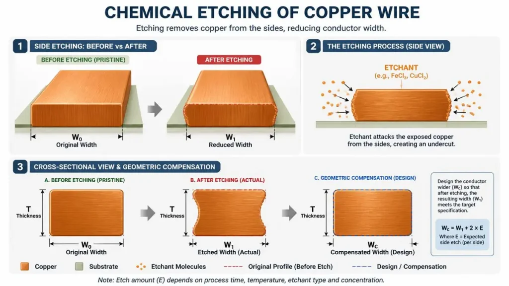
Mechanism of Copper Trace Side Etching (Undercut) and CAM Geometric Compensation Principle
The table below establishes the minimum design guidelines required by Shenzhen Hongda Circuit Technology Co., Ltd. to guarantee reproducible trace structures without bridging or excessive line-width erosion:
| Finished Copper Weight (oz/ft²) | Nominal Copper Thickness (mil / μm) | Minimum Trace Width (mil / μm) | Minimum Air Gap / Spacing (mil / μm) | Suggested Etch Compensation (mil / μm) |
|---|---|---|---|---|
| 4 oz | 5.6 mil / 140μm | 8.0 mil / 200μm | 10.0 mil / 254μm | 2.0 mil / 50μm |
| 6 oz | 8.4 mil / 210μm | 12.0 mil / 305μm | 14.0 mil / 355μm | 3.5 mil / 88μm |
| 10 oz | 14.0 mil / 350μm | 18.0 mil / 457μm | 22.0 mil / 558μm | 5.0 mil / 127μm |
| 15 oz | 21.0 mil / 525μm | 25.0 mil / 635μm | 30.0 mil / 762μm | 7.0 mil / 178μm |
| ≥ 20 oz | ≥ 28.0 mil / ≥ 700μm | Contact Shenzhen Hongda Engineering Team for Advanced Custom Review | ||
Advanced Pad and Plated Via Geometries
Electroplating copper into high-power through-holes significantly reduces the final finished hole diameter. To prevent barrel fractures and ensure uniform plating deposition:
- Drilling Aspect Ratio Limits: For multilayers incorporating thick internal layers, the mechanical drilling aspect ratio must be capped below 8:1 to ensure fluid dynamics equilibrium during acid copper plating cycles.
- Via Wall Plating Thickness: While standard boards require 0.8 mil to 1.2 mil of hole-wall copper, Shenzhen Hongda enforces a minimum of 2.0 mil to 2.5 mil for high-power applications, driving via thermal failure rates down to near zero percent.
- Thermal Relief Pad Configurations: Direct connections to thick copper planes act as localized heat sinks during SMT assembly. Layouts must feature 4-point thermal reliefs with extended web widths (≥ 20 mil) to prevent cold solder joint defects during reflow profiles.
3. Critical Process Engineering & Shenzhen Hongda Mitigation Defenses
Subtractive production configurations often cause severe track erosion and uneven profile distribution when applied to heavy clads. 2026 advanced manufacturing relies on integrated chemical and mechanical modifications.
The Threat of Planar Step-Heights and Soldermask Voids
When fine control lines (e.g., 2 oz) are processed immediately adjacent to heavy current paths (e.g., 20 oz) on the same layer via step-plating or embedded copper routines, a steep vertical topography step-height is introduced. Standard Liquid Photoimageable (LPI) soldermask spray systems fail to adequately coat these sharp 90-degree corners. Due to fluid surface tension, the mask thins out over the top corners while trapping air pockets along the trace roots, forming soldermask voids. Under high-voltage operational stress, these enclosed voids collect moisture and chemistry residues, sparking copper dendrite growth and subsequent catastrophic dielectric breakdown.
Shenzhen Hongda Process Defenses
To eliminate these multi-layer failure modes, our production facility deploys three advanced manufacturing measures:
- High-Resin Vacuum-Assisted Multi-Stage Lamination: We select specialized prepregs with extremely high resin mass fractions (66% to 72% resin contents) combined with optimized high-vacuum multi-stage press profiling. This forces the liquid epoxy resin directly into the large subterranean gaps between thick traces, eliminating air traps before full cross-linking thermal cure.
- Multi-Pass Screen Printing with Dry Film Layer Encapsulation: We replace basic single-pass spray applications with automated multi-pass screen printing utilizing high-viscosity formulations. For extreme profile steps, we overlay a solid dry-film soldermask laminate under pressure, guaranteeing a continuous insulation boundary layer of at least 0.8 mil at every corner tip.
- High-Velocity Oscillating Spray Differential Etching: By implementing high-pressure, oscillating chemical spray manicures alongside proprietary organic passivators, we neutralize lateral acid activity, achieving an etch factor (Fe ≥ 4.0) that produces near-vertical trace walls.
4. Thermomechanical Validation: Displacing Legacy Equations with IPC-2152
Historically, design engineers computed copper trace current limits using empirical charts derived from the legacy IPC-2221A standard. However, when applied to advanced multi-layer thick copper structures, this math produces dangerous under-predictions.
The Shortcomings of IPC-2221A Math Models
The standard legacy formula approaches trace ampacity via a highly simplified equation:
I = 0.048 · ΔT^{0.44} · A^{0.725}
Where I is current (Amperes), ΔT is temperature rise (°C), and A is the trace cross-sectional area (mil²). This legacy model was derived from simplified empirical testing on single-layer boards suspended in mid-air decades ago. It fails to account for modern multilayer board dynamics:
- Variable thermal conductivity coefficients of specialized high-reliability resin matrices (K-factor values).
- The potent heat-sinking effect provided by buried ground and power planes.
- The immense contrast in thermal dissipation efficiency between open outer layers and enclosed inner-core copper lines.
Relying on IPC-2221A typically leads to oversized layouts on outer layers, which wastes spatial footprint, or severely bottlenecked inner layers that over-heat due to a lack of safe derating.
Implementing Modern IPC-2152 Multi-Variable Modeling
Shenzhen Hongda Circuit Technology Co., Ltd. conducts thermal profile assessments utilizing the modern IPC-2152 standard (Standard for Determining Current Carrying Capacity in Printed Board Design). This methodology evaluates the entire material layout framework:
I = K · ΔTα · Wβ · Thγ
The operational exponents (K, α, β, γ) adapt dynamically based on finished board thickness, base laminate composition, and copper plane coverage densities. This high-fidelity model enables our engineering department to safely optimize trace footprints, achieving dense power routing while guaranteeing operation remains within certified thermal boundaries.
Once your thermal model is validated, the next critical step is understanding how these engineering choices translate into actual board cost. Read our Cost Analysis: 4-Layer Heavy Copper PCB for Power Supply Units to see how copper weight, laminate selection, and panel utilization affect your per-board pricing.
5. Advanced Substrate Selection & Thermal Interface Control
Integrating large blocks of structural copper within a multi-layer board drastically alters the global thermomechanical behavior of the composite board.
CTE Mismatch and Inter-Layer Delamination Vulnerabilities
Copper exhibits a linear coefficient of thermal expansion (CTE) of roughly 17 ppm/°C. In contrast, standard low-cost FR4 base materials expand along their vertical Z-axis at a rate of 50 to 70 ppm/°C before hitting their glass transition temperature (Tg). During lead-free reflow heating peaks (reaching 260°C) or continuous thermal cycling, this large differential expansion creates localized shear stress concentrations. This mechanical stress can result in interlayer delamination, trace separation, or internal microvia barrel fractures.
2026 High-Reliability Base Laminate Portfolios
To eliminate thermomechanical shear failures, Shenzhen Hongda enforces strict raw material quality standards, selecting high-performance laminates for all heavy copper assemblies:
- High-Tg / Low Z-CTE Industrial Laminates (e.g., Shengyi S1000-2M, Isola 370HR): Featuring a Tg ≥ 180°C, a Z-axis CTE restricted below 40 ppm/°C, and an excellent decomposition temperature (Td ≥ 350°C), this material group provides dependable performance for industrial power conversion applications at an optimal cost point.
- Aerospace-Grade Polyimide Resin Systems (e.g., Arlon 85N): Engineered with a Tg ≥ 250°C, this class provides excellent structural stability under prolonged extreme thermal exposure, making it the choice for demanding military, aerospace, and down-hole energy systems.
Surface Finish Optimization for High Heat Capacity Assemblies
Because thick copper traces function as localized heat sinks, they rapidly draw heat away from solder joints during assembly. Selecting a compatible surface finish is critical to maintaining proper solder wetting and joint integrity:
- Electroless Nickel Immersion Gold (ENIG): Shenzhen Hongda’s primary recommended finish. It delivers an flat, highly solderable pad topography that resists copper oxidation over multiple reflow thermal profiles.
- Lead-Free Hot Air Solder Leveling (LF HASL): Highly suited for robust, high-current connections where excellent solder wetting and structural joint strength under high mechanical load are paramount.
- Organic Solderability Preservatives (OSP): A cost-efficient option for straightforward power paths, provided assembly profiles utilize precise flux control and consistent pre-heating parameters.
Accelerate Your Power Designs with Shenzhen Hongda
Engineering a reliable heavy copper or EXTREME copper PCB requires careful balancing of mechanical layout choices and chemical processing capabilities. Simple online calculators and outdated design rules often lead to board failures, manufacturing defects, or costly over-engineering.
By engaging the engineering team at Shenzhen Hongda Circuit Technology Co., Ltd. early in your design cycle, you ensure your high-power layout is fully optimized for manufacturing. We analyze your thermal requirements, select the ideal material stack-ups, and apply precise process controls to deliver robust, high-performance PCBs tailored for demanding AI, industrial, and aerospace infrastructure.
FAQs
How does your factory control the “Undercut” and line width tolerances for 4 oz+ Heavy Copper PCBs?
For extreme heavy copper fabrication (4 oz up to 200 oz), lateral chemical etching inevitably causes an Undercut. To counter this, our engineering team utilizes an advanced Etch Factor / Etch Compensation system during the CAM stage. We strictly optimize chemical pooling and conveyor speeds in our horizontal etching lines, ensuring that line width tolerances and minimum spacing meet IPC Class 3 high-reliability standards for AI server power distribution networks (PDN).
Soldermask voids are a common defect in thick copper boards. How do you prevent dendrite growth and voltage breakdown?
The massive vertical step-height of heavy copper tracks frequently traps air, leading to Soldermask Voids, which can trigger Dendrite Growth and high-voltage breakdown under continuous high-power AI workloads. To eliminate this, we implement a multi-pass screen printing process combined with vacuum laminating. This guarantees 100% soldermask encapsulation over the copper encapsulation profile, maintaining optimal dielectric breakdown voltage across all layers.
Do you calculate the ampacity and temperature rise based on IPC-2152, and what base materials do you use?
Yes, we completely abandon outdated IPC-2221A empirical formulas and utilize IPC-2152 multi-variable 3D thermal conductivity matrices to precisely calculate safe ampacity and temperature rise ($\Delta T$). To mitigate the CTE mismatch between heavy copper and dielectric layers—which causes delamination—we exclusively source high-reliability, High-Tg and low Z-axis CTE laminates (such as Shengyi S1000-2M, Isola 370HR, or Arlon 85N for aerospace-grade stability).
How do you solve the “thermal sinking effect” during SMT reflow soldering on thick copper multi-layer boards?
Heavy copper layers act as massive thermal sinks, absorbing heat rapidly and causing cold solder joints or component misalignment during SMT assembly. In our DFM review, we mandate and optimize Thermal Relief Pads to thermally isolate component pins while maintaining high current capacity. Additionally, our state-of-the-art SMT lines feature customized, multi-zone reflow ovens with extended thermal profiles designed specifically for high-thermal-mass assemblies.
What surface finishes do you recommend for heavy copper PCBs to ensure excellent solderability?
For high-mass heavy copper boards, we primarily recommend ENIG (Electroless Nickel Immersion Gold) or LF HASL (Lead-Free Hot Air Solder Leveling). Since heavy copper requires longer dwell times in solder baths, our ENIG process ensures a perfectly flat, non-oxidizing surface with a reliable intermetallic compound (IMC) layer, capable of withstanding multiple high-temperature reflow cycles without degrading solder joint integrity.
About Author
David Chen https://www.linkedin.com/in/pcbcoming
David Chen boasts an extensive professional background in PCBA manufacturing, PCBA testing, and PCBA optimization, with specialized expertise in high-precision PCBA fault analysis and rigorous PCBA reliability testing. The author has worked with high-layer-count server PCB fabrication, ultra-low-loss backplane stackups, and thermo-mechanical reliability optimization for AI infrastructure projects involving 112G and 224G PAM4 architectures. Skilled in complex circuit design and cutting-edge advanced PCB manufacturing processes, he delivers solutions that elevate product durability and performance across industrial applications. His technical articles focusing on PCBA manufacturing workflows and testing methodologies are widely cited by industry peers, research institutions, and technical platforms, solidifying his reputation as a recognized technical authority in the global circuit board manufacturing sector.