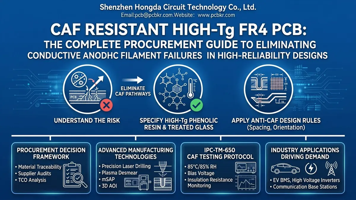
CAF Resistant High-Tg FR4 PCB: The Complete Procurement Guide to Eliminating Conductive Anodic Filament Failures in High-Reliability Designs
When a field-returned EV battery management system shorts out after eighteen months of operation, the root cause is rarely obvious. More often than not, the failure originates inside the board itself—along the glass-resin interface of a multilayer PCB where copper ions have silently migrated under the combined stress of high voltage, humidity, and thermal cycling. This phenomenon, known as Conductive Anodic Filament (CAF), represents one of the most expensive hidden risks in modern electronics procurement.
For procurement teams and design engineers sourcing High-Tg FR4 PCBs for automotive, industrial, and telecom applications, CAF resistance is no longer a secondary specification. It is a primary reliability gate that determines whether your product survives its warranty period—or triggers a costly recall. At Shenzhen Hongda Circuit Technology Co., Ltd. —a global manufacturer serving 5G-Advanced, 6G, semiconductor, automotive, and industrial markets with multilayer capabilities up to 60 layers (scaling to 80 layers in 2026)—we have observed that buyers who treat CAF resistance as an afterthought consistently face higher total cost of ownership. Those who build it into their procurement framework from day one protect both their margins and their reputations.
This guide is written specifically for the PCB procurement decision chain: design engineers defining material specifications, sourcing managers evaluating supplier capabilities, quality engineers auditing manufacturing controls, and program managers assessing lifetime reliability risk. We will walk through the electrochemistry of CAF formation, the material science behind anti-CAF High-Tg FR4 laminates, the design rules that interrupt filament growth, the advanced manufacturing technologies that enforce these rules at scale, and the application-specific requirements driving demand across EV BMS, high-voltage inverters, and communication base stations.
What Is CAF and Why High-Tg FR4 PCB Procurement Teams Can’t Ignore It
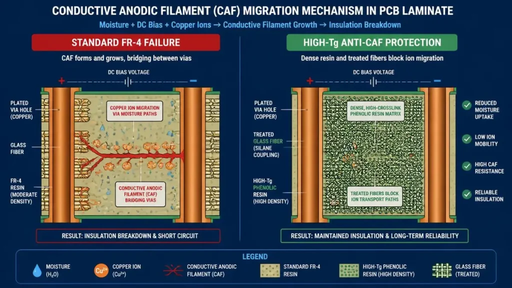
CAF Resistant High-Tg FR4 PCB – Conductive Anodic Filament Migration Mechanism Diagram
The Electrochemical Mechanism Behind Conductive Anodic Filament Formation
Conductive Anodic Filament (CAF) is an electrochemical migration failure mechanism that occurs when copper ions dissolve from a positively biased conductor (the anode), travel through moisture-laden pathways along the glass fiber–resin interface inside the PCB laminate, and deposit onto a negatively biased conductor (the cathode). Over time—weeks, months, or years—this deposited copper extends into a continuous conductive bridge that reduces insulation resistance, creates leakage current paths, and eventually causes catastrophic short circuits.
The process requires three concurrent conditions: electrical bias (voltage difference between conductors), moisture (humidity ingress into the laminate), and a pathway (typically along glass fibers where resin bonding has degraded). In dense multilayer boards with fine-pitch vias and high-voltage nets, these conditions align with alarming frequency. Standard FR-4 materials—with glass transition temperatures (Tg) of 130–140°C—provide only moderate resistance to this degradation, particularly after repeated lead-free reflow cycles that stress the resin-glass bond.
The financial impact is severe. A single CAF-related field failure in an automotive BMS can trigger warranty claims, diagnostic labor, replacement logistics, and brand damage that dwarfs the original PCB unit cost. For procurement professionals, the lesson is clear: CAF resistance must be specified at the material selection stage, not discovered during failure analysis.
Why Standard FR-4 Falls Short in High-Humidity, High-Voltage Environments
Standard FR-4 laminates use dicyandiamide (DICY)-cured epoxy systems that soften significantly when operating temperatures approach or exceed the Tg threshold. When resin softens, the mechanical bond between glass fiber and epoxy weakens, creating micro-gaps that admit moisture. Once moisture penetrates these interfaces, the electrochemical cell forms and ion migration begins. In applications operating above 48V DC—such as EV powertrains, solar inverters, and telecom power supplies—this risk accelerates dramatically.
High-Tg FR4 materials, with Tg values of 170°C and above, maintain mechanical rigidity across wider temperature ranges. This structural stability preserves the glass-resin bond integrity that is the first line of defense against CAF initiation. However, Tg alone is insufficient. The resin chemistry, glass treatment, and manufacturing process controls must work in concert to deliver reliable anti-CAF PCB performance over a 10- to 15-year service life.
High-Tg FR4 Material Science: The Foundation of CAF Resistant PCB Manufacturing
Resin System Chemistry — Phenolic-Cured vs DICY-Cured for Anti-CAF Performance
Not all High-Tg FR4 materials deliver equal CAF resistance, and procurement teams who specify only “Tg > 170°C” without addressing resin chemistry leave a critical vulnerability uncontrolled. The curing agent used in the epoxy formulation fundamentally determines how the resin interacts with glass fibers under thermal and electrical stress.
DICY-cured epoxy systems are the industry standard for general-purpose FR-4. They offer good processability and cost efficiency but exhibit weaker long-term resistance to electrochemical migration. Under sustained humidity and bias, DICY-cured resins are more prone to hydrolytic degradation at the fiber-resin interface—the exact boundary where CAF propagates.
Phenolic-cured epoxy systems, by contrast, form denser cross-linked polymer networks that resist moisture ingress and maintain bond integrity under thermal cycling. Research from laminate manufacturers and independent testing laboratories consistently shows that phenolic-cured High-Tg FR4 materials outperform DICY-cured equivalents in IPC-TM-650 Method 2.6.25 CAF resistance testing, often maintaining insulation resistance above 10⁷ Ω for 1,000+ hours under 85°C/85% RH/bias conditions. For procurement teams sourcing boards for automotive or industrial applications, specifying phenolic-cured High-Tg FR4 is not an upgrade—it is a risk mitigation requirement.
At Hongda Circuit, our material qualification process requires laminate suppliers to provide documented CAF test data per IPC-TM-650, Method 2.6.25C, with test durations matched to the end-use environment. For high-voltage automotive programs, we qualify materials at 100–1,000V DC bias for 596–1,000 hours—well beyond the standard 100V baseline.
CAF-Resistant Glass Fiber Cloth — The Physical Barrier Against Conductive Anodic Filament
While resin chemistry controls moisture absorption and bond stability, the glass fiber architecture determines whether a migration pathway exists in the first place. Standard woven glass fabrics contain bundles of fibers with interstitial gaps that can act as capillary channels for moisture and ion transport. CAF-resistant glass fiber cloth addresses this through two mechanisms:
- Tightened weave architecture: Reduced bundle spacing limits the continuous channels along which copper ions can migrate. Spread glass styles improve resin coverage and eliminate the large air pockets that accelerate filament growth.
- Silane surface treatment: Advanced glass fabrics receive chemical treatments that promote covalent bonding between the glass surface and the epoxy resin. This treatment strengthens the fiber-resin interface—the precise boundary that CAF exploits—making it significantly more difficult for moisture to penetrate and ions to travel.
The combination of a high-Tg phenolic-cured resin system and silane-treated CAF-resistant glass fiber creates a dual-defense laminate structure. The resin resists moisture absorption and thermal softening; the glass fabric interrupts the physical pathways. For buyers evaluating High-Tg FR4 PCB material selection, requesting documentation of both resin chemistry and glass treatment is a non-negotiable step in supplier qualification.
Material Protection Mechanism — How Resin and Glass Work Together to Reduce Filament Formation
In a properly specified anti-CAF laminate, the protection is synergistic. The high-Tg resin maintains dimensional stability during assembly reflow (peak temperatures of 240–260°C for lead-free soldering) and field operation, preventing the micro-cracking that creates initial pathways. The treated glass fabric ensures that even if localized stress occurs, the fiber-resin boundary remains too well-bonded to support continuous ion migration.
This material advantage translates directly to design freedom. Engineers can use tighter via pitches and higher layer counts—essential for compact EV BMS and dense base station designs—without accepting elevated CAF risk. However, material selection is only the first 80% of the battle. The remaining 20% depends on design rules and manufacturing controls.
Anti-CAF PCB Design Rules Every Procurement Engineer Should Verify Before Sourcing
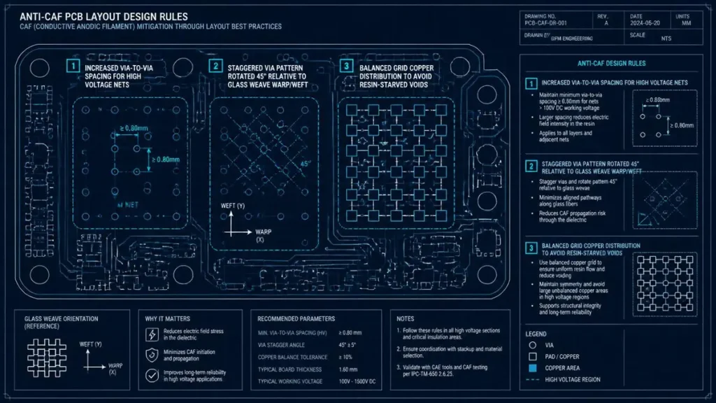
Anti-CAF PCB Layout Design Rules for High-Tg FR4 PCBs
Via-to-Via Spacing Guidelines for High Voltage PCB Layouts
Via-to-via spacing is the most critical geometric variable in CAF risk management. The shorter the distance between two vias at different potentials, the higher the electric field gradient (V/mil) and the faster electrochemical migration proceeds. In high-voltage designs—particularly EV BMS applications where battery pack voltages reach 400V to 800V DC—spacing decisions directly determine whether CAF develops within the product lifetime.
Industry guidance and empirical test data support the following spacing framework:
| Application Voltage | Minimum Via-to-Via Spacing (Same Net) | Recommended Spacing (Different Potentials) |
|---|---|---|
| < 48V DC | 0.25 mm | 0.50 mm |
| 48–200V DC | 0.50 mm | 0.75 mm |
| 200–500V DC | 0.75 mm | 1.00 mm |
| > 500V DC | 1.00 mm | 1.50 mm+ |
These values exceed IPC-2221 minimums, which represent baseline safety clearances rather than CAF prevention thresholds. Procurement teams should verify that their PCB supplier’s DFM review process flags via spacing violations against application-specific CAF criteria—not just generic IPC clearance rules.
An equally important but frequently overlooked factor is via orientation relative to glass weave. CAF propagates along glass fiber directions (warp and weft). When vias align in a straight line parallel to the weave, they create an ideal migration highway. Rotating via pairs by 10° to 45° relative to the board edge forces any potential filament to cross multiple fiber bundles, dramatically slowing propagation. At Hongda Circuit, our CAM engineering team performs weave-orientation analysis during pre-production DFM reviews for all High-Tg multilayer programs.
Copper Grid Layout Strategies to Minimize Electrochemical Migration
Copper distribution across PCB layers affects both thermal performance and CAF risk. Uneven copper density creates localized resin-rich and resin-starved regions during lamination. Resin-starved areas—where insufficient epoxy flows to fully encapsulate glass fibers—leave voids and dry spots that become pre-existing CAF pathways.
Grid copper layout (also called hatched or cross-hatched copper pours) addresses this by distributing copper more uniformly than solid pours while maintaining electromagnetic shielding and thermal conductivity benefits. For procurement teams, the key design rules to enforce are:
- Maintain minimum 60% copper distribution balance across any layer pair to ensure even resin flow during lamination.
- Avoid isolated copper slivers near high-voltage nets, which concentrate electric fields and create localized stress points.
- Use rounded corners on all copper features in high-voltage regions; sharp 90° corners generate field concentrations that accelerate dielectric breakdown and CAF initiation.
- Delete non-functional pads on inner layers while maintaining design-rule spacing. This increases the effective copper-to-copper distance without altering electrical connectivity.
When reviewing supplier capabilities, ask whether their stack-up engineering team simulates resin flow and copper balance using specialized lamination modeling software. At Hongda Circuit, we validate every High-Tg stack-up for resin fill capacity against copper density before releasing to production—a step that prevents the inner-layer voids and delamination risks commonly associated with heavy copper + thin prepreg combinations.
Trace Separation Rules for High Humidity Operating Conditions
Trace-to-trace spacing on outer and inner layers must account for both creepage (surface distance along the board) and clearance (straight-line distance through air or insulation). In humid environments, surface moisture reduces effective creepage distance, making generous spacing essential.
For High-Tg FR4 PCB design rules targeting high-humidity environments:
- Increase trace spacing by 20–30% above IPC-2221B minimums for applications where condensation is possible.
- Separate high-voltage nets onto dedicated layer pairs with generous clearances to signal layers.
- Avoid long parallel runs between traces at different potentials; where parallel routing is unavoidable, insert grounded shield traces.
- Apply teardrops at trace-to-pad and trace-to-via junctions to reduce mechanical stress concentrations that can seed micro-cracks.
These rules add minimal board area cost but provide substantial insurance against field failures. Procurement teams should include them as explicit requirements in fabrication drawings and verify compliance through supplier DFM reports.
Advanced PCB Manufacturing Technologies That Guarantee CAF Resistance
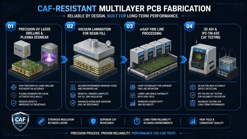
Manufacturing Process Flow for CAF Resistant High-Tg FR4 PCBs
Design rules specify intent; manufacturing equipment and process control deliver the outcome. For buyers evaluating High-Tg FR4 PCB suppliers, understanding which manufacturing technologies directly impact CAF resistance enables more rigorous supplier audits and smarter sourcing decisions.
Precision Laser Drilling and Desmear Control for Clean Hole Walls
Mechanical drilling is the most common source of glass-resin interface damage in multilayer PCBs. Aggressive drilling parameters—excessive spindle speed, worn drill bits, or improper feed rates—generate heat that thermally degrades resin and tears glass fibers rather than cutting them cleanly. The resulting rough hole walls and fiber pull-out create the exact micro-fractures where CAF initiates.
UV laser drilling systems address this by ablating material with minimal mechanical stress. For microvias and high-density interconnect (HDI) structures, laser drilling produces cleaner hole walls with superior resin-glass bond preservation. For through-holes in thick High-Tg multilayers, advanced CNC drilling platforms with real-time wear monitoring and optimized speed/feed parameters reduce fiber damage significantly.
Equally critical is the desmear process, which removes resin smear from hole walls after drilling. Inadequate desmear leaves residues that block electroless copper adhesion; excessive desmear attacks the glass-resin interface itself, creating the very pathways CAF exploits. Modern plasma desmear systems using tailored gas chemistries (CF₄/O₂ blends) offer precise control that mechanical wet-desmear processes cannot match for High-Tg materials.
At Hongda Circuit, our manufacturing line integrates precision mechanical drilling with UV laser microvia capability and plasma desmear processing. For High-Tg programs, drill parameters are optimized per laminate type, and bit wear is monitored via automated tool life tracking to ensure every hole meets surface roughness specifications that support long-term CAF resistance.
mSAP Process and Automated Optical Inspection for High-Density Anti-CAF Designs
As via pitches shrink and layer counts increase—particularly in 112G/224G PAM4 high-speed backplanes and AI server PCBs where Hongda Circuit specializes—traditional subtractive etching struggles to maintain the trace geometry precision required for reliable spacing. The modified semi-additive process (mSAP) enables finer line/space resolution (down to 30/30 µm and below) with more uniform copper profiles, ensuring that designed spacing values are achieved consistently in production.
Uniform trace geometry matters for CAF resistance because variable etching can create copper slivers and neck-downs that concentrate electric fields. mSAP eliminates these artifacts by building traces up from a thin seed layer rather than etching them down from thick foil.
Following fabrication, 3D Automated Optical Inspection (AOI) verifies that trace spacing, via alignment, and copper distribution match design intent. Modern AOI systems capture height and volumetric data, detecting spacing violations that 2D systems miss—particularly critical in High-Tg multilayers where inner-layer defects are not visible after lamination.
Hongda Circuit deploys mSAP for ultra-fine-pitch High-Tg designs and integrates 3D AOI at multiple production stages to ensure that anti-CAF design rules are manufactured as specified, not merely designed.
IPC-TM-650 Method 2.6.25 CAF Testing Protocol Implementation
No amount of design rigor or manufacturing precision substitutes for empirical verification. IPC-TM-650 Method 2.6.25 is the industry-standard test for evaluating CAF resistance, exposing test coupons to 85°C and 85% relative humidity with applied DC bias voltage while monitoring insulation resistance over 596 hours (25 days).
For procurement teams, the critical questions to ask suppliers are:
- Do you perform CAF testing in-house or through a third-party laboratory?
- What bias voltages and test durations do you use for qualification? (Standard is 10–100V DC for 596 hours; high-voltage automotive programs should demand 100–1,000V DC for 596–1,000 hours.)
- Which test coupon designs do you use? (IPC-9253 for X-Y axis via-to-via evaluation; IPC-9254 for Z-axis layer-to-layer evaluation.)
- What is your pass/fail criteria? (Insulation resistance must remain above 10⁷ Ω throughout testing.)
- Do you retain production samples for ongoing reliability monitoring?
At Hongda Circuit, CAF testing is integrated into our material qualification and production monitoring protocols. We maintain test coupons from every High-Tg material lot and perform periodic HAST (Highly Accelerated Stress Test) and THB (Temperature-Humidity-Bias) validation to ensure that our manufacturing process does not introduce the ionic contamination or process residues that accelerate CAF growth.
Industry Applications Driving Demand for CAF Resistant High-Tg FR4 PCBs
EV Battery Management Systems — High Voltage Compact Layout Challenges
Electric vehicle battery management systems (BMS) represent the most demanding application environment for High-Tg FR4 PCBs with CAF resistance. These boards must manage 400V to 800V DC battery pack voltages in enclosures where temperature cycling, vibration, and humidity are constant realities. The compact form factors required for under-hood and battery pack integration force dense via arrays and fine-pitch components, minimizing the spacing that would otherwise reduce CAF risk.
For procurement teams sourcing BMS PCBs, the failure cost is existential. A CAF-induced short in a BMS can trigger false state-of-charge readings, thermal runaway propagation failures, or complete system shutdowns. The material and design specifications must therefore include:
- Phenolic-cured High-Tg FR4 (Tg ≥ 170°C, preferably 180°C) with documented CAF test data
- Via-to-via spacing of 0.75 mm minimum for high-voltage nets
- Staggered via patterns rotated 45° relative to board edges
- Conformal coating as secondary moisture protection (never a substitute for laminate CAF resistance)
- Full IPC-TM-650 Method 2.6.25 qualification at automotive-relevant bias voltages
Hongda Circuit supplies multilayer High-Tg PCBs to tier-1 automotive suppliers, with manufacturing controls aligned to IATF 16949 quality management requirements and material traceability protocols that support PPAP submission.
High Voltage Inverters — Electrical Stress and Conductive Feature Separation
Solar inverters, industrial motor drives, and EV traction inverters operate at elevated voltages with continuous switching transients that create both DC bias and AC ripple stress. The combination of high electrical potential and rapid voltage transitions accelerates electrochemical migration beyond what steady-state DC models predict.
In these applications, anti-CAF PCB design rules for high voltage inverters must address:
- Increased internal layer clearances: High-voltage nets should be routed on dedicated inner layers with 1.0 mm+ spacing to adjacent layers.
- CTI-rated materials: Comparative Tracking Index (CTI) ≥ 600V materials prevent surface tracking that can complement internal CAF failures.
- Slot and groove isolation: Non-plated slots between high-voltage and low-voltage regions increase creepage distance without increasing board size.
- Thermal management integration: Heat-generating components (IGBTs, MOSFETs) must be thermally isolated from high-voltage traces to prevent localized temperature spikes that degrade resin bonds.
Procurement teams should verify that their PCB supplier understands the difference between standard high-voltage clearance rules and CAF-specific spacing requirements. A board that passes hipot testing at time-zero can still fail in the field if CAF pathways develop over months of humidity exposure.
Communication Base Stations — Dense Layouts and Long-Term Reliability
5G-Advanced and emerging 6G infrastructure demand PCBs that combine high-speed signal integrity with long-term environmental resilience. Base station equipment operates outdoors or in uncontrolled indoor environments for 10–15 years, exposed to humidity, temperature extremes, and airborne contamination.
The dense via arrays required for high-speed backplanes and RF modules create ideal conditions for CAF if material selection and manufacturing controls are inadequate. High-Tg FR4 PCB for communication base stations must therefore balance:
- Low Dk/Df for signal integrity at 112G/224G PAM4 data rates
- High Tg (≥ 170°C) for thermal stability in sealed outdoor enclosures
- CAF-resistant laminate construction for decade-long service life
- Controlled impedance uniformity that is not compromised by resin degradation over time
Hongda Circuit’s capability in 60-layer backplanes (scaling to 80 layers) with 112G/224G PAM4 support positions us to address both the electrical performance and the CAF reliability requirements of next-generation telecom infrastructure.
How to Evaluate a High-Tg FR4 PCB Supplier for CAF Resistance — A Procurement Decision Framework
Material Traceability and Laminate Qualification Documentation
The first checkpoint in supplier evaluation is material provenance. Reputable suppliers maintain direct relationships with laminate manufacturers (Isola, Panasonic, TUC, Shengyi) and can provide:
- Lot-specific material datasheets showing Tg, Td, CTE, moisture absorption, and CAF resistance
- IPC-4101 slash sheet compliance documentation
- Third-party CAF test reports per IPC-TM-650 Method 2.6.25
- Certificate of conformance for every production lot
Beware suppliers who cannot name the specific laminate grade or who substitute “equivalent” materials without engineering approval. CAF resistance varies significantly between materials that share the same nominal Tg.
Manufacturing Equipment Audit — From Drilling to Ion Chromatography
A capable High-Tg FR4 PCB manufacturer for CAF-sensitive applications should demonstrate:
| Process Step | Required Capability | CAF Relevance |
|---|---|---|
| Drilling | Precision CNC with tool life monitoring; UV laser for microvias | Clean hole walls prevent fiber-resin damage |
| Desmear | Plasma desmear with process control | Avoids glass-resin interface attack |
| Lamination | Vacuum lamination with programmable pressure/temperature profiles | Ensures complete resin cure and wetting |
| Plating | Electroless + electrolytic copper with ionic contamination control | Prevents residual salts that accelerate CAF |
| Inspection | 3D AOI + cross-sectional analysis | Verifies spacing and hole wall quality |
| Testing | Ion chromatography + IPC-TM-650 CAF testing | Validates cleanliness and long-term reliability |
During supplier audits, request to see process control records, equipment calibration certificates, and actual CAF test data from recent production lots. A supplier who treats CAF testing as a special request rather than a standard protocol is not prepared for high-reliability programs.
Total Cost of Ownership Analysis for CAF Resistant PCB Programs
High-Tg CAF-resistant laminates typically cost 15–25% more than standard FR-4. Specialty materials with enhanced CAF resistance may carry a 20–50% premium. However, in the context of total program cost, this material uplift usually represents only 1–5% of the total PCBA cost—while potentially eliminating field failure risks that carry warranty, recall, and reputation costs orders of magnitude higher.
Procurement teams should structure their RFQ evaluations to include:
- Unit PCB cost: Material, labor, overhead, and margin
- Qualification cost: First article inspection, CAF testing, reliability validation
- Risk-adjusted failure cost: Estimated field failure rate × cost per failure (warranty, replacement, logistics, brand impact)
- Supplier engineering support: DFM review quality, stack-up optimization, test program design
The lowest unit-cost supplier rarely delivers the lowest total cost of ownership when CAF-related field failures are factored into the equation. At Hongda Circuit, we work with procurement teams to model these trade-offs explicitly, ensuring that material and process investments align with application risk profiles.
Frequently Asked Questions: What Procurement Teams Ask When Sourcing CAF Resistant High-Tg FR4 PCBs
How do I know if my application actually needs CAF-resistant High-Tg FR4, or if standard FR-4 is sufficient?
If your product operates above 48V DC, experiences humidity exposure above 60% RH, uses multilayer construction with 6+ layers, or requires a service life exceeding five years, standard FR-4 presents unacceptable CAF risk. High-Tg FR4 (Tg ≥ 170°C) with documented CAF resistance becomes essential. For EV BMS, high-voltage inverters, and outdoor telecom equipment, it is non-negotiable. A practical rule: if your maximum operating temperature exceeds 100°C or your board undergoes lead-free reflow, specify High-Tg. If voltage and humidity coexist in the end-use environment, specify CAF-resistant High-Tg.
What specific material documentation should I request from my PCB supplier to verify CAF resistance?
Request four documents: (1) the laminate manufacturer’s datasheet showing Tg (DSC method), Td, moisture absorption, and CAF resistance claims; (2) IPC-4101 slash sheet compliance certificate; (3) IPC-TM-650 Method 2.6.25 test results for the specific material grade, including test voltage, duration, and final insulation resistance values; and (4) a Certificate of Conformance for the production lot your boards will be built from. If your supplier cannot provide these, they are not controlling material risk—they are transferring it to you.
Can conformal coating prevent CAF, or do I still need special laminate materials?
Conformal coating protects board surfaces from moisture and contamination, but CAF develops inside the laminate along internal glass-resin interfaces. Coating cannot prevent moisture that entered during manufacturing or migrates through board edges from initiating internal electrochemical migration. Coating is a valuable secondary defense, but it does not replace CAF-resistant laminate material, proper spacing design, and manufacturing cleanliness. Specify coating in addition to—not instead of—anti-CAF material and design practices.
How does via placement and orientation actually affect CAF risk in production boards?
CAF propagates preferentially along glass fiber directions (warp and weft). When vias at different potentials align in a straight line parallel to the weave, they create a continuous migration highway with minimal resistance. Rotating via pairs by 10° to 45° relative to the board edge forces any potential filament to cross multiple glass bundle intersections, increasing propagation resistance by an order of magnitude or more. Staggering vias between layers rather than stacking them directly prevents straight-line Z-axis pathways. These rules cost nothing in material but provide substantial reliability returns.
What is the difference between HAST, THB, and IPC-TM-650 CAF testing—and which should I specify?
HAST (Highly Accelerated Stress Test) uses elevated temperature and humidity (typically 130°C/85% RH) with pressure to accelerate failure mechanisms in days rather than months. It is excellent for rapid material screening but may not perfectly correlate with field conditions. THB (Temperature-Humidity-Bias) operates at milder conditions (85°C/85% RH) for longer durations and provides a closer approximation of real-world aging. IPC-TM-650 Method 2.6.25 is the formal standard for CAF resistance evaluation, specifying 85°C/85% RH with applied bias for 596 hours minimum using standardized coupon geometries (IPC-9253, 9254, 9255, 9256). For procurement, specify IPC-TM-650 Method 2.6.25 as the baseline qualification requirement, with extended durations (1,000 hours) and elevated bias voltages (100–1,000V DC) for high-voltage automotive or industrial programs.
Conclusion: Building CAF Resistance Into Your Procurement DNA
Conductive Anodic Filament is not a theoretical risk—it is a documented failure mode that has destroyed product launches, triggered automotive recalls, and eroded supplier relationships. The procurement teams who avoid these outcomes share one characteristic: they treat CAF resistance as a first-class specification rather than a footnote.
This means specifying phenolic-cured High-Tg FR4 with CAF-resistant glass fiber. It means enforcing via spacing, copper distribution, and trace separation rules that exceed generic IPC minimums. It means auditing supplier manufacturing equipment for drilling precision, desmear control, and inspection capability. And it means demanding empirical proof—IPC-TM-650 test data, ion chromatography reports, and production sample retention—not just promises.
At Shenzhen Hongda Circuit Technology Co., Ltd. , we have built these capabilities into our standard operating procedures for High-Tg multilayer programs. From 60-layer backplanes for 5G infrastructure to compact multilayers for EV BMS, our manufacturing platform combines advanced equipment, material science expertise, and rigorous testing protocols to deliver boards that survive the environments where CAF thrives.
If your next program involves high voltage, high humidity, dense layout, or long service life requirements, do not leave CAF resistance to chance. Contact our engineering team at www.pcbkr.com for a DFM review, material recommendation, and CAF qualification strategy tailored to your application.
Shenzhen Hongda Circuit Technology Co., Ltd. is a global manufacturer of high-precision multilayer PCBs, HDI, rigid-flex, high-frequency, and high-speed backplanes, serving the 5G-Advanced, 6G, semiconductor, automotive, and industrial markets. With multilayer capabilities up to 60 layers (80-layer mass production scaling in 2026) and full support for 112G/224G PAM4 signal integrity, PCBHongda Circuit delivers the material expertise and manufacturing quality that high-reliability applications demand.
About Author
David Chen https://www.linkedin.com/in/pcbcoming
David Chen boasts an extensive professional background in PCBA manufacturing, PCBA testing, and PCBA optimization, with specialized expertise in high-precision PCBA fault analysis and rigorous PCBA reliability testing. The author has worked with high-layer-count server PCB fabrication, ultra-low-loss backplane stackups, and thermo-mechanical reliability optimization for AI infrastructure projects involving 112G and 224G PAM4 architectures. Skilled in complex circuit design and cutting-edge advanced PCB manufacturing processes, he delivers solutions that elevate product durability and performance across industrial applications. His technical articles focusing on PCBA manufacturing workflows and testing methodologies are widely cited by industry peers, research institutions, and technical platforms, solidifying his reputation as a recognized technical authority in the global circuit board manufacturing sector.