Copper Base & DTP PCB Material Specification Guide: An Engineering Whitepaper
Executive Summary:
A copper base printed circuit board (copper-substrate MCPCB) represents the pinnacle of metallic thermal management, comprising a circuit foil layer, a high-density ceramic-filled polymer dielectric, and a solid copper base layer (typically C1100, bulk conductivity approximately 385 W/m·K). While implementing a copper bulk substrate eliminates global heat-sinking bottlenecks, real-world thermo-mechanical reliability is governed by dielectric joint interfaces, precise pedestal planarization, and trace-etch geometric compensation. This whitepaper establishes quantitative Design-for-Manufacturability (DFM) boundaries and structural guidelines required to mitigate infant field failures in high-power AI server infrastructure, GaN power stages, and dense laser diode arrays.
1. Thermo-Mechanical Fundamentals: Copper vs. Aluminum Core
Specifying a copper base over standard aluminum (such as 5052 or 6061 alloys) becomes mandatory when operating power densities cross the critical threshold of 30 W/cm², or when component junctions are sensitive to thermal throttling. The engineering justification relies on two primary physical metrics:
Global Thermal Dissipation
With a bulk thermal conductivity of approximately 385 W/m·K, pure copper transfers thermal energy roughly 3 times faster than aluminum alloys (130 to 170 W/m·K), drastically shrinking the transient thermal response window.
Coefficient of Thermal Expansion (CTE) Mitigation
- C1100 Copper Core: 16.5 to 17.0 ppm/°C
- Aluminum Core (5052 alloy): 22.0 to 23.0 ppm/°C
- Ceramic Component Substrates (AlN / Al2O3): 5.0 to 7.0 ppm/°C
During rapid temperature differential (ΔT) power cycling, the severe CTE mismatch between aluminum and brittle ceramic packages induces intense interfacial shear stress on the solder joints, leading to micro-cracking and premature open circuits. Copper aligns much closer to the ceramic baseline, multiplying solder joint fatigue life by up to 4 times.
2. Advanced Material Characterization & Sourcing Matrix
Generic “high-thermal” callouts on fabrication drawings yield unpredictable line card behavior. Material specification must delineate between standard metal-clad coatings (MCPCB) and multi-layer structural prepregs.
| Material Performance Tier | Bulk Dielectric Conductivity (k) | Multi-Layer Prepreg (For High-Layer Backplanes) | Single/Double-Sided MCPCB Castings | Target Application Context |
|---|---|---|---|---|
| Tier 1: Standard | 2.0 – 3.0 W/m·K | Ventec VT-4B1 | Shengyi SFM1, Bergquist T-Clad | Mid-power industrial SMPS, LED drivers |
| Tier 2: High Thermal | 4.0 – 4.2 W/m·K | Ventec VT-4B5, Laird Tlam PP | Shengyi SFM3 | Automotive EV powertrains, dense buck-boost stages |
| Tier 3: Extreme Thermal | 8.0+ W/m·K | Arlon 92HP (High-Polymer Layered PP) | Bergquist HT-06003, Ventec VT-4B7 | AI server backplanes, phase-shifted full-bridge modules |
Design Note: Ultra-high conductivity dielectrics (8.0+ W/m·K) achieve performance by packing the polymer matrix tightly with ceramic micro-particles. This increases material brittleness and alters fluid dynamics during lamination. Designers must account for lower resin flow, requiring optimized press cycles to prevent microscopic voiding along heavy copper trace walls.
3. Direct Thermal Path (DTP) & Pedestal Planarization Mechanics
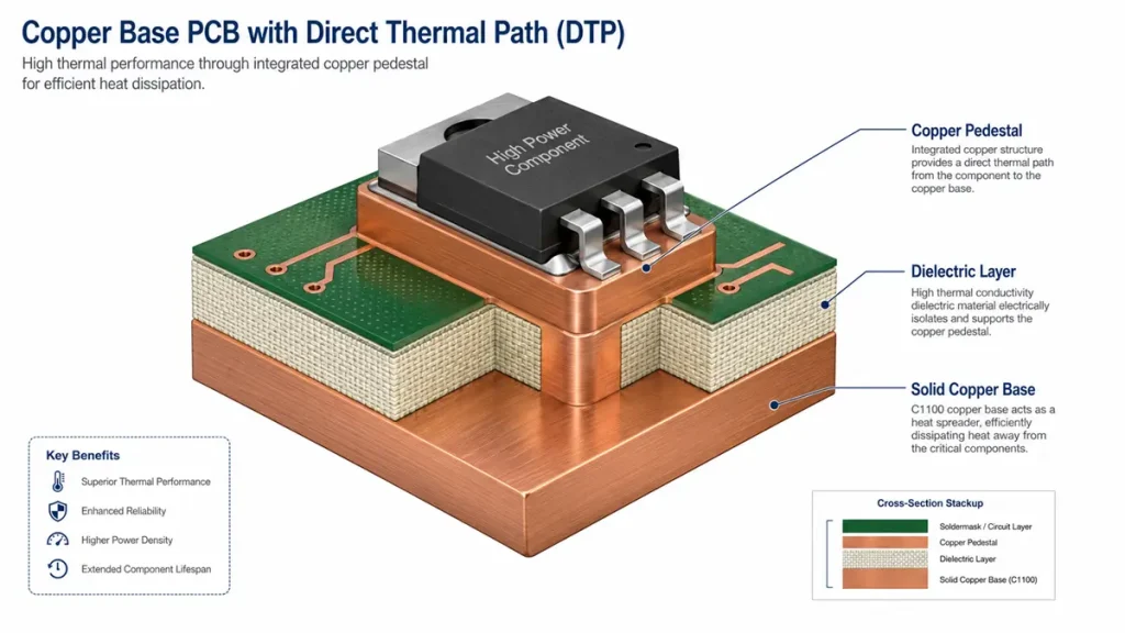
Copper Base PCB with Direct Thermal Path (DTP) Technology
For extreme power densities (exceeding 100 W/cm²), even a high-performance 4.0 W/m·K dielectric layer introduces an unacceptable thermal barrier. Direct Thermal Path (DTP) architecture resolves this by executing a thermoelectric separation.
Instead of a uniform coating, the C1100 base is selectively CNC-milled or coin-formed to generate a localized, integrated copper pedestal that extends upward through the dielectric zone. The dielectric layer is mechanically removed at this interface, resulting in a 0 mil dielectric intersect directly underneath the component’s center thermal pad. The thermal pad of the power component is soldered directly onto this pedestal, while its electrical pins are soldered onto the isolated circuit traces.
Copper Base PCB Material Crucial DFM Boundaries for DTP:
Step Height Flatness (Pedestal Surface Profile): The top surface of the copper pedestal must sit strictly coplanar with the adjacent circuit layer traces. The target specification must state: Step Height Coplanarity ±0.025 mm (±1 mil absolute upper limit). If the pedestal is too high, it causes tilt or component “tombstoning” during reflow; if it sits too low, a thick solder joint forms, introducing an unintended thermal interface resistance.- Solder Mask Encroachment: Liquid Photoimageable (LPI) solder mask behaves unpredictably when passing over the sharp vertical step of a DTP pedestal. To prevent solder mask chipping, peeling, or pooling at the step root, maintain a minimum clearance of 6 mils (0.15 mm) from the pedestal edge to the active solder mask opening.
4. Unmasking Advanced Fabrication Failures & DFM Constraints
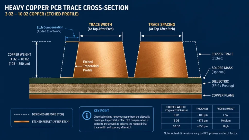
Heavy Copper PCB Trace Cross-Section & Etch Compensation
Heavy Copper Etch Profiles & Undercut Compensation
Deploying 3 oz to 10 oz and greater outer copper circuits to handle high current densities forces fabricators into prolonged chemical etching cycles, inducing a trapezoidal trace cross-section due to lateral undercutting. To counteract this, the fabricator must adjust Gerber trace geometries prior to exposure. Layout designers must adhere to strictly scaled trace width and trace separation rules:
- For 3 oz Finished Copper: Minimum Line Width / Spacing = 8 mils (0.20 mm)
- For 5 oz Finished Copper: Minimum Line Width / Spacing = 12 mils (0.30 mm)
- For 10 oz Finished Copper: Minimum Line Width / Spacing = 25 mils (0.63 mm)
Failing to respect these limits expands the risk of circuit necking or un-etched copper bridge shorts.
Asymmetric Warp, Panel Twist, and “Copper Cracking”
Single-sided copper MCPCB stack-ups inherently represent unbalanced asymmetric configurations. Pure copper exhibits an aggressive thermal response during 260°C lead-free reflow profiles. Large, unbroken isolation voids in the top copper foil trigger localized stress gradients, bowing the panel outward.
Furthermore, because the solid copper core extracts heat rapidly, it establishes a massive thermal gradient (ΔT) between the component junction and the substrate base. This localized thermal shock creates high shear strain at the corners of plated through-holes (PTH) and at the base anchor points of DTP pedestals. Over extended power cycling, this stress manifests as copper corner cracking. All single-sided layouts should maintain uniform copper balancing across the top layer. Use cross-hatched copper flooding in non-signal areas rather than leaving wide, open dielectric islands.
5. Quantitative Thermal Calculations & Engineering Case Study
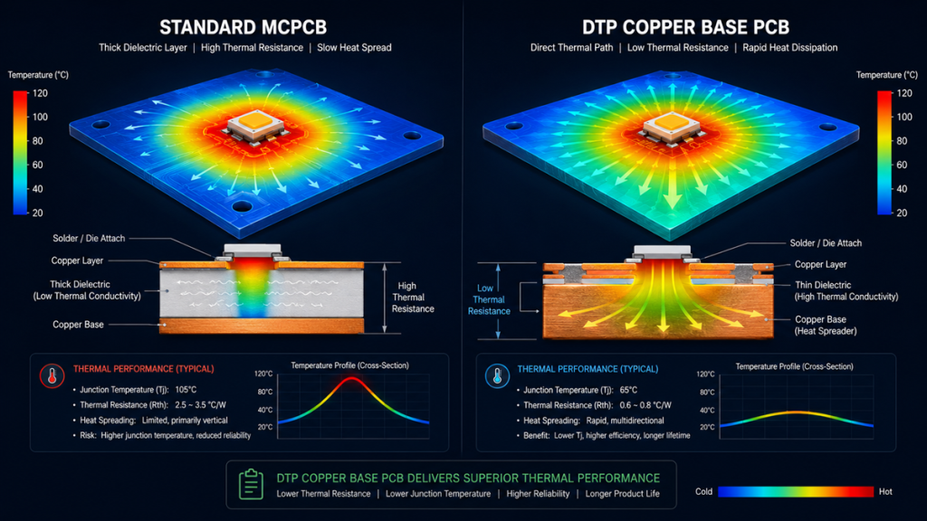
Copper Base PCB Material with Direct Thermal Path (DTP)
System-Level Thermal Resistance Modeling
Designing a thermal solution purely based on the bulk conductivity (k) listed on a laminate datasheet is a critical system architecture error. Real junction temperature rise is governed by system-level thermal resistance, calculated as:
Rth = d / (k * A)
Where: d is the dielectric layer thickness, k is the dielectric material’s bulk conductivity, and A is the total active thermal interface area.
In real-world applications, a thin, high-performance 50 µm dielectric layer with a moderate rating of 3.0 W/m·K yields a lower operating junction temperature than a thick 100 µm dielectric layer marketing a higher 4.0 W/m·K rating, because it slashes the total conduction path length (d) by half.
Case Study: High-Power GaN Converter Optimization
- The Challenge: A customer experienced premature field failures on an AI server power stage driven by discrete GaN FETs mounted on a standard aluminum MCPCB (2.0 W/m·K). Under full load (85 W dissipation per block), the GaN junction temperature spiked to 138°C, causing periodic thermal shutdown and micro-fractures in the SAC305 solder joints due to the severe aluminum-to-ceramic CTE variance.
- The Solution: The design was migrated to a C1100 Copper Base DTP Structure utilizing a 75 µm Bergquist HT-06003 dielectric for the adjacent gate-drive circuitry. The GaN thermal pad was directly soldered to a ±1 mil planarized copper pedestal.
- The Result: The direct metal-to-metal thermal path dropped the interface thermal resistance to near zero, lowering the operational junction temperature to 84°C (a 54°C net reduction) while matching the ceramic package CTE to prevent joint cracking.
6. Master Technical DFM Specification Checklist
Incorporate these exact technical parameters into your fabrication drawing notes before releasing Gerbers for production quotes:
| Parameter Category | Specific Technical Metric | Industry DFM Standards & Structural Constraints |
|---|---|---|
| Base Metal Substrate | Copper Grade & Thickness Callout | C1100 Grade (Oxygen-Free, Pure Copper); Thickness options: 0.8mm, 1.0mm, 1.5mm, 2.0mm, 3.2mm |
| Dielectric Insulation | Manufacturer Brand Name & Thickness | Specify explicitly: e.g., Bergquist HT-06003 (3.0 W/m·K / Thickness: 75 µm) or Ventec equivalent |
| Circuit Foil Layer | Finished Outer Copper Mass | 1 oz, 2 oz, 3 oz, up to 10 oz and greater. (Trace-to-space spacing must scale proportionally with copper mass). |
| Core Architecture | Mechanical Layout Mode | Single-Sided MCPCB, Double-Sided with Resin-Isolated PTH, or Direct Thermal Path (DTP) |
| Pedestal Precision | DTP Step Height Profiling | Milling depth control: ±0.025 mm (±1 mil absolute upper limit) |
| Dielectric Integrity | Hi-Pot Breakdown Voltage Limit | Factory Electrical Testing: Mandatory greater than or equal to 2.0 kV AC or greater than or equal to 3.0 kV DC for 60-second dwell |
| Mechanical Profile | Edge Finishing & Singularization | CNC Mechanical Routing mandatory for thick copper; V-Scoring strictly prohibited if core thickness exceeds 1.5mm |
| Surface Finish | Component Interface SMT Plating | ENIG (Electroless Nickel Immersion Gold) mandatory for coplanar SMT thermal pads; OSP restricted to cost-sensitive legacy zones |
Technical Resources & DFM Engineering Support
📥 Download Comprehensive Design Kit: Advanced Metal Core Layout Rules (PDF)
Includes IPC-2152 current-versus-temperature charts tailored for heavy copper matrices up to 10 oz, multi-layer stack-up templates, and custom DRC rulesets for Altium Designer and Cadence Allegro.
For a definitive, interactive DFM validation of your current layout—including step height verification, pedestal clearance audits, and trace etch compensation calculations—submit your Gerber archive directly to our staff at sales@pcbkr.com.
FAQs
Our design includes a Direct Thermal Path (DTP) structure. How does your facility ensure pedestal co-planarity with the surrounding circuit traces?
DTP yield rates directly impact assembly efficiency. Procurement must verify if the supplier can guarantee a ±0.025 mm (±1 mil) milling precision to prevent soldering voids or solder paste bridging, which are common causes of design rejection.
For extreme-conductivity dielectrics (8.0+ W/m·K), how do you mitigate voiding during the lamination process?
High-thermal dielectrics contain high ceramic filler percentages, making lamination difficult. Procurement needs to verify that the supplier uses controlled press cycles and can provide C-SAM (Scanning Acoustic Microscopy) reports to ensure the dielectric layer is free of micro-voids.
What are your minimum line width/spacing limits for heavy copper (3 oz+) designs?
Heavy copper induces significant lateral undercutting. Procurement must obtain the supplier’s etch compensation table to ensure their manufacturing capabilities meet the DRC (Design Rule Check) requirements of the layout, preventing late-stage production failures.
Can you provide long-term reliability data (e.g., power cycling tests) for AI server or automotive power applications?
“Functional” is not the same as “durable.” Procurement should request stress analysis reports on copper cracking during 260°C lead-free reflow or extended power cycling, ensuring compliance with standards such as IATF 16949 for automotive-grade reliability.
How do you control warpage for single-sided copper base PCBs?
Asymmetric stack-ups are highly prone to warping. Procurement needs to confirm if the supplier employs balanced copper fill strategies (cross-hatching) or specific fixture solutions to ensure the board remains flat during SMT assembly, preventing line stops caused by warped panels.
About Author
David Chen https://www.linkedin.com/in/pcbcoming
David Chen boasts an extensive professional background in PCBA manufacturing, PCBA testing, and PCBA optimization, with specialized expertise in high-precision PCBA fault analysis and rigorous PCBA reliability testing. The author has worked with high-layer-count server PCB fabrication, ultra-low-loss backplane stackups, and thermo-mechanical reliability optimization for AI infrastructure projects involving 112G and 224G PAM4 architectures. Skilled in complex circuit design and cutting-edge advanced PCB manufacturing processes, he delivers solutions that elevate product durability and performance across industrial applications. His technical articles focusing on PCBA manufacturing workflows and testing methodologies are widely cited by industry peers, research institutions, and technical platforms, solidifying his reputation as a recognized technical authority in the global circuit board manufacturing sector.