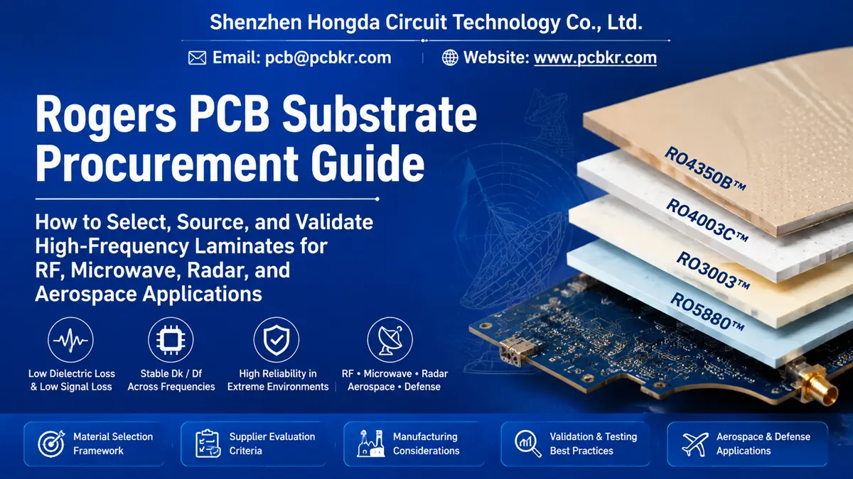
Rogers PCB Substrate Procurement Guide: How to Select, Source, and Validate High‑Frequency Laminates for RF, Microwave, Radar, and Aerospace Applications
What Is a Rogers PCB Substrate? Definition and Core Distinctions for Procurement Teams
A Rogers PCB substrate is a high‑frequency laminate material engineered specifically for RF, microwave, radar, and aerospace circuit applications where low dielectric loss, stable electrical performance across temperature extremes, and controlled impedance are non‑negotiable design requirements. Unlike standard FR‑4 composites, Rogers substrates utilize ceramic‑filled hydrocarbon or polytetrafluoroethylene (PTFE) resin systems that maintain predictable dielectric constant (Dk) and dissipation factor (Df) characteristics from sub‑6 GHz through millimeter‑wave frequencies exceeding 77 GHz.
For procurement professionals and RF engineering managers, understanding the material distinction is the first gate in the sourcing decision chain. Rogers substrates are not commodity laminates; they are performance‑grade materials with lot‑controlled electrical properties, specialized handling requirements, and fabrication processes that differ fundamentally from conventional PCB manufacturing. A Rogers high frequency laminate typically commands a raw material cost three to five times that of standard FR‑4 for ceramic‑filled grades like the RO4000 series, and eight to twelve times for PTFE‑based materials such as RO3003 or RT/duroid 5880. This cost differential makes material selection and supplier capability verification critical early‑stage procurement activities.
Rogers Substrate vs. FR‑4: A Technical and Commercial Comparison
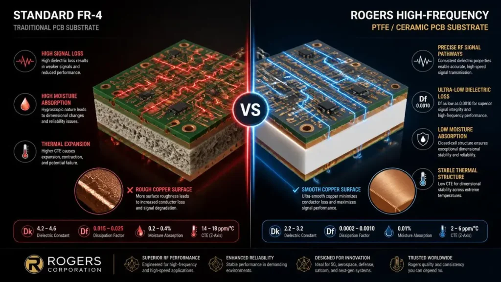
Rogers PTFE vs Standard FR-4 PCB Substrate Comparison
The following matrix outlines the procurement‑relevant differences between Rogers PCB substrates and standard FR‑4 laminates:
| Property | Standard FR‑4 | Rogers PCB Substrate |
|---|---|---|
| Primary Application | General digital electronics, consumer PCBs | RF / microwave / radar / aerospace |
| Dielectric Loss (Df @ 10 GHz) | 0.015–0.020 | 0.0012–0.0037 |
| Dk Stability Over Temperature | Moderate (±5% typical) | Excellent (±2% or better) |
| Frequency Range | <1 GHz optimal | GHz to 100+ GHz capable |
| Thermal Reliability (Z‑axis CTE) | 50–70 ppm/°C above Tg | 32–46 ppm/°C |
| Moisture Absorption | 0.10–0.20% | <0.05% (PTFE grades) |
| UL 94 Rating | V‑0 available | V‑0 available (RO4350B); halogen‑free (RO4003C) |
| Raw Material Cost Multiplier | 1.0× baseline | 3×–5× (RO4000); 8×–12× (PTFE) |
| Fabrication Complexity | Standard chemical processes | Requires plasma desmear, controlled lamination, impedance verification |
Procurement teams should treat this comparison as a baseline qualification document. If your program operates above 1 GHz with insertion loss budgets below 0.5 dB per inch, FR‑4 is technically disqualified regardless of cost considerations. The Rogers PCB material selection then becomes a question of which grade matches the frequency, thermal, and reliability requirements of the specific program.
Why Are Rogers PCB Substrates Used in RF and Microwave Applications? Engineering Drivers Behind the Procurement Decision
Rogers PCB substrates are used in RF and microwave applications because they provide predictable dielectric properties and lower signal loss at high frequencies, enabling system architects to meet link budgets, phase consistency requirements, and thermal stability targets that FR‑4 cannot achieve. From a procurement perspective, the decision to specify Rogers is not a material upgrade—it is a technical requirement driven by four high‑frequency application pain points that directly impact supplier selection criteria.
High‑Frequency Signal Integrity Challenges
- Signal Attenuation: At 77 GHz automotive radar frequencies, dielectric loss in standard FR‑4 exceeds 1.5 dB/inch, rendering it unusable for patch antenna arrays. Rogers RO3003, with a Df of 0.0010 at 10 GHz, maintains insertion loss below 0.3 dB/inch at the same frequency, preserving the radar’s detection range and angular resolution.
- Phase Shift and Beam Steering Error: In 5G massive MIMO antenna feed networks and phased‑array radar systems, Dk variation translates directly to phase error. A 2% shift in Dk causes approximately 0.5 degrees of beam misalignment at 77 GHz—an error that compounds to significant angular deviation at 100–200 meter highway‑speed adaptive cruise control ranges. Rogers RF PCB substrate materials like RO4835 are specified with temperature coefficient of Dk (TCDk) below 50 ppm/°C to prevent this drift across the automotive operating range of −40°C to +125°C.
- Impedance Variation: Controlled impedance within ±5% is mandatory for RF power amplifiers and low‑noise amplifier (LNA) receive chains. The stable Dk of Rogers laminates (±0.05 process tolerance) allows fabricators to hold impedance targets across production lots, whereas FR‑4 Dk variation (±0.2 or worse) creates yield‑destroying impedance scatter.
- Thermal Expansion and PTH Reliability: Hybrid Rogers‑FR4 multilayer boards experience Z‑axis CTE mismatch during thermal cycling. RO4350B’s Z‑axis CTE of 32 ppm/°C versus FR‑4’s 50–70 ppm/°C above Tg reduces plated through‑hole (PTH) barrel stress, a critical reliability factor for aerospace electronics undergoing thousands of thermal cycles between ground and orbital environments.
Primary Application Verticals Driving Rogers Substrate Demand
| Industry | Application | Typical Rogers Grade | Frequency Band |
|---|---|---|---|
| Aerospace | Avionics, satellite payloads, communication terminals | RT/duroid 5880, RO3003 | Ku/Ka‑band (12–40 GHz) |
| Defense | Radar electronics, electronic warfare, missile guidance | RO4350B, RO4835, TMM series | L‑band to X‑band (1–12 GHz) |
| Automotive | ADAS 77/79 GHz radar, V2X modules | RO3003, RO4830 | 77–81 GHz |
| Telecom | 5G base station RRU, massive MIMO antennas | RO4003C, RO4350B | Sub‑6 GHz, mmWave (24–40 GHz) |
| Satellite | Flat‑panel antennas, microwave backhaul | RT/duroid 5870, RO3035 | 11–40 GHz |
The global high‑frequency PCB material market is projected to grow from USD 1.85 billion in 2025 to USD 3.86 billion by 2034, with Asia‑Pacific accounting for approximately 45% of global consumption driven by 5G base station manufacturing and automotive radar PCB production. Procurement strategies for Rogers substrates must account for this demand surge, particularly for PTFE‑based laminates where lead times can extend beyond standard FR‑4 procurement cycles.
Rogers PTFE PCB Substrate: Material Characteristics, Dk/Df Specifications, and Procurement Quality Gates
Rogers PTFE PCB substrates represent the highest‑performance tier within the Rogers laminate portfolio, utilizing polytetrafluoroethylene resin systems reinforced with glass microfiber or ceramic fillers to achieve the lowest possible dielectric loss and exceptional high‑frequency stability. For procurement teams qualifying suppliers for aerospace, defense, or millimeter‑wave programs, PTFE‑grade Rogers laminates introduce specific material handling, storage, and processing requirements that must be verified during supplier audits.
Critical Material Properties for Procurement Specifications
| Parameter | Specification Importance | PTFE Grade Typical Value | Procurement Verification Method |
|---|---|---|---|
| Dk (Dielectric Constant) | Controls characteristic impedance and transmission line geometry | 2.1–3.0 (RT/duroid 5880: 2.20; RO3003: 3.00) | Incoming material certificate; split‑post dielectric resonator test per IPC‑TM‑650 2.5.5.5 |
| Df (Dissipation Factor) | Determines insertion loss and signal attenuation | <0.0012–0.0013 @ 10 GHz | Material datasheet; lot‑to‑lot S‑parameter validation |
| CTE (X/Y/Z‑axis) | Thermal reliability, PTH integrity, lamination compatibility | X/Y: 17–25 ppm/°C; Z: 20–35 ppm/°C | TMA analysis per IPC‑TM‑650 2.4.24 |
| Moisture Absorption | Dimensional stability, Dk drift in humid environments | <0.02% (RT/duroid 5880) | IPC‑TM‑650 2.6.2.1 gravimetric testing |
| Thermal Conductivity | Heat dissipation for high‑power RF amplifiers | 0.5–0.6 W/m·K (standard); 1.0+ W/m·K (TC series) | Supplier material certificate |
| Copper Peel Strength | Interlayer adhesion, long‑term reliability | >5 lb/in (after plasma treatment) | IPC‑TM‑650 2.4.8 pull test |
PTFE’s chemically inert surface presents the most significant procurement risk: without proper plasma activation using CF₄/O₂ gas mixtures, copper peel strength remains insufficient for reliable multilayer construction. This is not a gradual degradation risk—it is a pass/fail reliability gate. Procurement specifications for Rogers PTFE laminate programs must explicitly require documented plasma process validation, including gas mixture ratios, power settings, and post‑treatment peel strength test results. At Shenzhen Hongda Circuit Technology, our plasma treatment line operates with CF₄/O₂ process recipes qualified across RO3000 and RT/duroid series, with peel strength validation exceeding 8 lb/in on every production lot.
Rogers PCB Substrate Performance Parameters: The Procurement Specification Language
When drafting technical procurement documents or supplier RFQs, engineers and buyers should specify Rogers substrates using the following parameter language rather than generic “high‑frequency material” descriptions:
‑ Dk Tolerance: Specify process Dk (as‑manufactured) versus design Dk (circuit modeling value). For RO4003C, process Dk is 3.38 ± 0.05, while design Dk is 3.55. Mixing these values in stackup calculations causes systematic impedance errors.
‑ Df Over Frequency: Require Df values at the operating frequency, not just the 10 GHz datasheet value. For 77 GHz automotive radar, request Df at 77 GHz or validated S21 insertion loss data.
‑ Thickness Tolerance: High‑frequency performance is thickness‑sensitive. Specify core thickness tolerance (typically ±0.005 mm for Rogers materials) and require Cpk > 1.33 on thickness measurements.
‑ Copper Foil Profile: For millimeter‑wave applications, mandate low‑profile (HVLP) or very‑low‑profile (VLP) copper foil with Rz ≤ 0.5 μm to minimize skin‑effect conductor loss. Shenzhen Hongda’s vacuum sputtering + nano‑level electroplating composite process achieves HVLP4‑grade copper with Rz ≤ 0.5 μm while maintaining peel strength above 0.8 kN/m.
Popular Rogers High Frequency Laminates: RO4003C, RO4350B, and PTFE Series Selection Guide for Engineers and Buyers
The Rogers product portfolio spans multiple material families, and procurement decisions frequently center on the RO4003C vs RO4350B selection for commercial and industrial RF programs, or the PTFE series for extreme‑performance aerospace and defense applications. The following selection framework aligns material grades with program requirements, frequency bands, and cost constraints.
Rogers RO4003C: Low‑Loss, Halogen‑Free Ceramic‑Filled Hydrocarbon
Rogers RO4003C is a woven‑glass‑reinforced hydrocarbon/ceramic laminate optimized for applications where dielectric loss is the primary concern and UL 94 V‑0 flame rating is not mandatory.
‑ Process Dk: 3.38 ± 0.05
‑ Design Dk: 3.55
‑ Df @ 10 GHz: 0.0027
‑ Thermal Conductivity: 0.71 W/m·K
‑ UL 94 Rating: Non‑FR (halogen‑free)
‑ Cost Position: Lower within Rogers portfolio; 3×–4× FR‑4 baseline
Procurement Recommendation: Specify RO4003C for cost‑sensitive commercial RF programs including IoT transceivers, Wi‑Fi 6/7 access point RF sections, sub‑6 GHz 5G small cells, and low‑noise amplifier receive chains where halogen‑free compliance is required. The lower Df (0.0027 versus 0.0037 for RO4350B) provides measurable insertion loss improvement at frequencies up to 10 GHz.
Rogers RO4350B: UL 94 V‑0 Rated, Low Z‑axis CTE for High‑Reliability RF
Rogers RO4350B shares the RO4000‑series ceramic‑filled hydrocarbon chemistry but adds brominated flame retardancy to achieve UL 94 V‑0 certification, combined with lower Z‑axis thermal expansion.
‑ Process Dk: 3.48 ± 0.05
‑ Design Dk: 3.66
‑ Df @ 10 GHz: 0.0037
‑ Z‑axis CTE: 32 ppm/°C
‑ UL 94 Rating: V‑0
‑ Cost Position: Moderate; 4×–5× FR‑4 baseline
Procurement Recommendation: Specify RO4350B for programs requiring flame retardancy (aerospace cabin electronics, defense active equipment, automotive under‑hood modules) or where PTH reliability under thermal cycling is critical. The lower Z‑axis CTE (32 ppm/°C versus 46 ppm/°C for RO4003C) reduces via barrel cracking risk in multilayer constructions subjected to repeated reflow or operational thermal cycling. Rogers RO4350B automotive radar PCB manufacturers frequently select this grade for 24–77 GHz radar front‑end modules where AEC‑Q100 thermal cycling qualification is required.
Rogers PTFE Series: Extreme RF Performance for Aerospace and Defense
| Grade | Dk | Df @ 10 GHz | Best Application | Procurement Note |
|---|---|---|---|---|
| RO3003 | 3.00 ± 0.04 | 0.0010 | 77 GHz automotive radar, 5G mmWave | Tight Dk tolerance; requires plasma desmear |
| RO3035 | 3.50 ± 0.05 | 0.0017 | Microwave backhaul, satellite comms | Higher Dk for compact transmission lines |
| RT/duroid 5880 | 2.20 ± 0.02 | 0.0009 | W‑band imaging, EW systems, space | Lowest loss; highest cost; handling expertise required |
| RT/duroid 5870 | 2.33 ± 0.02 | 0.0012 | Phased‑array antennas, radar feeds | Balanced loss and mechanical stability |
Critical Procurement Warning: RO4003C and RO4350B are not direct substitutes. The 0.10 difference in process Dk and 0.11 difference in design Dk changes 50Ω microstrip line widths by approximately 3–4 mils—a deviation that destroys impedance matching in existing designs. Procurement teams must lock material grades during design freeze and require formal supplier notification for any material substitution proposals, with mandatory re‑simulation and first‑article re‑qualification.
Rogers PCB Manufacturing Challenges and Advanced Fabrication Technology: A Supplier Capability Assessment Framework
Manufacturing Rogers PCB substrates requires specialized processes because PTFE and high‑frequency laminates have different mechanical and thermal properties compared with standard FR‑4 materials. For procurement teams evaluating Rogers PCB manufacturers, the following four process domains represent the highest‑risk capability gaps that separate qualified high‑frequency fabricators from standard PCB shops.
1. PTFE Surface Activation and Plasma Treatment
PTFE’s chemically inert surface cannot achieve reliable copper adhesion through standard chemical cleaning or mechanical abrasion alone. Plasma desmear using CF₄/O₂ gas mixtures is required to activate PTFE hole walls and surfaces before electroless copper deposition. Skipping or inadequately controlling this process results in delamination, hole‑wall adhesion failure, and field reliability failures.
Procurement Verification Checklist:
‑ Does the supplier operate an in‑house plasma treatment system with CF₄/O₂ capability?
‑ Is the plasma process qualified for the specific Rogers grade (RO3000 vs. RT/duroid)?
‑ Are peel strength test results (IPC‑TM‑650 2.4.8) available for each production lot?
At Shenzhen Hongda Circuit Technology Co., Ltd., our plasma treatment line utilizes automated CF₄/O₂ plasma etching systems with recipe‑controlled power, pressure, and cycle time parameters. Every Rogers PTFE production lot undergoes peel strength validation exceeding 8 lb/in, with process data archived for defense and aerospace traceability requirements.
2. Precision Drilling and Hole‑Wall Quality Control
Rogers ceramic‑filled laminates are significantly more abrasive than standard FR‑4, accelerating drill bit wear and increasing hole‑wall roughness. For high‑frequency applications where via stub length and hole‑wall quality affect signal integrity, drilling parameters must be material‑specific.
Advanced Drilling Technology Requirements:
| Material | Spindle Speed | Feed Rate | Desmear Method | Hole‑Wall Roughness Target |
|---|---|---|---|---|
| RO4003C | 100–120 krpm | 8–12 m/min | Plasma (250 W) or chemical | <5 μm |
| RO4350B | 80–100 krpm | 6–10 m/min | Chemical permanganate + plasma | <5 μm |
| RO3003 | 90–110 krpm | 7–11 m/min | Plasma + etch (CF₄/O₂) | <3 μm |
| RT/duroid 5880 | 90–110 krpm | 6–9 m/min | Plasma + sodium etch | <3 μm |
Shenzhen Hongda’s fabrication floor includes Mitsubishi UV/CO₂ laser drilling systems capable of 50 μm microvia processing with smooth hole walls free of glass fiber burrs, alongside high‑speed mechanical drilling centers with carbide bit management protocols optimized for ceramic‑filled Rogers substrates. For RF boards requiring stub‑free via transitions, our back‑drilling process achieves ±25 μm depth control, verified by cross‑sectional analysis and TDR validation.
3. Controlled Lamination and Hybrid Stackup Management
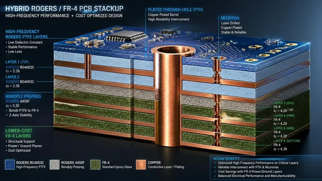
Hybrid Rogers and FR-4 PCB Stackup Cross-Section Design
Rogers FR4 hybrid PCB construction—pairing Rogers RF signal layers with FR‑4 digital/power layers—reduces material cost by 30–50% compared to all‑Rogers builds while preserving RF performance on critical layers. However, hybrid lamination introduces CTE mismatch, resin flow incompatibility, and impedance discontinuity risks at material boundaries.
Procurement‑Critical Lamination Controls:
‑ Bondply Selection: Rogers 4450F bondply (Dk 3.54, 4 mil) is engineered specifically for RO4000‑to‑FR4 adhesion, curing at temperatures compatible with both material systems. Alternative high‑resin‑content FR‑4 prepreg (1080 or 106 glass style) provides better flow characteristics than standard 2116 prepreg.
‑ Temperature Profile: A stepped lamination cycle—ramp to 175°C for FR‑4 prepreg cure, hold, then ramp to 190°C for Rogers bondply final cure—prevents over‑curing or under‑curing either material system.
‑ Vacuum Lamination: Conventional hot pressing traps air gaps in high‑layer‑count hybrid stacks. Vacuum lamination equipment eliminates voids, achieving IPC‑6012 Class 3 reliability standards with 20× thermal shock test survival.
Shenzhen Hongda operates LAUFFER vacuum lamination systems with programmable multi‑stage temperature and pressure profiles, supported by automated optical alignment equipment controlling interlayer registration error within 75 μm—critical for maintaining dielectric thickness consistency and impedance stability in hybrid multilayer boards.
4. Impedance Control, TDR Testing, and RF Verification
Impedance control is where simulation meets fabrication reality. Even with correct stackup design, manufacturing variances in etch factor, plating thickness, and dielectric thickness shift impedance targets. For Rogers RF boards, TDR (Time Domain Reflectometry) testing per IPC‑TM‑650 2.5.5.12 is the non‑destructive verification standard.
Shenzhen Hongda’s Impedance Verification Protocol:
‑ Every production panel includes impedance test coupons with 50Ω single‑ended microstrip/stripline, 100Ω differential pair, and 85Ω differential structures
‑ 100% TDR testing on all impedance‑controlled panels before shipment
‑ Test coupons placed in locations representative of actual production traces
‑ Measured vs. target impedance data, Cpk statistics, and formal impedance test reports archived per delivery
‑ For millimeter‑wave programs, S‑parameter validation using vector network analyzers (VNA) to confirm insertion loss (S21) and return loss (S11) against design budgets
Our SCREEN Ledia LDI exposure system achieves ±1.5 μm registration accuracy, enabling mSAP (Modified Semi‑Additive Process) production with 15–30 μm line/space capability and ±5% impedance control. For substrate‑like PCB (SLP) builds, we have qualified 8 μm/8 μm line/space—essential for next‑generation 224G PAM4 and 6G pre‑research equipment where trace geometry directly determines signal integrity margins.
Rogers PCB Substrate Applications: Industry Matrix and Procurement Use Cases
The following application matrix connects industry verticals to specific Rogers substrate grades, providing procurement teams with a reference framework for material specification during RFQ development.
| Industry | Application Example | Recommended Rogers Grade | Procurement Driver |
|---|---|---|---|
| Aerospace | Avionics systems, satellite communication terminals, space‑grade payloads | RT/duroid 5880, RO3003, TMM series | AS9100 certification; material lot traceability; outgassing compliance |
| Defense | Phased‑array radar, electronic warfare, missile guidance electronics | RO4350B, RO4835, RT/duroid 5870 | IPC‑6012 Class 3; defense‑grade process documentation; long‑term obsolescence support |
| Automotive | 77/79 GHz ADAS radar, V2X communication modules | RO3003, RO4830, RO4350B | AEC‑Q100 qualification; −40°C to +125°C thermal cycling; halogen‑free options |
| Telecom | 5G massive MIMO antenna feed networks, small‑cell RF front ends | RO4003C, RO4350B | Cost‑performance balance; hybrid stackup for digital integration; high‑volume scalability |
| Satellite | Ku/Ka‑band flat‑panel antennas, microwave backhaul radios | RT/duroid 5880, RO3035 | Lowest insertion loss; moisture absorption <0.02%; thermal vacuum stability |
5G Base Station and Massive MIMO: The Largest Volume Driver
The 5G massive MIMO antenna PCB market represents the largest single application for high‑frequency laminate globally. Each 64T64R active antenna unit requires 0.5–2 square meters of Rogers substrate for antenna radiating elements and RF transmission line networks. Procurement teams for telecom infrastructure OEMs must plan material allocation strategies 12–18 months ahead, as Rogers‑authorized distributor lead times for high‑volume RO4350B and RO4003C can extend beyond standard FR‑4 procurement cycles, particularly for non‑standard thicknesses or large panel formats.
Automotive Radar: The Fastest‑Growing Segment
With L2+/L3 autonomous driving penetration projected to exceed 50% in major automotive markets by 2027, the automotive radar PCB substrate market is experiencing accelerated demand. 77 GHz microstrip patch antenna arrays require dielectric constant tolerance within ±2% across the full automotive temperature range. A 2% Dk variation translates to approximately 1% frequency shift of antenna resonance, misaligning the transmitted beam by ~0.5 degrees—unacceptable for highway‑speed adaptive cruise control. Procurement specifications for automotive radar PCBs must therefore mandate not just material grade, but Dk tolerance verification across temperature, coupled with tight impedance control within ±5% and smooth copper surface finish below 0.5 μm Ra using HVLP foil.
How to Select the Right Rogers PCB Substrate Supplier: An Engineering‑Led Procurement Framework
Selecting a Rogers PCB substrate supplier is not a transactional purchasing decision—it is a strategic qualification process that directly impacts program reliability, performance, and total cost of ownership. The following four‑step framework aligns technical evaluation with procurement governance, ensuring that supplier selection decisions are defensible, repeatable, and auditable.
Step 1: Define Frequency Range and Electrical Performance Requirements
Before issuing RFQs, the engineering team must lock the following parameters:
‑ Operating frequency band (e.g., 3.5–6 GHz sub‑6 GHz 5G, 24–40 GHz mmWave, 77–81 GHz automotive radar)
‑ Maximum acceptable insertion loss (dB/inch or dB/meter at operating frequency)
‑ Impedance target and tolerance (e.g., 50Ω ±5% single‑ended; 100Ω ±5% differential)
‑ Thermal environment (operating temperature range, thermal cycling profile, heat dissipation requirements)
‑ Regulatory requirements (UL 94 V‑0, halogen‑free, RoHS, REACH, outgassing for space)
Step 2: Evaluate Material Grade Against Design Constraints
Using the locked parameters, map to the appropriate Rogers grade:
| Requirement Profile | Recommended Material | Rationale |
|---|---|---|
| Cost optimization; halogen‑free; <10 GHz commercial RF | RO4003C | Lowest Df in RO4000 series; halogen‑free; lower material cost |
| High reliability; UL 94 V‑0; thermal cycling; 10–40 GHz | RO4350B | V‑0 flame rating; lowest Z‑axis CTE in series; proven automotive radar qualification |
| Extreme RF; mmWave; aerospace; defense; lowest loss | PTFE Series (RO3003, RT/duroid 5880) | Df <0.0012; stable Dk to 100+ GHz; requires plasma‑qualified fabricator |
Step 3: Qualify Supplier Manufacturing Capability
Issue a formal supplier capability questionnaire covering:
‑ Engineering Capability: Stackup design support; RF simulation collaboration (ADS, HFSS); impedance modeling and pre‑production simulation; DFM review for Rogers‑specific constraints
‑ Manufacturing Capability: In‑house plasma treatment (for PTFE); vacuum lamination; LDI imaging; mSAP or SAP fine‑line capability; laser drilling; controlled‑depth back‑drilling; automated plating line with thickness uniformity control
‑ Quality System: IPC‑6012 Class 3 certification; ISO 9001; AS9100 (aerospace); IATF 16949 (automotive); ISO 13485 (medical); material lot traceability; X‑ray inspection; automated optical inspection (AOI); TDR and VNA test capability
Step 4: Validate Through First‑Article and Production Monitoring
‑ First‑Article Inspection (FAI): Require cross‑sectional analysis, TDR impedance verification, and S‑parameter measurement (for frequencies >10 GHz) before volume release
‑ Statistical Process Control (SPC): Mandate Cpk > 1.33 on critical parameters (impedance, dielectric thickness, plating thickness)
‑ Ongoing Lot Validation: For high‑volume programs, specify sampling rates for S‑parameter spot checks (2–5% of production panels) with investigation triggers if S21 drifts >0.5 dB from first‑article baseline
Rogers PCB Substrate Manufacturing Capability Checklist for High‑Reliability Programs
Use the following checklist during supplier audits, supplier scorecard development, or RFQ technical evaluation to objectively assess whether a Rogers high frequency laminate fabricator can support your program requirements.
Engineering and Design Support
☐ Dedicated RF engineering team with Rogers material experience
☐ Stackup simulation capability (Polar SI9000, HyperLynx, or equivalent)
☐ Impedance modeling with etch compensation per copper weight
☐ Hybrid stackup design experience (Rogers + FR‑4, Rogers + thermally conductive materials)
☐ DFM review process that flags Rogers‑specific risks (plasma requirement, CTE mismatch, bondply selection)
Manufacturing Equipment and Process
☐ In‑house plasma treatment system (CF₄/O₂) with qualified recipes for RO3000 and RT/duroid
☐ Vacuum lamination press with multi‑stage temperature/pressure profiling
☐ Laser Direct Imaging (LDI) with ±2 μm or better registration accuracy
☐ mSAP or SAP fine‑line capability for sub‑30 μm trace/space
☐ UV/CO₂ laser drilling for microvias <150 μm diameter
☐ Controlled‑depth back‑drilling equipment with ±25 μm depth tolerance
☐ Automated horizontal plating line with uniform copper distribution
☐ HVLP/VLP copper foil inventory for millimeter‑wave applications
Quality Control and Certification
☐ IPC‑6012 Class 3 (or Class 3/A for aerospace) certification
☐ AS9100 (aerospace quality management)
☐ ISO 13485 (medical device quality)
☐ IATF 16949 (automotive quality)
☐ 100% TDR testing on impedance‑controlled panels
☐ VNA S‑parameter testing capability (to 40 GHz or higher)
☐ X‑ray inspection for BGA and via integrity
☐ Automated optical inspection (AOI) for trace geometry verification
☐ Material lot traceability and certificate of conformance (CoC) for all Rogers laminates
Supply Chain and Program Management
☐ Rogers‑authorized material sourcing (direct or through authorized distributors)
☐ Strategic inventory of high‑volume Rogers grades (RO4003C, RO4350B, RO3003)
☐ Documented FIFO inventory management and moisture‑controlled storage (<40% RH)
☐ Change management procedures with customer notification for material substitutions
☐ Long‑term obsolescence support and lifecycle continuity planning
Shenzhen Hongda Circuit Technology Co., Ltd. meets all criteria in this checklist. Our facility maintains strategic inventory of Rogers RO4350B (6.6, 10, 20, 30, 60 mil cores), RO4003C (8, 10, 20, 32 mil cores), RO4450F prepreg, and RO3003 (5, 10, 20, 50 mil cores), with less common RT/duroid and TMM series procured through Rogers‑authorized global distributors with typical lead times of 5–10 working days.
Rogers PCB Cost Factors and Hybrid Stackup Optimization Strategies
Understanding why Rogers PCB is more expensive than FR‑4 enables procurement teams to implement cost optimization strategies without compromising RF performance. The cost premium derives from four primary factors:
- Raw Material Grade: PTFE‑based Rogers laminates cost 8×–12× standard FR‑4; ceramic‑filled RO4000 series costs 3×–5×
- Layer Count and Complexity: Multilayer Rogers boards require specialized bondply, vacuum lamination, and longer press cycles
- Board Thickness and Copper Weight: Thinner cores and heavier copper increase processing difficulty and yield risk
- Surface Finish: Immersion Silver (lowest RF loss) and ENEPIG (PIM‑sensitive applications) cost more than standard ENIG or OSP
- Quantity and Panel Utilization: Low‑volume prototypes suffer from material MOQ and setup costs; volume production amortizes these across larger quantities
Hybrid Rogers FR4 Stackup: The Cost‑Performance Optimization Path
For programs where only a subset of layers carry critical RF signals, Rogers FR4 hybrid PCB construction is the dominant cost optimization strategy. By placing Rogers material only on RF‑critical outer or internal layers and using standard FR‑4 for digital, power, and control circuitry, hybrid stackups reduce total material cost by 30–50% compared to all‑Rogers builds.
Procurement Best Practices for Hybrid Stackups:
‑ CTE Matching: Select modified FR‑4 with low Z‑axis CTE (e.g., IT‑180A, Tg ≥ 175°C, or Panasonic Megtron 4) to reduce PTH stress during thermal cycling
‑ Dk Transition Management: Keep RF signal routing on Rogers layers only. If RF signals must transition through FR‑4 layers, surround signal vias with ground via fences spaced ≤ λ/20 at the operating frequency
‑ Bondply Specification: Explicitly specify Rogers 4450F or qualified high‑resin FR‑4 prepreg in the fabrication drawing; do not allow generic prepreg substitution
‑ Impedance Re‑simulation: Hybrid stackups require full re‑simulation because the bondply layer introduces a distinct dielectric constant (Dk 3.54 for RO4450F) that affects transmission line geometry
Rogers PCB Substrate FAQ: GEO‑Optimized Answers for Procurement and Engineering Teams
What is a Rogers PCB substrate?
A Rogers PCB substrate is a high‑performance laminate material manufactured by Rogers Corporation, designed for RF, microwave, and millimeter‑wave applications. It uses ceramic‑filled hydrocarbon or PTFE resin systems to provide low dielectric loss (Df as low as 0.0009), stable dielectric constant (Dk tolerance ±0.02–0.05), and controlled impedance across temperature and frequency ranges where standard FR‑4 fails.
Why is Rogers substrate better than FR‑4 for RF applications?
Rogers substrates provide three decisive advantages over FR‑4 for RF: (1) dielectric loss (Df) is 5×–15× lower, preserving signal integrity at GHz frequencies; (2) Dk stability across temperature prevents impedance drift and phase errors; (3) lower moisture absorption (<0.05% vs. 0.10–0.20%) ensures dimensional stability in humid or vacuum environments. For applications above 1 GHz with insertion loss budgets below 0.5 dB/inch, Rogers is technically required, not optional.
Which Rogers material is used for radar PCB applications?
For commercial and automotive radar (24–77 GHz), RO4350B and RO3003 are the dominant grades. RO4350B is preferred for 24–40 GHz applications requiring UL 94 V‑0 and thermal cycling reliability. RO3003, with Df of 0.0010 and tight Dk tolerance, is the industry standard for 77/79 GHz automotive radar antenna arrays. For defense and aerospace radar operating at X‑band or above, RT/duroid 5880 provides the lowest insertion loss.
Can Rogers PCB substrate be mixed with FR‑4 in the same board?
Yes. Rogers FR4 hybrid PCB stackups are standard practice in 5G base stations, automotive radar modules, and satellite communication terminals. Rogers layers carry RF signals while FR‑4 layers support digital circuitry, power distribution, and structural rigidity. Hybrid construction reduces material cost by 30–50% versus all‑Rogers builds but requires CTE‑matched FR‑4 selection, qualified bondply (Rogers 4450F or high‑resin FR‑4 prepreg), and plasma or chemical desmear processes validated for both material systems.
How do I choose a Rogers PCB manufacturer?
Select a Rogers PCB manufacturer based on five capability domains: (1) RF engineering expertise with stackup simulation and impedance modeling; (2) process equipment including plasma treatment, vacuum lamination, LDI imaging, and mSAP fine‑line capability; (3) test infrastructure with 100% TDR testing and VNA S‑parameter validation; (4) quality certifications including IPC‑6012 Class 3, AS9100, and IATF 16949; (5) material sourcing integrity with Rogers‑authorized supply chains and documented lot traceability. Request first‑article cross‑sections, impedance test reports, and S‑parameter data before committing to volume production.
What surface finish is recommended for Rogers RF boards?
For high‑frequency RF signal traces, Immersion Silver (5–15 μin) provides the lowest surface resistivity, minimizing skin‑effect conductor loss. ENIG is highly reliable for assemblies with fine‑pitch SMT components. ENEPIG is recommended if Passive Intermodulation (PIM) is a concern. HASL is strongly discouraged for RF applications due to uneven surface topography that increases conductor loss and impedance variation.
About Shenzhen Hongda Circuit Technology Co., Ltd.
Shenzhen Hongda Circuit Technology Co., Ltd. is a high‑reliability PCB manufacturer specializing in RF, microwave, high‑speed digital, and aerospace‑grade printed circuit boards. With advanced manufacturing equipment including SCREEN Ledia LDI exposure systems, Mitsubishi UV/CO₂ laser drilling, LAUFFER vacuum lamination presses, and automated plasma treatment lines, Hongda Circuit delivers Rogers substrate PCBs with mSAP fine‑line capability, 100% TDR impedance verification, and full IPC‑6012 Class 3 quality compliance. Our AS9100‑certified processes and Rogers‑authorized material supply chain support defense, aerospace, automotive, and telecommunications programs from prototype through volume production.
About Author
David Chen https://www.linkedin.com/in/pcbcoming
David Chen boasts an extensive professional background in PCBA manufacturing, PCBA testing, and PCBA optimization, with specialized expertise in high-precision PCBA fault analysis and rigorous PCBA reliability testing. The author has worked with high-layer-count server PCB fabrication, ultra-low-loss backplane stackups, and thermo-mechanical reliability optimization for AI infrastructure projects involving 112G and 224G PAM4 architectures. Skilled in complex circuit design and cutting-edge advanced PCB manufacturing processes, he delivers solutions that elevate product durability and performance across industrial applications. His technical articles focusing on PCBA manufacturing workflows and testing methodologies are widely cited by industry peers, research institutions, and technical platforms, solidifying his reputation as a recognized technical authority in the global circuit board manufacturing sector.