Rapid Rogers PCB Prototype & Instant Manufacturing Quote
Accelerate 24‑48 Hour RF Turnaround with Precision Impedance Control & Direct Factory Pricing
Rogers 4350B PCB cheap high‑frequency hardware development does not mean compromising performance, as transitioning an RF circuit from simulation to physical reality is fraught with speed and precision bottlenecks. Engineering and procurement teams often encounter severe friction: prototype turnaround times extending into weeks, strict RF impedance requirements failing first‑article audits, and inflated unit costs for low‑volume runs that strain development budgets.
When working with premium substrates like Rogers RO4350B, RO4003C, or RT/duroid 5880, rapid prototyping is not merely about quick lamination—it requires precise laser direct imaging (LDI), controlled microvia drilling, and stringent Df/Dk retention. This guide outlines how Shenzhen Hongda Circuit Technology solves these procurement bottlenecks, delivering engineering‑grade Rogers PCB prototypes in as fast as 24 to 48 hours with fully transparent, direct‑factory quotes.
1. Solving High‑Frequency Procurement & Prototyping Pain Points

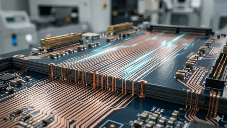
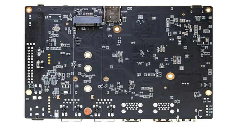
Precision RF Impedance Testing on Rogers RO4350B PCB Prototype
- Rapid Prototyping Delays & Schedule Risk Standard PCB vendors often require 10–14 days for high‑frequency materials due to substrate supply lag and complex lamination cycles. Hongda Circuit eliminates this by maintaining in‑house inventory of raw Rogers laminates and implementing a dedicated 24‑48H rapid turn line.
- Excessive NRE & Small‑Batch Unit Costs Traditional suppliers impose heavy non‑recurring engineering (NRE) tooling charges on small prototype batches. By leveraging automated panelization and flexible tooling, we deliver cost‑optimized Rogers 4350 PCB quotes without compromising material authenticity.
- Strict RF Impedance & Tolerances (±5%) At frequencies above 5 GHz, trace width variations of just a few microns trigger impedance drift and signal degradation. Hongda Circuit applies LDI patterning and automated optical measurement (AOI) to guarantee strict ±5% impedance tolerance across every prototype batch.
- DFM & Hybrid Stackup Misalignment Mismatching the Coefficient of Thermal Expansion (CTE) in hybrid Rogers + FR‑4 stackups often leads to board warping or hole wall cracking. Our prefabrication DFM analysis simulates thermal expansion to guarantee 100% structural integrity during reflow.
2. Specialized Rogers PCB Prototype Fabrication Capabilities
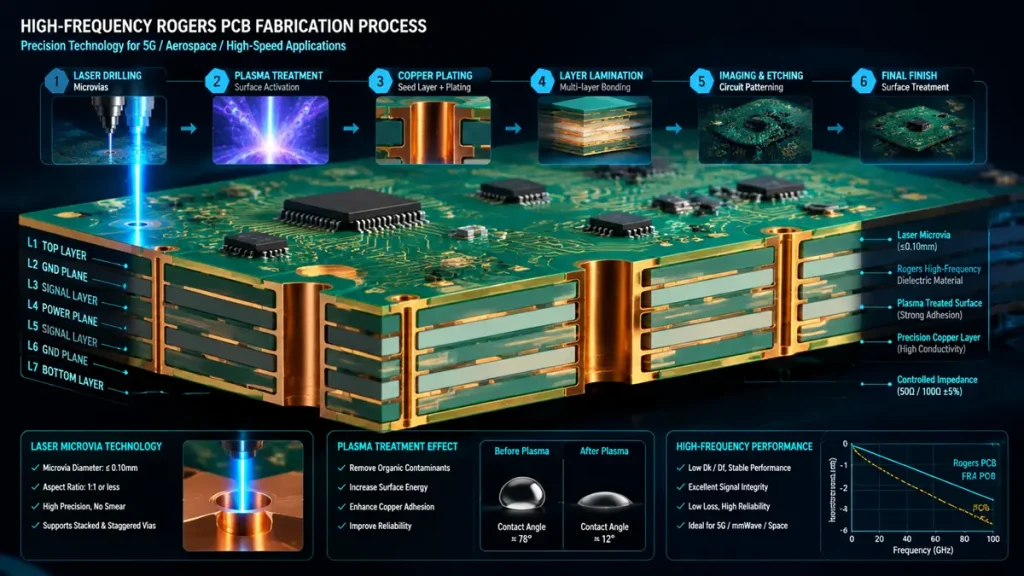
High-Frequency Rogers PCB Fabrication Process & Layer Stackup Diagram
Fabricating prototype high‑frequency boards requires dedicated process controls far superior to standard FR‑4 processing lines. Below is a detailed matrix of Hongda Circuit’s technical capabilities for Rogers substrate fabrication:
| Process / Parameter | Standard Prototype Spec | Advanced RF Capability (2026 Ready) |
|---|---|---|
| Supported Rogers Materials | RO4350B, RO4003C, RO3003 | RT/duroid 5880/6002, RO4835, RO3035, TMM Series |
| Impedance Control Tolerance | ±7% or ±10% | ±5% Strict Tolerance (TDR Verified to 40+ GHz) |
| Surface Finish | uin) | Hard Gold (30 pin), Immersion Silver, ENEPIG |
| Copper Foil Options | Standard Electrodeposited (ED) | Reverse Treated Foll (LoPro), Ultra‑Low Roughness (<0.5 um) |
| Hybrid Stackup Capability | 2‑Layer Pure Rogers | Up to 24‑Layer Hybrid Stackups (Rogers + High‑Tg FR‑4) |
Shenzhen Hongda Circuit Technology Co., Ltd. | Rapid Rogers PCB Prototyping
3. Fast‑Track Lead Times & Service Tiers
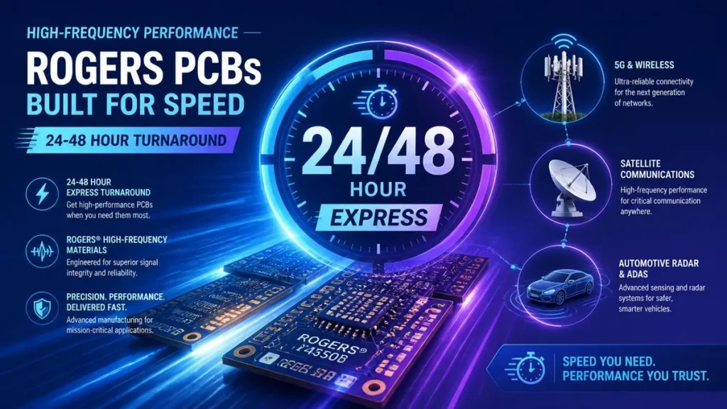
Rapid 24-48 Hour Rogers PCB Prototype Express Service
To support urgent engineering qualification deadlines, Hongda Circuit offers structured prototyping tiers backed by our No‑MOQ (Minimum Order Quantity) guarantee:
| Service Tier | Layer Count | Target Turnaround Time | Recommended Application |
|---|---|---|---|
| Super Express | 2‑Layer (RO4350B/ RO4003C) | 24 Hours | Urgent RF Antenna / Coupler Proof‑of‑ Concept |
| Express Turn | 4‑Layer Hybrid Stackup | 48 Hours | 5G Transceiver & loT Module Verification |
| Standard Quick‑Turn | 6‑10 Layer Multilayer RF | 5‑7 Working Days | Automotive 77GHz Radar & AI Server Backplanes |
| PTFE Special Turn | RT/duroid Series (PTFE) | 7‑10 Working Days | Aerospace Radar & Satellite Payload Systems |
4. Seamless Quote‑to‑Production Workflow
Getting an instant and accurate Rogers 4350 PCB quote is streamlined through our 4‑step digital engineering portal:
- Gerber & Stackup Upload: Submit your Gerber RS‑274X / ODB++ files along with dielectric thickness and copper weight specifications via sales@pcbkr.com.
- Automated 30‑Minute DFM Audit: Our CAM engineers evaluate line/space geometry, drill aspect ratios, and CTE compatibility. You receive an automated DFM report highlighting potential fabrication risks within 30 minutes.
- 3D Impedance Simulation: Using Polar SI9000 field solvers, we verify your target trace impedance against actual substrate lot parameters and output a precise stackup recommendation.
- Instant Direct‑Factory Quotation: Receive transparent pricing with line‑item breakdowns for material, NRE, and express shipping options. No hidden fees or middleman markups.
Ready to Accelerate Your Rogers PCB Prototype?
Upload your Gerber files now for a complimentary DFM audit, 3D impedance validation report, and an instant, direct‑factory quotation within 30 minutes.
Shenzhen Hongda Circuit Technology Co., Ltd.
Room 1608‑1610, Baoyunda Logistics Center, Baoan, Shenzhen, China
Website: www.pcbkr.com
📧 Email: sales@pcbkr.com
Phone: +86 0755 23720053
FAQ
How long does it take to receive a formal quotation and DFM report after submitting Gerber files?
Once you submit your Gerber RS-274X or ODB++ files along with your stackup requirements, our CAM engineering team performs an automated DFM audit within 30 minutes. You will receive an automated DFM report highlighting line/space geometry, drill aspect ratios, and thermal expansion (CTE) compatibility, alongside a transparent, direct-factory quotation covering materials, NRE, and express shipping.
How does Hongda Circuit guarantee impedance precision and signal integrity for RF boards above 5 GHz?
At frequencies above 5 GHz, minute trace width variations cause impedance drift. Hongda Circuit applies Laser Direct Imaging (LDI) patterning and Automated Optical Inspection (AOI) to guarantee a strict ±5% impedance tolerance across every prototype batch. Furthermore, we utilize Polar SI9000 field solvers for 3D impedance simulation and verify performance with TDR testing up to 40+ GHz.
What are Hongda Circuit’s layer count capabilities and turnaround times for hybrid Rogers stackups?
To balance RF performance with cost, we support hybrid stackups up to 24 layers combining Rogers substrates with high-Tg FR-4. For 4-layer hybrid stackups, we offer a 48-Hour Express Turn to help engineering teams rapidly verify 5G transceivers and IoT modules. For standard 6–10 layer multilayer RF designs, our lead time is 5–7 working days.
Is there a Minimum Order Quantity (MOQ) or heavy NRE tooling fee for low-volume Rogers prototyping?
We operate under a strict No-MOQ policy (1-piece minimum). By leveraging automated panelization and flexible tooling, Hongda Circuit significantly reduces non-recurring engineering (NRE) costs for small prototype batches without compromising on genuine Rogers raw material quality.
What advanced manufacturing capabilities does Hongda Circuit offer for PTFE/duroid substrates?
For complex PTFE-based laminates like RT/duroid 5880/6002, RO4835, and the TMM series, we employ Plasma Surface Activation for hole desmear and preparation to guarantee barrel plating integrity. Additionally, our 2026-ready capabilities include 0.31 mil (8 µm) mSAP fine traces, 50 µm laser microvias (Any-Layer HDI), and ultra-low roughness copper foil (<0.5 µm LoPro®).
About Author
David Chen https://www.linkedin.com/in/pcbcoming
David Chen boasts an extensive professional background in PCBA manufacturing, PCBA testing, and PCBA optimization, with specialized expertise in high-precision PCBA fault analysis and rigorous PCBA reliability testing. The author has worked with high-layer-count server PCB fabrication, ultra-low-loss backplane stackups, and thermo-mechanical reliability optimization for AI infrastructure projects involving 112G and 224G PAM4 architectures. Skilled in complex circuit design and cutting-edge advanced PCB manufacturing processes, he delivers solutions that elevate product durability and performance across industrial applications. His technical articles focusing on PCBA manufacturing workflows and testing methodologies are widely cited by industry peers, research institutions, and technical platforms, solidifying his reputation as a recognized technical authority in the global circuit board manufacturing sector.