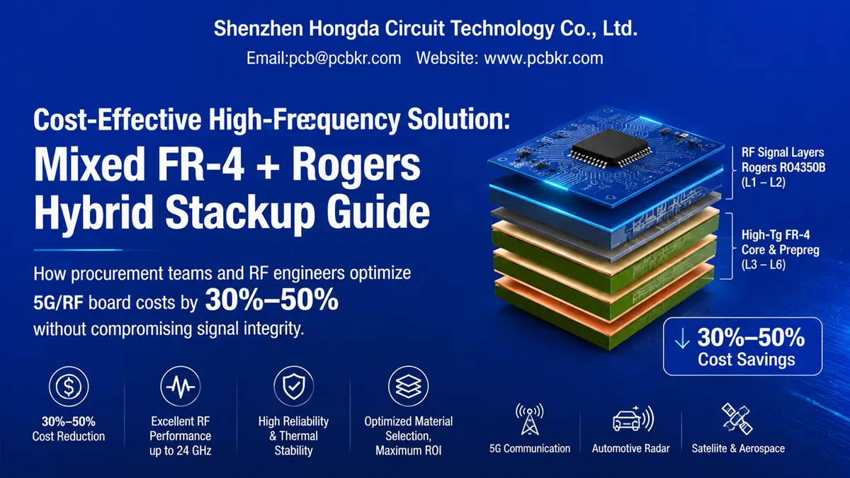
Cost‑Effective High‑Frequency Solution: Mixed FR‑4 + Rogers Hybrid Stackup Guide
How procurement teams and RF engineers optimize 5G/RF board costs by 30%–50% without compromising signal integrity.
The Cost vs. Physics Dilemma in Multilayer RF PCBs
As highlighted in our foundational pillar guide, “The Definitive Guide to Rogers PCB: Material Properties, Manufacturing & RF Applications,” high‑frequency designs above 5 GHz transition from a pure cost decision into an unyielding physics problem. When engineers specify premium laminates like Rogers RO4350B or RO4003C for multilayer boards, procurement teams frequently encounter severe sticker shock—unit substrate costs can be 3× to 5× higher than standard glass‑reinforced epoxy (FR‑4).
However, a closer audit of most 6‑layer, 8‑layer, or 12‑layer RF designs reveals an essential engineering truth: less than 20% to 30% of the total trace routing actually carries sensitive millimeter‑wave or RF signals. Routing non‑critical power planes, low‑speed digital control lines, and ground return layers on expensive high‑frequency laminates represents a major cost inefficiency.
The solution? Mixed FR‑4 + Rogers hybrid stackups (also known as hybrid laminates). By selectively placing high‑frequency Rogers laminates only on top/bottom signal layers where RF performance is required, and utilizing standard high‑Tg FR‑4 for inner power and digital layers, engineering teams achieve the precise signal integrity required for 5G, automotive radar, and satellite communications—while procurement slashes raw material expenditures by 30% to 50%.
Key Procurement Takeaway
If you are searching for a way to get a rogers 4350 pcb cheap without sacrificing RF pass‑band performance or long‑term thermal reliability, a mixed fr‑4 + rogers pcb hybrid stackup is the industry’s gold standard strategy.
Engineering Deep‑Dive: Technical Challenges of Hybrid Lamination
While hybrid stackups offer massive commercial benefits, joining fundamentally dissimilar substrate materials inside a single PCB panel introduces severe manufacturing challenges. A reliable high‑frequency PCB manufacturer must overcome three primary physics‑driven hurdles during lamination:
- Coefficient of Thermal Expansion (CTE) Mismatch Standard FR‑4 materials feature an out‑of‑plane (Z‑axis) CTE of 50 to 70 ppm/°C, whereas thermoset hydrocarbon ceramics like Rogers RO4350B exhibit a tightly controlled Z‑axis CTE of 32 ppm/°C (closely matched to copper at 17 ppm/°C). During thermal reflow cycles (up to 260°C for lead‑free assembly), unequal expansion rates across heterogeneous material layers can generate severe internal shear stress, leading to plated‑through‑hole (PTH) barrel cracking, via pad tearing, or micro‑delamination.
Shenzhen Hongda Circuit Technology Co., Ltd. | Technical Blog Page 1 of 3
- Resin Cure Temperature & Lamination Pressure Matching Rogers hydrocarbon ceramic substrates (RO4000 series) and epoxy‑based FR‑4 prepregs react differently under heat and pressure:
- Hydrocarbon Thermoset Prepregs (e.g., Rogers RO4450F / RO4450T): Require precise, higher curing temperatures (~175°C to 200°C) and specific pressure ramp profiles to flow smoothly without resin starvation.
- High‑Tg FR‑4 Prepregs: Require matched glass transition \((Tg>170^{\circ} C)\) and compatible resin flow windows to prevent over‑curing or uneven thickness across the panel.
- Symmetrical Stackup Design & Warpage Control Heterogeneous material asymmetry is the leading cause of board bow and twist. To ensure mechanical flatness post‑lamination, PCB designers and manufacturers must enforce symmetrical layer distribution (e.g., matching dielectric thicknesses and copper coverage balance across the center neutral axis).
Commercial ROI Analysis: Pure Rogers vs. Hybrid FR‑4 + Rogers Stackup
To illustrate the financial impact, let us examine a real‑world 6‑layer high‑frequency board deployed in a 24 GHz smart radar transceiver module.
| Parameter / Feature | Pure Rogers Stackup (All 6 Layers) | Mixed FR‑4 + Rogers Hybrid Stackup | Procurement & Technical Impact |
|---|---|---|---|
| Substrate Architecture | 6 Layers of Rogers RO4350B | L1‑L2: Rogers RO4350B (0.254mm) L3‑L6: High‑Tg FR‑4 Core & Prepreg | Selective RF material placement on top surface layer |
| Cost Laminate Raw Material | 100% Baseline ($$$) | 45% – 55% Baseline ($) | 45% to 55% direct material savings |
| Reduction Total PCB Unit Price | 0% Baseline | 35% – 48% Total Savings | Delivers rogers 4350 pcb cheap unit cost |
| 24 GHz Insertion Loss | ~0.045 dB/mm | ~0.045 dB/mm (RF traces on L1) | Identical high‑frequency performance |
| (50 Ω) Impedance Tolerance | ± 5% | ± 5% (LDI imaging + L1‑ L2 control) | Zero compromise on RF signal integrity |
| Reliability Reflow Thermal | High (5x Reflow Pass) | High (Passed 6x Lead‑ Free Reflow) | High‑Tg FR‑4 core prevents Z‑axis CTE fatigue |
Design & Procurement Guidelines for Hybrid Stackups
When procuring or designing a mixed fr‑4 + rogers pcb, incorporating the following Design for Manufacturability (DFM) rules ensures high fabrication yield and zero field failures:
- Specify Rogers RO4000 Series for Hybrid Builds: Thermoset hydrocarbon materials like RO4350B and RO4003C process similarly to standard FR‑4, making them ideal for hybrid bonding. PTFE‑based materials (like RT/duroid 5880) require specialized sodium/plasma surface activation and are significantly harder to bond reliably with FR‑4.
Shenzhen Hongda Circuit Technology Co., Ltd. | Technical Blog Page 2 of 3
- Use Specialized Bonding Prepreg: Always bond Rogers RO4000 cores to FR‑4 inner layers using compatible high‑performance prepreg, such as Rogers RO4450F / RO4450T prepreg or high‑Tg FR‑4 prepreg with matching rheological flow characteristics.
- Enforce Symmetrical Dielectric Construction: Balance the total thickness and copper weight across the core center plane to prevent panel warpage during automated SMT component placement.
- Optimize Ground Return & Via Transitions: Ensure ground vias surround signal microvia transitions between L1 (Rogers) and L2 (FR‑4 ground plane) to maintain continuous 50 Ω coplanar wave guide impedance.
Why Partner with Shenzhen Hongda Circuit Technology ?
Executing a seamless hybrid stackup requires advanced press capability and precise lamination recipe control. Shenzhen Hongda Circuit Technology Co., Ltd. (www.pcbkr.com) is a premier specialist in high‑frequency hybrid PCB fabrication:
- State‑of‑the‑Art Lamination Infrastructure: We utilize multi‑stage LAUFFER lamination presses with computerized thermal ramp profiles designed specifically for high‑Tg FR‑4 and Rogers hydrocarbon ceramic cocure recipes.
- Advanced Fineline & HDI Capability: Equipped with SCREEN Ledia LDI exposure and Mitsubishi \(UV/CO\) hybrid laser drilling, we support mSAP traces down to 8 μm line/space and microvia diameter down to 50 μm.
- Full Lot Traceability & Quality Certification: ISO 9001, AS9100D, IATF 16949, and IPC Class 3/3A certified. Every shipment includes lot‑specific certificates of conformance, Dk/Df material certificates, and TDR impedance reports.
- Procurement‑Friendly Agile Service: No MOQ requirements for rapid prototypes (5–7 day lead times) and 24hour rapid DFM stackup consultation.
Ready to Optimize Your High‑Frequency Board Costs?
Get a complimentary 24‑hour DFM evaluation, hybrid stackup impedance simulation, and quotation to see how much you can save on your next mixed fr‑4 + rogers pcb project.
Email: sales@pcbkr.com
Phone: +86 0755 23720053
Website: www.pcbkr.com
Company: Shenzhen Hongda Circuit Technology Co., Ltd.
Address: Room 1608‑1610, R&D Building, Baoyunda Logistics Center, Baoan, Shenzhen, China
FAQ
How much cost savings can we expect by switching from a pure Rogers RO4350B stackup to a Rogers + FR4 mixed dielectric hybrid PCB?
By adopting a Rogers RO4350B + FR4 hybrid stackup (where RO4350B is selectively used on top/bottom RF signal layers and High-Tg FR-4 is used for inner/power layers), procurement teams typically achieve a 45% to 55% reduction in raw material substrate costs and a 35% to 48% overall reduction in the total PCB unit price, while maintaining identical 50 Ω impedance control and RF insertion loss.
Will combining Rogers RO4350B with High-Tg FR4 affect signal integrity or thermal reliability during reflow soldering?
No, provided the stackup follows strict DFM rules. Because RO4350B is a thermoset hydrocarbon ceramic material, its processing temperature and Z-axis CTE (32 ppm/°C) are well-aligned with high-performance copper and High-Tg FR-4 (Tg > 170°C). When properly bonded using compatible prepregs (such as Rogers RO4450F/T), the hybrid board successfully passes up to 6x lead-free reflow cycles (260°C) without plated-through-hole (PTH) cracking or micro-delamination.
What prepreg and material combination should be specified when procuring Rogers RO4350B + FR4 hybrid PCBs?
It is recommended to specify Rogers RO4000 series cores (e.g., RO4350B) for the RF layers, combined with High-Tg FR-4 cores (Tg > 170°C) for internal digital/power routing. For bonding, use specialized prepregs such as Rogers RO4450F or RO4450T, or high-Tg FR-4 prepregs with matched resin flow windows to prevent over-curing, resin starvation, or asymmetrical warpage.
How do we evaluate if a PCB manufacturer has qualified manufacturing capabilities for Rogers RO4350B + FR4 mixed dielectric stackups?
When auditing suppliers, ensure they possess:
1. Advanced Lamination Equipment: Multi-stage presses (e.g., LAUFFER) capable of precise multi-ramp thermal and pressure profiles.
2. High-Precision Drilling & Imaging: Laser drilling ($UV/CO_2$) for microvias and Direct Imaging (LDI) for tight trace/space tolerance control.
3. Quality Certifications & Testing Reports: ISO 9001, IATF 16949, or AS9100D certifications, along with lot-specific TDR impedance reports and Dk/Df certificates of conformance with every batch.
What is the typical lead time and Minimum Order Quantity (MOQ) for Rogers RO4350B + FR4 hybrid PCB prototypes?
Leading high-frequency PCB manufacturers (such as Shenzhen Hongda Circuit Technology / Hongda Circuit) offer No MOQ requirements for rapid prototyping, with standard prototype lead times ranging between 5 to 7 business days. They also provide 24-hour rapid DFM evaluations and TDR stackup simulations prior to fabrication to eliminate design risks early.
About Author
David Chen https://www.linkedin.com/in/pcbcoming
David Chen boasts an extensive professional background in PCBA manufacturing, PCBA testing, and PCBA optimization, with specialized expertise in high-precision PCBA fault analysis and rigorous PCBA reliability testing. The author has worked with high-layer-count server PCB fabrication, ultra-low-loss backplane stackups, and thermo-mechanical reliability optimization for AI infrastructure projects involving 112G and 224G PAM4 architectures. Skilled in complex circuit design and cutting-edge advanced PCB manufacturing processes, he delivers solutions that elevate product durability and performance across industrial applications. His technical articles focusing on PCBA manufacturing workflows and testing methodologies are widely cited by industry peers, research institutions, and technical platforms, solidifying his reputation as a recognized technical authority in the global circuit board manufacturing sector.