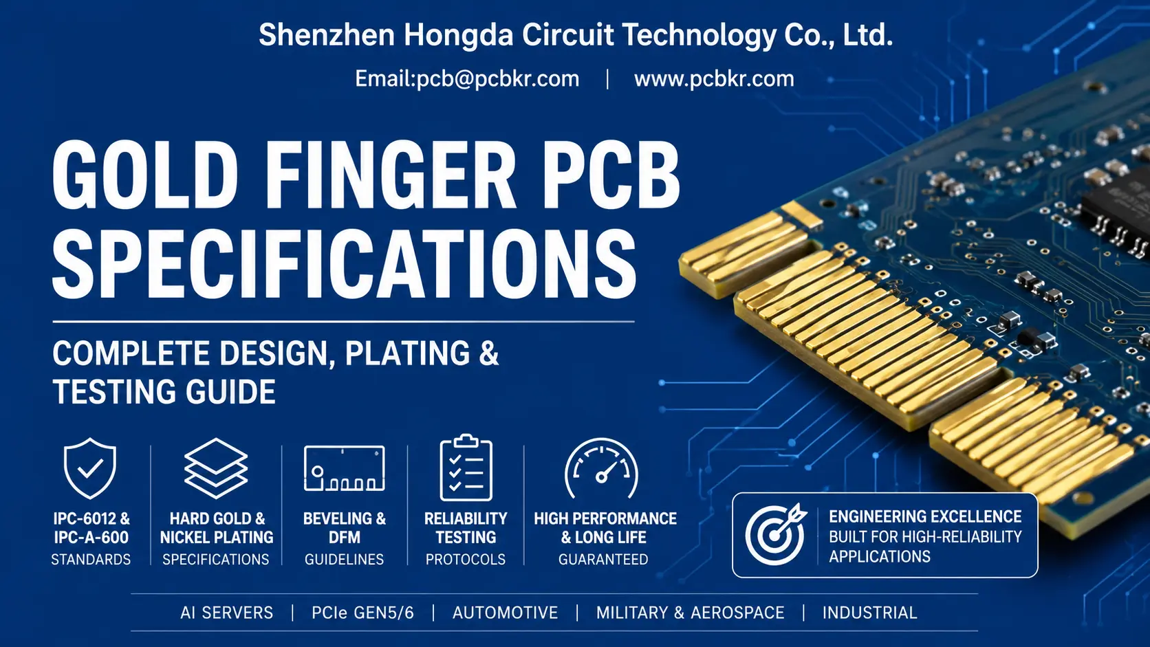
Gold Finger PCB Specifications & IPC Standards: Complete Design, Plating & Testing Guide
Gold Finger PCB Specifications: This guide covers full IPC standards, plating stackup, mechanical design, reliability testing and supplier selection for gold finger edge connector PCBs, including Class 2 / Class 3 performance difference, hard gold vs ENIG comparison, as well as high-reliability application requirements for PCIe, automotive and military scenarios.
What Are Gold Finger PCBs and Why Do Edge Connector Specifications Matter?
A gold finger PCB—also referred to as a PCB edge connector or card-edge contact board—is a printed circuit board with hard-gold-plated contact pads along one edge that mate with a card-edge socket. These plated edge contacts carry power, ground, and high-speed signals between boards in systems ranging from PCIe expansion cards and DDR memory modules to blade servers and industrial backplanes.
In 2026, as AI servers push 224G PAM4 signaling and automotive domain controllers demand zero-defect reliability, the margin for error in gold finger plating specifications has effectively vanished. A single contact resistance spike caused by porous gold, insufficient nickel underplate, or improper beveling geometry can trigger signal integrity collapse or field failure. Procurement engineers and hardware designers who treat edge connector plating as a commodity specification rather than a reliability-critical process often discover—too late—that their 30 µin gold thickness was calculated for 50 insertion cycles in a climate-controlled lab, not 1,000+ hot-swaps in a dusty data center.
At Shenzhen Hongda Circuit Technology Co., Ltd., we have observed that roughly 60% of gold finger field failures traced back to the fabrication stage originate from three root causes: sub-threshold nickel barrier thickness, uncontrolled cobalt content in the hard gold matrix, and bevel angles that generate fretting debris under vibration. This guide consolidates the IPC-6012F, IPC-A-600, and IPC-TM-650 frameworks with our in-house production data to give you specification limits you can actually build against.
Quick-Reference: Gold Finger PCB Core Specifications
| Parameter | IPC-6012 Class 2 (General Electronics) | IPC-6012 Class 3 / 3A (High-Reliability) | Typical Application |
|---|---|---|---|
| Hard Gold Thickness | 15–30 µin (0.38–0.76 µm) | 30–50+ µin (0.76–1.27+ µm) | PCIe Gen5/6, DIMM, VPX |
| Nickel Underplate | 100–150 µin (2.54–3.81 µm) | 150–300 µin (3.81–7.62 µm) | Military, Medical, Automotive |
| Knoop Hardness | 130–200 HK | 130–200 HK | Wear resistance vs. ductility |
| Bevel Angle | 20°–30° | 30°–45° | Insertion force & edge chipping |
| Insertion Cycles (30 µin Au) | 200–500 | 500–1,000+ | Telecom vs. Aerospace |
IPC-6012 & IPC-A-600 Standards for Gold Finger PCBs: Class 2 vs. Class 3 Decoded
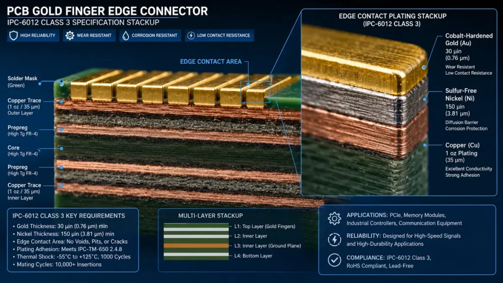
IPC-6012 Class 3 Gold Finger PCB Plating Stackup Diagram
IPC-6012F: The Performance Specification Baseline
IPC-6012F—the current revision of the Qualification and Performance Specification for Rigid Printed Boards—defines the minimum acceptability criteria for gold finger edge connector plating based on end-use environment. The distinction between Class 2 (dedicated service electronics) and Class 3 (high-performance/high-reliability) is not merely a marketing label; it directly dictates plating thickness, porosity limits, and thermal stress testing protocols.
For Class 3 gold finger PCBs, IPC-6012F mandates a minimum hard gold thickness of 30 µin over a nickel underplate no thinner than 150 µin. Class 2 permits a reduction to 15 µin gold in non-critical consumer applications, but experienced procurement teams rarely spec below 30 µin for anything carrying digital signals above 1 GHz—skin effect losses and surface oxidation risks escalate quickly below that threshold.
At Shenzhen Hongda Circuit, our production line defaults to IPC-6012 Class 3 process control even for Class 2 quotes unless explicitly waived by the customer. Our rationale: the cost delta between 20 µin and 30 µin hard gold is negligible compared to the cost of a field failure in a 40-layer AI server backplane.
IPC-A-600: Visual & Microsection Acceptance Criteria
While IPC-6012F defines performance, IPC-A-600 defines acceptability. For gold fingers, the critical defect categories include:
- Porosity (Porosity Test per IPC-TM-650 2.3.24): Class 3 requires zero porosity in the contact zone when tested with nitric acid vapor. Any pore penetrating to the nickel layer constitutes a reject.
- Pits & Voids: Surface pits deeper than 10% of the gold thickness or exceeding 0.08 mm in diameter are non-conforming for Class 3.
- Scratch Exposure: Scratches revealing nickel or copper beneath the gold layer are unacceptable on any edge connector contact surface.
- Edge Chipping: Post-beveling, chipping that reduces the effective contact length by more than 5% is grounds for rejection.
Our AI-enhanced AOI system at Hongda Circuit performs 100% surface inspection of gold finger zones at >99.9% defect detection rates, with predictive reliability analysis flagging panels that may pass visual criteria but exhibit micro-porosity risk under thermal cycling.
Structured Comparison: IPC Class 2 vs. Class 3 Gold Finger Requirements
| Criterion | IPC-6012 Class 2 | IPC-6012 Class 3 / 3A | Testing Method |
|---|---|---|---|
| Gold Thickness (min) | 15 µin (0.38 µm) | 30 µin (0.76 µm) | XRF or Microsection |
| Nickel Thickness (min) | 100 µin (2.54 µm) | 150 µin (3.81 µm) | Microsection |
| Porosity (contact area) | ≤5 pores/cm² | 0 pores in contact zone | IPC-TM-650 2.3.24 |
| Thermal Stress | 3 cycles @ 288°C | 6 cycles @ 288°C | IPC-TM-650 2.6.8 |
| Solderability (if mixed finish) | N/A | Must not degrade Au/Ni | IPC-TM-650 2.4.14 |
Gold Finger Plating Layer & Material Specifications: Hard Gold vs. ENIG
Hard Gold (Electrolytic Gold) Composition and Thickness Optimization
Hard gold plating for PCB edge connectors is an electrolytic process depositing a cobalt-hardened gold matrix (typically 0.1–0.3% Co by weight) over an electroplated nickel underlayer. The cobalt interstitial structure raises Knoop hardness to 130–200 HK, transforming the deposit from a soft, wear-prone film into a tribologically stable contact surface.
The standard gold thickness for gold fingers spans 15 µin to 50 µin (0.38 µm–1.27 µm), with the selection driven by insertion cycle requirements:
- 15–20 µin: Suitable for <100 insertion cycles; consumer-grade peripherals with static installation.
- 30 µin: The industry sweet spot for 500–1,000 cycles; standard for PCIe cards, server DIMMs, and industrial I/O modules.
- 50 µin+: Required for 1,000–10,000+ cycles; high-reliability military backplanes, test fixtures, and hot-swappable storage arrays.
At Shenzhen Hongda Circuit, our pulse-reverse electroplating lines achieve ±8% thickness uniformity across the full panel edge, even on 21″ × 24″ backplanes. Unlike conventional DC plating, pulse-reverse current distribution minimizes edge-thickness buildup and ensures the nickel diffusion barrier maintains consistent thickness beneath every contact pad.
Nickel Underplate: The Diffusion Barrier That Determines Long-Term Reliability
Nickel is not merely a substrate for gold; it is the diffusion barrier preventing copper migration into the gold layer and gold diffusion into the copper trace. Without adequate nickel thickness, two failure modes emerge:
- Copper Exudation: Copper atoms diffuse through thin gold grain boundaries, oxidize at the surface, and elevate contact resistance beyond the 20 mΩ threshold.
- Kirkendall Voiding: Differential diffusion rates between copper and gold create voids at the interface, mechanically weakening the deposit.
Standard nickel thickness for gold fingers ranges from 100 µin to 300 µin (2.54 µm–7.62 µm). For high-temperature applications—automotive under-hood modules or aerospace avionics—we recommend 200 µin minimum. Our electroplating chemistry at Hongda Circuit maintains sulfur-free nickel deposits with <100 ppm codeposited organic impurities, eliminating the sulfur-induced corrosion risk that has plagued some Asian suppliers in recent automotive recalls.
ENIG vs. Hard Gold: Why Immersion Gold Fails at Edge Connectors
A recurring question from procurement teams is whether ENIG (Electroless Nickel Immersion Gold) can substitute for hard gold on edge connectors. The short answer: only if the design will never see mechanical wear.
ENIG deposits a soft gold layer (typically 3–6 µin, 0.08–0.15 µm) with Knoop hardness <90 HK. Under insertion forces exceeding 1 N per contact, this layer abrades within 10–20 cycles, exposing the nickel beneath. Nickel oxide formation then drives contact resistance above 100 mΩ, causing signal dropouts. ENIG remains excellent for BGA pads and SMT lands, but for any plated edge connector subject to insertion cycles, electrolytic hard gold is non-negotiable.
Mechanical & Electrical Performance Requirements for Gold Finger Edge Connectors
Wear Resistance and Insertion Cycle Life by Gold Thickness
The relationship between gold finger thickness and insertion life is non-linear due to work-hardening effects. Our in-house insertion/extraction testing—conducted on a custom 50-position actuator simulating PCIe Gen5 mating forces—yields the following empirical data:
| Hard Gold Thickness | Mean Cycles to 50% Au Loss | Contact Resistance Delta @ EOL | Best-Fit Application |
|---|---|---|---|
| 15 µin | 150–250 cycles | +15 mΩ | Low-cost IoT dongles |
| 30 µin | 800–1,200 cycles | +8 mΩ | Server DIMMs, GPU cards |
| 50 µin | 3,000–5,000 cycles | +3 mΩ | Telecom backplanes |
| 80 µin (selective) | 10,000+ cycles | <+2 mΩ | Test interface boards |
Test conditions: 1.5 N/contact, 1 mm/s insertion speed, 25°C, 45% RH, per EIA-364-09.
Contact Resistance Standards for High-Speed Gold Finger Interfaces
Contact resistance is the silent killer of high-speed gold finger designs. While DC specifications often cite <20 mΩ as acceptable, 224G PAM4 signaling demands stable resistance across the full operating temperature range (-40°C to +125°C for automotive Grade 1).
At Shenzhen Hongda Circuit, we specify:
- Initial contact resistance: <10 mΩ (measured four-wire Kelvin method)
- Post-thermal aging (1,000 hr @ 125°C): <15 mΩ
- Post-vibration (MIL-STD-202G, Method 204D): <12 mΩ
These limits are validated on every production lot using our flying probe electrical test systems with dedicated gold finger contact resistance test coupons.
Beveling and Chamfering Geometry: The 30-Degree Rule
PCB gold finger beveling—the angled cut at the insertion edge—serves two functions: reducing insertion force and preventing gold layer peeling. Standard bevel angles are:
- 20°: Aggressive insertion, minimum PCB real estate; risk of edge burrs if plating is brittle.
- 30°: The universal compromise; compatible with 0.8 mm–2.0 mm board thickness; used in 90% of PCIe and VPX designs.
- 45°: Gentle ramp for thick boards (>3.0 mm) or high-pin-count backplanes where insertion force must be distributed.
Our CNC beveling stations at Hongda Circuit maintain ±0.5° angular tolerance and 0.05 mm edge straightness, with post-bevel ionic cleanliness verification to ensure no conductive debris remains in the contact zone.
Gold Finger PCB Qualification & Reliability Testing Protocols
Salt Spray Corrosion Testing (ASTM B117)
For marine, automotive, and industrial deployments, ASTM B117 salt fog testing is the definitive validation of gold finger porosity and nickel barrier integrity. Our standard protocol:
- Duration: 48 hours (automotive), 96 hours (marine/military)
- Conditions: 5% NaCl, 35°C, pH 6.5–7.2
- Acceptance: No visible corrosion products on contact surfaces; no nickel underplate exposure; contact resistance delta <5 mΩ post-test.
Hongda Circuit maintains an in-house salt spray chamber with continuous monitoring, eliminating third-party lab delays for urgent qualification builds.
Adhesion Testing (IPC-TM-650 2.4.1 Tape Test)
The 3M tape adhesion test remains the simplest and most effective validation of gold-to-nickel cohesion. After scoring the gold surface in a 1 mm grid pattern, high-tack tape is applied and removed rapidly. Any gold flaking onto the tape constitutes a process failure—typically indicating organic contamination at the nickel-gold interface or excessive cobalt content embrittling the deposit.
RoHS 3.0 & REACH Compliance for Gold Finger Materials
Modern procurement mandates extend beyond performance to environmental compliance. Our hard gold plating chemistry is certified free of lead, cadmium, hexavalent chromium, and restricted phthalates under EU RoHS Directive (EU) 2015/863 (RoHS 3.0) and REACH SVHC thresholds. Full material declaration (FMD) and lot-level test reports are available for every production run.
Gold Finger PCB Design for Manufacturability (DFM) Guidelines
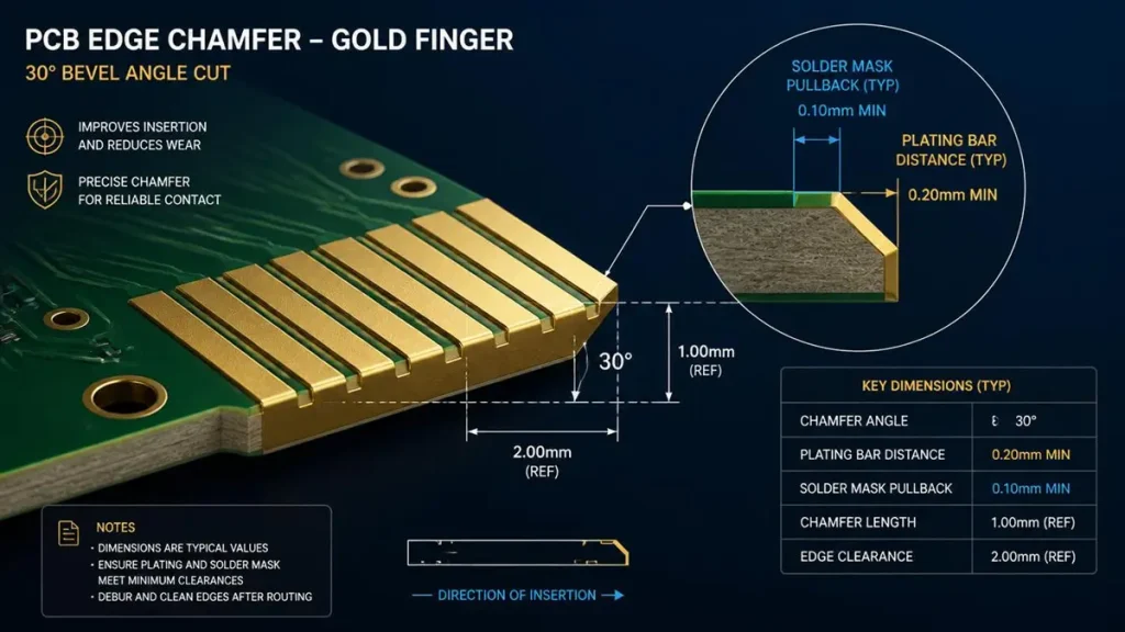
PCB Gold Finger Edge Chamfer Design Rules (30° Bevel)
Plating Bar Design and Edge Distance
Hard gold electroplating requires a plating bar (thieving busbar) to distribute current to the edge connector pads. Critical DFM rules:
- Plating bar width: ≥1.0 mm to prevent current crowding and thickness variation.
- Distance to rout edge: Maintain ≥0.5 mm clearance between the outermost gold finger pad and the final board edge to prevent nickel-gold creep onto the sidewall.
- Tab routing: Use mouse-bite depaneling for gold finger boards; V-scoring can fracture the beveled edge.
Solder Mask Clearance Around Gold Fingers
Solder mask clearance for PCB edge connectors must expose the full contact pad while preventing mask bleed onto the mating surface. Our LDI imaging systems at Hongda Circuit achieve ±10 µm solder mask registration, ensuring a 0.1 mm minimum mask pullback from the gold finger edge without exposing adjacent circuitry.
Inner-Layer Copper Peel Strength and Delamination Prevention
Repeated insertion stress can propagate microcracks from the gold finger surface into the board interior. For high-insertion-cycle designs, we recommend:
- Inner-layer copper peel strength: ≥1.05 N/mm per IPC-TM-650 2.4.8
- Z-axis CTE matching: Use high-Tg (≥170°C) laminate to reduce thermal expansion mismatch between the FR-4 core and the copper/nickel/gold stackup during reflow.
- Edge reinforcement: For boards >3.2 mm thick, consider adding a 0.5 mm unfilled fiberglass edge band to absorb insertion shock.
Frequently Asked Questions: Gold Finger PCB Procurement & Supplier Selection
What is the standard gold thickness for PCIe gold fingers, and does it differ between Gen4 and Gen5?
For PCIe gold finger specifications, the PCI-SIG mechanical specification calls for a minimum of 0.8 µm (31 µin) hard gold over 3.8 µm nickel for both Gen4 and Gen5 add-in cards. However, Gen5’s higher signal integrity margin and tighter insertion force tolerances make 30–50 µin the de facto procurement standard. At Shenzhen Hongda Circuit, we default to 40 µin for all PCIe server-grade builds to account for connector vendor tolerance stack-up.
Can ENIG be used for gold fingers if cost is a primary concern?
No. ENIG for PCB edge connectors is a false economy. While ENIG offers excellent solderability for SMT pads, its immersion gold layer (3–6 µin) is too thin and soft to survive even 50 mechanical insertion cycles. For cost-sensitive applications with low cycle counts, specify 15 µin electrolytic hard gold rather than ENIG. The plating cost difference is typically <$0.50 per board at volume, while the reliability improvement is orders of magnitude.
How do I audit a PCB supplier’s gold finger plating process during a factory visit?
Procurement engineers should verify four critical process controls on-site:
1. Chemistry bath analysis logs: Cobalt content in the hard gold bath should be 0.1–0.3% by weight; nickel bath pH should be 3.8–4.2.
2. Thickness verification: Ask to see XRF calibration certificates and witness a live measurement on a production panel—uniformity should be ±10% edge-to-edge.
3.Beveling QC: Check CNC bevel angle gauges for 30° ±1° calibration and inspect edge quality under 10× magnification.
4.Test coupon archive: A qualified supplier retains microsection photos and contact resistance data for every lot for a minimum of 5 years.
What IPC class applies to military and automotive gold finger PCBs, and is Class 3 always sufficient?
IPC-6012 Class 3 is the baseline for military (MIL-PRF-55110) and automotive (IATF 16949) gold finger applications. However, many defense contractors now specify IPC-6012 Class 3A (Aerospace) or augment Class 3 with additional requirements such as 96-hour salt spray, 6× thermal stress, and 100% C-SAM void inspection. For automotive ADAS modules with gold finger backplane interfaces, we recommend Class 3 plus AEC-Q100 stress qualification. Hongda Circuit is certified to both IPC-6012 Class 3 and AS9100D, enabling seamless qualification for dual-use programs.
How can I prevent gold finger oxidation and porosity during long-term storage?
Oxidation of gold fingers is almost always a symptom of underlying porosity, not gold degradation. Prevention strategies include:
1. Packaging: Vacuum-seal with desiccant (silica gel, <10% RH) and anti-tarnish paper (VCI).
2. Storage environment: 15–25°C, <40% RH; avoid sulfur-containing environments (rubber bands, certain cardboard).
3. Shelf life: Hard gold over adequate nickel remains solderable for 12+ months; however, we recommend electrical validation after 6 months for Class 3 applications.
Handling: Mandate nitrile gloves and edge protectors during assembly; skin oils contain chlorides that nucleate corrosion at pore sites.
Hongda Circuit ships all gold finger PCBs in ESD-safe vacuum pouches with humidity indicators and lot-coded storage guidelines.
Why Shenzhen Hongda Circuit Technology Co., Ltd. for Your Gold Finger PCB Requirements
Shenzhen Hongda Circuit Technology Co., Ltd. operates a 2026-spec hard gold plating line dedicated to edge connector applications, with capabilities that include:
- Pulse-reverse electrolytic gold plating: 15–80 µin thickness range, ±8% uniformity on panels up to 24″
- Sulfur-free nickel underplate: 100–300 µin with <100 ppm organic contamination
- CNC precision beveling: 20°–45° angles, ±0.5° tolerance, ionic cleanliness validated
- 100% contact resistance testing: Four-wire Kelvin measurement on every production panel
- Full IPC-6012 Class 3 / AS9100D / IATF 16949 quality system with lot traceability
From AI server PCIe Gen6 accelerator cards to military VPX backplanes, our engineering team provides pre-production DFM review, stackup optimization, and qualification test planning to ensure your gold finger design performs on specification—cycle one and cycle one thousand.
Contact our engineering team for a gold finger PCB specification review or custom plating thickness quotation. Email:pcb@pcbkr.com
About Author
David Chen https://www.linkedin.com/in/pcbcoming
David Chen boasts an extensive professional background in PCBA manufacturing, PCBA testing, and PCBA optimization, with specialized expertise in high-precision PCBA fault analysis and rigorous PCBA reliability testing. The author has worked with high-layer-count server PCB fabrication, ultra-low-loss backplane stackups, and thermo-mechanical reliability optimization for AI infrastructure projects involving 112G and 224G PAM4 architectures. Skilled in complex circuit design and cutting-edge advanced PCB manufacturing processes, he delivers solutions that elevate product durability and performance across industrial applications. His technical articles focusing on PCBA manufacturing workflows and testing methodologies are widely cited by industry peers, research institutions, and technical platforms, solidifying his reputation as a recognized technical authority in the global circuit board manufacturing sector.