Embedded Component PCB Lead Time: Manufacturing & Procurement Guide
Embedded Component PCB lead time is typically 10–20 working days for standard builds and about 15–30+ working days for complex HDI, mSAP, specialty‑material, or multi‑lamination designs. Expedited production may reach 7–10 working days when engineering files, materials, components, capacity, and testing requirements are ready.
For procurement engineers, however, the quoted number is only part of the story. The more important question is whether the supplier can control the critical manufacturing path behind that delivery date.
At Shenzhen Hongda Circuit Technology Co., Ltd., we evaluate embedded PCB lead time from the complete manufacturing route rather than estimating delivery from board quantity alone. This approach considers engineering review, component readiness, cavity processing, embedding, sequential lamination, HDI processing, surface finishing, inspection, yield, and production capacity.
What Is Embedded Component PCB Lead Time?
Embedded Component PCB Lead Time is the elapsed working time from confirmed manufacturing data and order release to completion of PCB fabrication, embedded‑component processing, testing, quality release, and readiness for shipment.
Unlike a conventional PCB schedule, an embedded‑component PCB can combine elements of PCB fabrication, component placement, cavity processing, interconnection, and multilayer lamination within one integrated manufacturing route.
The lead‑time clock should therefore be defined carefully.
A practical definition is:
Embedded Component PCB Lead Time = Engineering Release → Material Readiness → Manufacturing → Embedding → Inspection/Test → Quality Release
The exact starting point should be confirmed with the supplier.
For procurement teams, this distinction matters because a supplier may quote a fabrication time that begins only after all materials and components are available.
PCBWay, for example, explicitly states that its PCBA turn‑time begins after the required parts and manufacturing data are complete and ready.
When Does the Embedded PCB Lead‑Time Clock Start?
The schedule should preferably start after these conditions are satisfied:
- Gerber or ODB++ data is complete
- BOM is released
- Embedded component information is available
- Stack‑up is confirmed
- DFM questions are resolved
- Required materials are available
- Embedded components are available
- Quantity is confirmed
- Testing requirements are defined
This avoids a common procurement mistake: comparing two suppliers using different definitions of “lead time.”
A supplier quoting 10 working days after material readiness is not necessarily faster than a supplier quoting 15 working days from PO placement.
How Long Does Embedded Component PCB Manufacturing Take?
A reasonable planning range is 10–20 working days for standard embedded PCB builds, while complex embedded PCB designs involving HDI, mSAP, specialty materials, multiple lamination cycles, or difficult components can require approximately 15–30+ working days.
These ranges are engineering planning values rather than universal industry standards.
| Embedded PCB Project | Typical Planning Range | Main Schedule Drivers |
|---|---|---|
| Simple embedded passive PCB | 10–15 working days | Cavity, embedding, lamination |
| Standard embedded PCB | 10–20 working days | Overall process flow |
| Embedded + HDI PCB | 15–25 working days | Sequential build‑up, laser drilling |
| Embedded + mSAP PCB | 15–25+ working days | Fine‑line processing |
| Specialty‑material embedded PCB | 20–30+ working days | Material availability and processing |
| Highly complex embedded PCB | 20–30+ working days | Multiple dependent processes |
| Qualified expedited build | 7–10 working days | Capacity, materials, components |
The important point is that complexity is more important than board quantity alone.
A small prototype with a complicated 18‑layer HDI stack‑up can take longer to manufacture than a larger quantity of a simpler embedded PCB.
For comparison, conventional quick‑turn PCB services can quote substantially shorter schedules for standard technologies. Sierra Circuits, for example, publishes quick‑turn PCB options ranging from 1 to 10 days depending on complexity, while its standard online service excludes some complex structures such as blind/buried vias.
That difference illustrates why a buyer should not compare a standard PCB quick‑turn number directly with an embedded‑component PCB schedule.
What Is the Typical Embedded PCB Prototype Lead Time?
For a relatively simple embedded‑component prototype, 10–15 working days can be a practical planning range when the design is frozen and all critical materials and components are available.
Prototype lead time can increase when:
- The stack‑up is new
- The component has unusual dimensions
- The cavity tolerance is difficult
- Multiple engineering iterations are required
- HDI structures are introduced
- Special materials must be sourced
- Additional reliability testing is required
The first prototype is often the most engineering‑intensive build because the manufacturing team is validating the process window as well as producing the board.
What Is the Typical Embedded PCB Production Lead Time?
For production builds, 15–30+ working days may be appropriate for more sophisticated designs.
However, volume production can sometimes become more predictable than prototyping because:
- The stack‑up is already qualified
- Materials can be pre‑planned
- Embedded‑component placement is validated
- Process parameters are established
- Inspection criteria are defined
- Yield data becomes available
The best supplier should therefore distinguish between: Prototype lead time and Repeat‑production lead time rather than offering one generic number.
How Is Embedded Component PCB Lead Time Calculated?
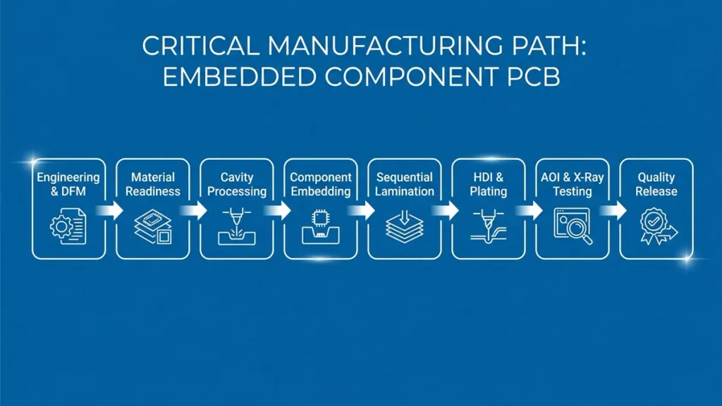
Critical Manufacturing Path Flowchart for Embedded Component PCB Lead Time
Embedded Component PCB Lead Time should be calculated from the manufacturing critical path, including engineering, material readiness, cavity processing, component embedding, lamination, HDI, finishing, inspection, and quality release.
A useful planning model is:
Total Lead Time = Critical Path Duration + Queue Time + Approval Time + Schedule Contingency
It is not always correct to simply add every individual process duration.
For example:
- Engineering review: 1–2 days
- Material preparation: 2–3 days
- Cavity processing: 1–3 days
- Embedding: 2–4 days
- Lamination: 3–5 days
- HDI processing: 2–5 days
- Finishing: 1–2 days
- Inspection/testing: 1–3 days
Some activities can overlap, while others cannot begin until previous operations are released.
Therefore, the critical path determines the actual shipment date.
What Happens During Embedded PCB Engineering and DFM?
Engineering review normally verifies:
- PCB data integrity
- Layer stack‑up
- Component dimensions
- Component orientation
- Cavity dimensions
- Cavity‑to‑copper clearance
- Component‑to‑component clearance
- Z‑height
- Prepreg thickness
- Resin‑flow conditions
- Microvia locations
- Via‑in‑pad structures
- Surface finish
- Testing requirements
This stage may take approximately 1–2 working days for a well‑prepared project.
Poorly prepared documentation can create multiple clarification cycles.
That is why complete manufacturing data can save more time than trying to negotiate one fewer production day.
How Does Component Availability Affect Embedded Component PCB Lead Time?
Component availability can become the longest lead‑time variable because an embedded PCB cannot enter its complete manufacturing route until the required components are available and technically approved.
Typical risks include:
- Long component manufacturer lead time
- End‑of‑life parts
- Allocation
- MOQ requirements
- Package changes
- Alternate‑component approval
- International shipping
- Customs clearance
- Incoming inspection
Sierra Circuits recommends checking component availability early, verifying the BOM, selecting qualified alternatives, and responding quickly to supplier questions because component sourcing can directly affect manufacturing schedules.
PCBWay also describes component sourcing routes involving local suppliers and international distributors, with additional time possible for international procurement and customs clearance.
For an embedded design, this issue is even more important because the component may become a structural element of the PCB fabrication process, rather than simply being installed after bare‑board fabrication.
How Can Procurement Teams Reduce Component‑Related PCB Delays?
Before releasing the PO, procurement should confirm:
- Manufacturer part number
- Approved manufacturer
- Component package
- Component dimensions
- Component height
- Availability
- Approved substitutes
- Quantity required
- Required delivery date
- Incoming inspection requirements
For high‑risk components, securing supply before PCB production is preferable to discovering a shortage after the laminate has already been prepared.
How Do Cavity Processing and Embedded Component Placement Affect PCB Lead Time?
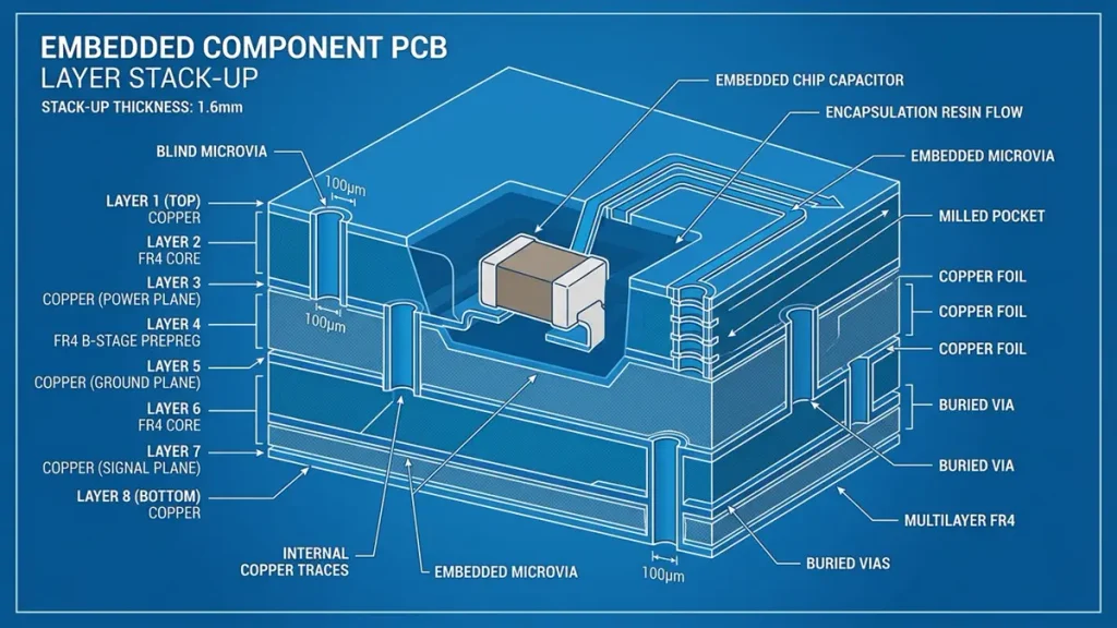
3D Technical Cross-Section Schematic of an Embedded Component PCB Layer Stack-Up
Cavity processing and component placement add manufacturing operations that do not exist in a conventional surface‑assembly workflow, making cavity geometry, positional accuracy, component dimensions, and fixation methods important lead‑time variables.
PCBWay describes embedded manufacturing as an integrated process in which component placement becomes part of PCB fabrication rather than remaining a completely separate assembly step.
A cavity may require:
- Mechanical routing
- Controlled‑depth machining
- Laser processing
- Cleaning
- Dimensional verification
- Component placement
- Fixation
- Resin/prepreg preparation
The actual process depends on the embedding architecture.
Würth Elektronik identifies several embedding approaches, including SOLDER.embedding, MICROVIA.embedding, FLIP‑CHIP.embedding, and COPPER.embedding, illustrating why different embedded structures can require substantially different process routes.
Why Can Component Placement Be More Difficult Than Conventional SMT?
A conventional surface‑mounted component remains visible and can be inspected after placement.
An embedded component may become inaccessible after lamination.
This changes the manufacturing philosophy.
Placement must consider:
- X/Y position
- Rotation
- Component height
- Pad geometry
- Cavity dimensions
- Pressure during processing
- Lamination movement
A published PCBWay technical discussion notes that embedded cavities may require very tight placement tolerances and that conventional SMT self‑alignment cannot necessarily compensate for the same level of placement error once the component is embedded.
This is an important reason why a supplier should not treat embedded component placement as ordinary SMT.
How Does Sequential Lamination Affect Embedded Component PCB Lead Time?
Sequential lamination can significantly extend the manufacturing route because the board may require several controlled build‑up and bonding operations rather than one conventional multilayer pressing cycle.
Additional cycles may require:
- Prepreg preparation
- Copper preparation
- Registration
- Controlled pressure
- Temperature profiling
- Resin flow management
- Cooling
- Post‑lamination inspection
The number of cycles depends on the stack‑up and embedding architecture.
A six‑layer embedded PCB and a 20‑layer embedded HDI PCB should therefore never be assigned the same manufacturing schedule simply because both contain embedded components.
How Do HDI and Microvias Affect Embedded Component PCB Lead Time?
HDI structures can increase lead time because laser drilling, desmear, copper plating, via filling, registration control, and sequential build‑up introduce additional dependent operations.
For advanced embedded PCB designs, the route may include: Laser drilling → Desmear → Electroless copper → Electroplating → Via filling → Imaging → Pattern plating → Etching
Additional HDI cycles create additional opportunities for:
- Registration variation
- Microvia defects
- Copper thickness variation
- Via‑fill problems
- Lamination distortion
- Inspection holds
The result is not necessarily a dramatic increase in machine time at each individual operation, but the total number of controlled operations increases.
Does mSAP Increase Embedded Component PCB Lead Time?
mSAP can add process complexity and inspection requirements, but it may be necessary when the embedded PCB requires fine‑line, high‑density routing that conventional subtractive processing cannot reliably support.
mSAP commonly involves:
- Seed‑layer preparation
- Imaging
- Selective copper plating
- Resist stripping
- Flash etching
- Final conductor formation
The lead‑time effect depends on:
- Line/space requirement
- Number of mSAP layers
- Copper thickness
- Registration requirements
- Plating process
- Inspection requirements
- Production capacity
Therefore, buyers should avoid assuming:
mSAP = automatically longer or: mSAP = automatically faster
The correct question is:
How does mSAP change the actual manufacturing route for this particular stack‑up?
How Do Advanced PCB Manufacturing Technologies Affect Embedded Component PCB Lead Time?
Advanced equipment does not simply make every process faster; its greater value is often improved process control, reduced external dependencies, faster setup, better registration, and earlier defect detection.
For an embedded PCB manufacturer, this can improve schedule predictability, which is often more valuable to procurement than a theoretical minimum production time.
How Does LDI Affect Embedded PCB Manufacturing Lead Time?
Laser Direct Imaging can support fine‑line pattern formation without relying on conventional photographic tooling for every image.
Potential schedule benefits include:
- Digital data transfer
- Faster engineering‑to‑imaging transition
- Improved registration control
- Reduced tooling dependency
- Better suitability for fine‑line structures
For an embedded PCB, registration consistency is particularly important because multiple internal structures must align with cavities and embedded components.
How Does Laser Drilling Affect Embedded PCB Lead Time?
Laser drilling provides a controlled process for microvia formation and certain high‑density structures.
For lead‑time management, the important benefits can include:
- In‑house process control
- Reduced outsourcing dependency
- Repeatable microvia formation
- Better production scheduling
- Faster engineering feedback
The technology should nevertheless be matched to the dielectric, copper construction, via diameter, depth, and required aspect ratio.
A supplier with the equipment but without a qualified process window does not automatically provide a shorter reliable lead time.
How Do AOI and X‑Ray Inspection Reduce Embedded PCB Delivery Risk?
AOI and X‑ray inspection can reduce late‑stage schedule risk by identifying defects before a problematic lot progresses further or is shipped.
AOI can identify visible pattern‑related defects such as:
- Opens
- Shorts
- Missing copper
- Pattern abnormalities
- Registration‑related issues
X‑ray can provide visibility into structures that cannot be visually inspected after embedding.
This is particularly relevant because embedded components may be hidden inside the finished multilayer structure.
The objective is therefore not simply: “inspect faster.”
It is: “detect critical defects before they become expensive downstream failures.”
What Manufacturing Problems Can Delay Embedded Component PCB Delivery?
The most serious delays usually come from engineering changes, material shortages, component shortages, cavity defects, lamination problems, hidden interconnect defects, inspection failures, and low first‑pass yield.
What Happens When Embedded Components Move During Lamination?
If component position changes beyond the acceptable manufacturing window, the resulting geometry can affect:
- Electrical connections
- Clearance
- Microvia alignment
- Pad access
- Cavity integrity
A board may then require engineering disposition, additional inspection, rework, or remake.
How Do Resin Voids Create Embedded PCB Lead‑Time Risk?
Resin flow around an embedded component must be compatible with the cavity geometry and component profile.
Poor resin distribution can result in:
- Voids
- Local delamination risk
- Incomplete encapsulation
- Mechanical stress concentration
The key manufacturing challenge is not merely filling the cavity. It is achieving consistent material distribution under the selected lamination profile.
How Can PCB Warpage Delay Delivery?
Warpage can emerge from differences in:
- Copper distribution
- Laminate construction
- Component geometry
- Resin content
- Thermal expansion
- Lamination conditions
A board may pass electrical testing but still require additional dimensional evaluation before shipment.
Why Are Hidden Defects a Serious Embedded PCB Schedule Risk?
This is one of the fundamental differences between embedded and conventional PCB manufacturing.
A surface‑mounted defect can often be visually inspected.
An embedded defect may be physically hidden after the final lamination cycle.
Therefore, the cost of late detection can be high.
From a manufacturing perspective, the most dangerous lead‑time problem is not a process that takes one extra day. It is a defect discovered after the board has already passed through several high‑value downstream operations.
That is why process control and early inspection directly influence delivery reliability.
What Does an Embedded Component PCB Manufacturing Schedule Look Like?
A practical production schedule can be divided into engineering, material preparation, cavity processing, embedding, lamination, HDI/fine‑line processing, finishing, testing, and final quality release.
| Manufacturing Stage | Standard Planning | Possible Expedited Planning | Typical Activities |
|---|---|---|---|
| Engineering & DFM | 1–2 days | 4–12 hours | Data verification, stack‑up, cavity review |
| Materials & preparation | 2–3 days | 1–2 days | Laminate, copper, prepreg preparation |
| Cavity processing | 1–3 days | 1–2 days | Routing/laser/depth‑controlled processing |
| Component embedding | 2–4 days | 1–2 days | Placement, fixation, pre‑lamination preparation |
| Lamination & build‑up | 3–5 days | 2–3 days | Controlled lamination/sequential build‑up |
| HDI / fine‑line processing | 2–5 days | 1–3 days | Laser drilling, plating, imaging |
| Surface finishing | 1–2 days | ~1 day | Solder mask, surface finish |
| Inspection & testing | 1–3 days | ~1 day | AOI, X‑ray, electrical test |
| Quality release | 0.5–1 day | Same day where qualified | Final inspection and documentation |
Important: These are planning ranges, not guaranteed production times. Some operations can overlap, while others are strictly dependent on previous process completion.
The supplier should provide the actual schedule after reviewing the design.
Why Is Waiting Time Important When Estimating Embedded PCB Lead Time?
Waiting time can become a major portion of total lead time because materials, components, engineering approvals, production slots, external processes, and quality decisions may occur outside the nominal machine‑processing time.
Consider a simplified example.
A PCB may require only: 12 days of actual processing but still have a: 18‑day total delivery schedule
because six additional days are consumed by:
- Material waiting
- Component arrival
- Production queue
- Engineering approval
- Testing slot
This is why procurement should ask suppliers for: “What is the total committed lead time, and what assumptions does it depend on?”
rather than simply: “How many days does fabrication take?”
How Can Buyers Reduce Embedded Component PCB Lead Time?
The fastest way to reduce lead time is usually to remove avoidable waiting and engineering iterations before production starts.
Before RFQ
Prepare:
- Gerber or ODB++
- BOM
- Stack‑up
- Embedded component placement data
- Component MPN
- Component dimensions
- Component height
- Cavity drawings
- Quantity
- Surface finish
- HDI requirements
- Testing requirements
During DFM
Confirm:
- Cavity clearance
- Component orientation
- Component‑to‑copper spacing
- Prepreg thickness
- Resin‑flow conditions
- Microvia locations
- Via‑fill requirements
- Lamination sequence
Before PO Release
Confirm:
- Material availability
- Component availability
- Approved substitutes
- Manufacturing capacity
- Testing capacity
- Target shipment date
- Expedited options
- Engineering change procedure
This approach can eliminate several common sources of schedule uncertainty.
How Should Buyers Compare Embedded Component PCB Supplier Lead Times?
Buyers should compare suppliers based on the reliability and definition of their lead‑time commitment, not simply the smallest number of days in a quotation.
A useful supplier comparison includes:
| Procurement Question | What a Strong Supplier Should Provide |
|---|---|
| When does lead time start? | Clearly defined starting point |
| Are materials available? | Material confirmation |
| Are components available? | BOM/component verification |
| Has DFM been completed? | Engineering feedback |
| Is the process in‑house? | Clear manufacturing route |
| Is capacity reserved? | Production scheduling |
| What inspections are included? | Defined QC plan |
| What can cause delay? | Risk disclosure |
| What happens after an engineering change? | Schedule impact assessment |
| Is expedited production possible? | Feasibility‑based answer |
A short quoted lead time without these details may create more procurement risk than a slightly longer but well‑controlled schedule.
What Should Procurement Ask an Embedded Component PCB Manufacturer Before Placing an Order?
Procurement should ask the manufacturer to define the manufacturing route, lead‑time assumptions, material status, component status, inspection scope, and conditions that could change the shipment date.
Ask these questions:
- What is the lead time from PO to shipment?
- Does your quoted lead time include material procurement?
- Are the embedded components in stock?
- Has engineering completed DFM?
- How many lamination cycles are required?
- Which processes are performed in‑house?
- What inspection is used for embedded structures?
- Is X‑ray inspection available?
- What is the expected prototype lead time?
- What is the repeat‑production lead time?
- What conditions trigger a schedule revision?
- Can production capacity be reserved after PO approval?
These questions move the procurement discussion from price‑only sourcing to total delivery risk management.
How Does Shenzhen Hongda Circuit Technology Support Embedded Component PCB Lead Time?
Shenzhen Hongda Circuit Technology Co., Ltd. approaches embedded PCB lead time by combining engineering review, controlled PCB fabrication, advanced imaging and drilling processes, automated inspection, and production scheduling to reduce avoidable process and communication delays.
Our manufacturing approach can incorporate advanced PCB technologies such as:
- HDI manufacturing
- Laser microvia drilling
- LDI
- Fine‑line circuit formation
- mSAP‑compatible manufacturing routes where required
- Sequential multilayer build‑up
- Controlled lamination
- AOI inspection
- X‑ray inspection
- Electrical testing
- High‑density multilayer fabrication
The value of these technologies is not simply equipment speed.
For embedded PCB projects, process integration is often more important.
A lead‑time‑efficient manufacturing route should minimize unnecessary handoffs between: Engineering → Material → Cavity → Embedding → Lamination → HDI → Inspection
When these operations are properly coordinated, the manufacturer can identify potential schedule risks earlier.
For example, if an embedded component requires a particular cavity depth and a microvia must subsequently land within a tight positional window, the engineering team should identify that relationship before the board enters mass production.
That is where manufacturing experience becomes relevant to lead time.
Why Does In‑House Process Control Matter for Embedded PCB Delivery?
When critical processes are controlled within the manufacturing workflow, the supplier has greater visibility into:
- Production queues
- Process status
- Engineering changes
- Inspection results
- Rework decisions
- Capacity allocation
This can reduce dependency on external processing schedules.
However, equipment alone should never be presented as a guarantee of faster delivery.
The correct procurement question is:
Can the manufacturer demonstrate that its equipment, process controls, inspection system, and capacity planning are suitable for my specific embedded PCB?
That is a much stronger supplier‑selection criterion.
What Is the Difference Between a Fast Embedded PCB Supplier and a Reliable One?
A fast supplier offers a short nominal schedule; a reliable supplier can explain, control, and monitor the manufacturing conditions required to achieve that schedule.
For example:
Supplier A: “Your board can be completed in 7 days.”
Supplier B: “Your board requires two lamination cycles, laser microvias, embedded component placement, X‑ray inspection, and a specialty dielectric. Based on current material availability and production capacity, we estimate 16 working days from engineering release to shipment.”
For a procurement manager, Supplier B may actually represent the lower‑risk choice.
The shortest number is not always the shortest reliable lead time.
How Should Buyers Handle Expedited Embedded Component PCB Orders?
Expedited production should be evaluated after the manufacturer confirms design complexity, material readiness, component availability, production capacity, and inspection requirements.
A possible expedited target for qualified designs is: 7–10 working days
but it should not be treated as a universal embedded‑PCB standard.
Expedited manufacturing becomes more realistic when:
- Components are already available
- Laminate is in stock
- Engineering data is frozen
- Standardized materials are used
- Production capacity is available
- Testing requirements are known
- No major engineering change is expected
Trying to compress every process simultaneously can increase manufacturing risk.
For high‑value prototypes, the better strategy may be: Prototype → Engineering Validation → Pilot Build → Volume Production
rather than forcing the entire production order into an aggressive schedule.
How Can Buyers Build a More Reliable Embedded PCB Delivery Plan?
A reliable delivery plan should include both the manufacturing schedule and the risks that could change the schedule.
A practical procurement plan should define:
1. Engineering release date ↓ 2. Material availability date ↓ 3. Component availability date ↓ 4. Production start ↓ 5. Embedding completion ↓ 6. Lamination completion ↓ 7. HDI/fine‑line completion ↓ 8. Inspection completion ↓ 9. Quality release ↓ 10. Shipment date
This milestone‑based approach provides much better visibility than a single statement such as:
“Lead time: 15 days.”
What Information Is Needed for an Accurate Embedded Component PCB Lead Time Quote?
The more complete the manufacturing package, the more accurately a supplier can calculate the actual production route and delivery date.
Send the supplier:
PCB Design Files
- Gerber
- ODB++
- NC drill files
- Stack‑up
- Fabrication drawing
- Board dimensions
Embedded Component Information
- BOM
- Manufacturer part number
- Datasheet
- X/Y location
- Rotation
- Component dimensions
- Component height
- Cavity information
Manufacturing Requirements
- Layer count
- Finished thickness
- Copper thickness
- HDI structure
- Microvia dimensions
- Via filling
- mSAP requirements
- Surface finish
- Solder mask requirements
Quality Requirements
- AOI
- X‑ray
- Electrical test
- Cross‑section
- Reliability testing
- Inspection reports
- Certification requirements
With these inputs, an engineering team can evaluate the actual manufacturing path instead of estimating from incomplete information.
What Are the Most Common Embedded Component PCB Lead‑Time Mistakes?
The most common mistakes are incomplete RFQ files, unclear component availability, unverified stack‑ups, late engineering changes, unrealistic expedited schedules, and comparing embedded PCB lead times with standard PCB quick‑turn times.
Mistake 1: Comparing Only the Final Number
“10 days” versus “15 days” tells you little unless the starting conditions are identical.
Mistake 2: Ignoring Component Lead Time
A PCB manufacturer cannot complete an embedded build if the required component is unavailable.
Mistake 3: Changing the Stack‑Up After PO
A stack‑up change can affect:
- Lamination
- Material
- Impedance
- Cavity
- Microvias
- Finished thickness
It may require engineering requalification.
Mistake 4: Treating Embedded Placement Like Conventional SMT
The component may become inaccessible after lamination, making placement accuracy and process control more important.
Mistake 5: Asking for Expedited Production Too Late
If materials and components have not been reserved, an “urgent” production request may not actually be executable.
How Can an Embedded Component PCB Manufacturer Help Prevent Delivery Delays?
The manufacturer should identify schedule‑critical risks before production begins and communicate their impact before they become manufacturing problems.
A strong engineering workflow should include:
Design Review → Identify manufacturability risks
BOM Review → Identify component availability risks
Material Review → Identify laminate/prepreg risks
Process Review → Identify cavity, embedding, lamination and HDI risks
Capacity Review → Confirm realistic production slot
Inspection Review → Define how hidden structures will be verified
Schedule Review → Establish a realistic shipment commitment
This approach transforms lead time from a simple sales number into an engineering‑controlled process.
How Can You Get an Accurate Embedded Component PCB Lead Time Quote?
Submit the complete PCB design package, BOM, embedded‑component information, quantity, material requirements, and testing requirements so the manufacturer can evaluate the complete manufacturing route.
For a professional RFQ, include:
- Gerber/ODB++
- BOM
- Stack‑up
- Embedded component placement
- Component MPN
- Component dimensions
- Cavity requirements
- Quantity
- Material requirements
- HDI/mSAP requirements
- Surface finish
- Testing requirements
- Target delivery date
Shenzhen Hongda Circuit Technology Co., Ltd. can review the manufacturing requirements and determine the practical production route for your embedded PCB project.
For project‑specific lead‑time evaluation: Website: www.pcbkr.com Email: pcb@pcbkr.com
What Should Procurement Teams Remember About Embedded Component PCB Lead Time?
The most reliable way to control Embedded Component PCB Lead Time is to manage the complete manufacturing critical path rather than selecting a supplier solely on the shortest advertised turnaround.
For procurement teams, five principles are particularly important:
- Define exactly when lead time starts.
- Confirm component and material availability before production.
- Evaluate the complete manufacturing route, including embedding, lamination, HDI, and inspection.
- Ask what equipment and processes are controlled in‑house.
- Compare delivery reliability, not just the shortest quoted number.
A well‑managed embedded PCB project can achieve a predictable delivery schedule even when the manufacturing route is considerably more complex than a conventional multilayer PCB.
At Shenzhen Hongda Circuit Technology Co., Ltd., our objective is to make the quoted lead time traceable to the actual engineering and manufacturing conditions of the project—not simply to provide an attractive number on an RFQ.
Embedded Component PCB Lead Time FAQ for Procurement Teams
What Is the Typical Embedded Component PCB Lead Time?
Standard embedded PCB projects commonly require about 10–20 working days, while complex HDI, mSAP, specialty‑material, or multi‑lamination designs may require 15–30+ working days. Expedited schedules around 7–10 working days may be feasible for qualified projects with materials, components, engineering data, and production capacity ready.
The actual schedule should always be confirmed against the specific manufacturing route.
How Fast Can an Embedded PCB Manufacturer Deliver?
Some qualified embedded PCB projects may be produced on an expedited schedule of approximately 7–10 working days, but this depends on design complexity, material availability, component readiness, production capacity, and testing requirements.
A supplier should confirm feasibility after reviewing the actual files rather than promising an aggressive schedule before engineering review.
What Causes Embedded Component PCB Lead‑Time Delays?
The most common causes are component shortages, material shortages, incomplete engineering data, late design changes, cavity‑processing problems, lamination issues, HDI/microvia defects, inspection failures, and production capacity constraints.
For embedded designs, defects discovered after lamination can be particularly costly because the embedded structure may no longer be directly accessible.
What Information Does a Buyer Need to Get an Accurate Embedded PCB Lead‑Time Quote?
Provide Gerber or ODB++ files, BOM, stack‑up, embedded component locations, component manufacturer part numbers, component dimensions and height, cavity requirements, quantity, material specifications, HDI requirements, surface finish, and testing requirements.
The more complete the RFQ package, the less time is normally lost to engineering clarification.
How Should I Choose an Embedded Component PCB Manufacturer for Reliable Lead Time?
Evaluate the supplier’s engineering capability, in‑house manufacturing processes, laser drilling and HDI capability, LDI/fine‑line capability, lamination control, AOI/X‑ray inspection, material and component sourcing, production capacity, and ability to provide a milestone‑based delivery schedule.
Do not select a supplier solely because it advertises the lowest number of production days.
A reliable supplier should be able to explain why the quoted lead time is achievable and what conditions could change it.
Final Procurement Checklist
Before approving an embedded PCB supplier, ask:
- Is the lead time measured from PO, engineering approval, or material readiness?
- Are embedded components available?
- Are materials available?
- Has DFM been completed?
- How many lamination cycles are required?
- Are cavity and microvia processes qualified?
- Are critical processes performed in‑house?
- Is LDI available for high‑density imaging?
- Is laser drilling available for required HDI structures?
- Are AOI and X‑ray inspection available?
- Is the production slot confirmed?
- Is there a documented escalation process for delays?
- Can the supplier support prototype, pilot, and production phases?
If the supplier cannot answer these questions clearly, the quoted lead time should be treated as an estimate rather than a controlled delivery commitment.
Need a project‑specific Embedded Component PCB Lead Time evaluation? Send your Gerber/ODB++, BOM, stack‑up, embedded component details, quantity, and target delivery date to Shenzhen Hongda Circuit Technology Co., Ltd.
Website: www.pcbkr.com Email: pcb@pcbkr.com
About Author
David Chen https://www.linkedin.com/in/pcbcoming
David Chen boasts an extensive professional background in PCBA manufacturing, PCBA testing, and PCBA optimization, with specialized expertise in high-precision PCBA fault analysis and rigorous PCBA reliability testing. The author has worked with high-layer-count server PCB fabrication, ultra-low-loss backplane stackups, and thermo-mechanical reliability optimization for AI infrastructure projects involving 112G and 224G PAM4 architectures. Skilled in complex circuit design and cutting-edge advanced PCB manufacturing processes, he delivers solutions that elevate product durability and performance across industrial applications. His technical articles focusing on PCBA manufacturing workflows and testing methodologies are widely cited by industry peers, research institutions, and technical platforms, solidifying his reputation as a recognized technical authority in the global circuit board manufacturing sector.