Embedded Component PCB Price: Cost Factors, Pricing, and Cost Reduction
Embedded Component PCB Price depends on far more than simple board dimensions and layer quantity. Multiple critical factors drive final costs, including embedded component type, cavity design complexity, component Z‑height requirements, HDI build structures, repeated lamination cycles, base material selection, specialized inspection procedures, custom tooling, production volume, and expected manufacturing yield. To build reliable project budgets, PCB buyers need to evaluate the total cost per fully functional, acceptable board, instead of relying solely on bare unit price for cost comparison.
This article targets procurement and sourcing teams. It focuses on real‑world quoting, RFQ requirements, TCO calculation, yield‑adjusted cost and supplier comparison. For deep‑dive technical analysis on stack‑up, lamination and DFM principles, refer to our engineer‑oriented technical article.
How Much Does an Embedded Component PCB Cost?
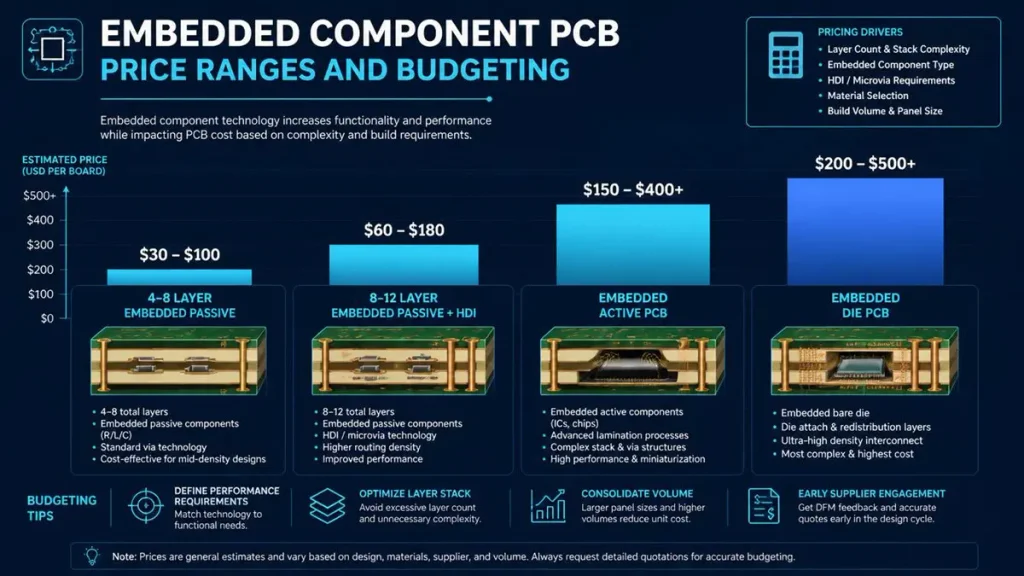
Embedded Component PCB Price Ranges & Budgeting Infographic
A preliminary prototype budget is typically around US$30–150 per board for simpler embedded-passive designs and approximately US$150–500+ for more complex HDI, embedded-active, embedded-die, high-layer-count, or specialty-material designs. Actual pricing depends on the complete PCB design, embedded components, manufacturing process, quantity, testing, and yield.
| Embedded PCB configuration | Preliminary prototype budget* | Main cost sensitivity |
|---|---|---|
| 4–8 layer embedded passive PCB | US$30–100 | Components and cavity processing |
| 8–12 layer embedded passive + HDI | US$60–180 | HDI and lamination |
| 12–16 layer embedded + HDI | US$100–300 | Sequential build-up |
| Embedded active component PCB | US$150–400+ | Interconnection and thermal requirements |
| Embedded die PCB | US$200–500+ | Advanced component integration |
| Specialty-material embedded PCB | US$150–500+ | Material and qualification |
These figures are preliminary budgeting ranges rather than fixed market prices. PCB dimensions, component cost, cavity structure, materials, panel utilization, inspection, testing, production volume, and supplier process capability can change the actual quotation.
For procurement, the more useful calculation is:
Cost per accepted board = Total manufacturing spend ÷ Accepted boards
This is particularly important for embedded component PCBs because a rejected board may already contain expensive components and several completed manufacturing processes.
Why Does an Embedded Component PCB Cost More Than a Conventional PCB?
An embedded component PCB can cost more because the component becomes part of the internal PCB structure, adding requirements for component integration, cavity formation, lamination, internal interconnection, registration, inspection, and yield control.
A conventional PCB quotation is often influenced primarily by:
- Board size
- Layer count
- Copper thickness
- Material
- Surface finish
- Quantity
- Trace and space
- Hole structure
An embedded component PCB can introduce additional cost variables:
- Component type
- Component dimensions
- Component Z-height
- Cavity dimensions
- Cavity depth
- Component-to-cavity clearance
- Internal interconnection
- Microvia structure
- Sequential lamination
- Hidden-structure inspection
- Reliability requirements
Therefore, two boards with exactly the same dimensions and layer count can have very different prices.
For example:
PCB A
- 8 layers
- 4 embedded passive components
- One cavity family
- Moderate HDI
- Conventional high-Tg FR-4
PCB B
- 8 layers
- 16 embedded components
- Multiple cavity families
- Tight component clearance
- Stacked microvias
- Via-in-pad
- Specialty dielectric
- Expanded X-ray inspection
The physical dimensions may be similar, but the manufacturing cost structure is substantially different.
The key principle is:
Same PCB dimensions do not mean the same manufacturing cost.
What Are the Biggest Embedded Component PCB Cost Drivers?
The major cost drivers are embedded component type, production quantity, manufacturing yield, sequential lamination, HDI complexity, material selection, cavity design, tooling, and inspection requirements.
A practical cost hierarchy is:
High-impact cost drivers
- Embedded component type
- Production volume
- Manufacturing yield
- Sequential lamination
- HDI and microvia density
- Material selection
Medium-impact cost drivers
- Cavity quantity
- Cavity dimensions
- Cavity depth
- Cavity tolerance
- Copper thickness
- Via filling
- Internal registration
- Inspection requirements
Lower-impact cost drivers
- Surface finish
- Solder mask
- Silkscreen
- Packaging
- Minor mechanical features
These factors interact with one another.
For example:
More layers + more sequential builds + more microvias + tighter tolerances
can create a much larger cost increase than any individual parameter.
Similarly:
Tighter cavity tolerance → smaller process window → additional process control → increased inspection → greater yield exposure
This is why embedded PCB cost optimization should evaluate the complete manufacturing route instead of negotiating individual line items.
How Does the Embedded Component Type Affect PCB Price?
Embedded passive components, active components, and semiconductor dies can create very different cost structures because they require different levels of handling, alignment, interconnection, thermal management, and inspection.
A simplified progression is:
Embedded passive
Component placement → embedding → lamination → interconnection
versus:
Embedded active or die
Component handling → precision placement → specialized interconnection → thermal considerations → additional inspection → reliability validation
The direct component price is only one part of the equation.
An active device or semiconductor die can also affect:
- Pad architecture
- Placement tolerance
- Cavity dimensions
- Dielectric construction
- Interconnection design
- Thermal path
- Inspection
- Reliability validation
This is why an accurate RFQ should include the actual manufacturer part number, package dimensions, terminal structure, and component Z-height.
How Does Component Z-Height Affect Embedded PCB Cost?
Component Z-height can affect dielectric thickness, cavity depth, stack-up construction, lamination conditions, and dimensional control, making it an important embedded PCB cost variable.
Consider two components:
- Component A: 0.30 mm Z-height
- Component B: 0.80 mm Z-height
If both are embedded into the same general PCB region, the second component may require a different dielectric and cavity configuration.
The situation becomes more complicated when a PCB contains multiple component heights, such as:
0.30 mm + 0.50 mm + 0.80 mm + 1.00 mm
Different heights can require different internal structures.
That may increase:
- Engineering preparation
- Material combinations
- Lamination complexity
- Dimensional control
- Inspection requirements
- Yield risk
A practical engineering rule is:
Do not quote an embedded PCB from the BOM reference alone.
For more accurate pricing, provide:
Part number + package dimensions + terminal structure + Z-height + mounting orientation
How Does Cavity Complexity Increase Embedded Component PCB Price?
Cavity-related cost increases with cavity quantity, geometry diversity, depth variation, dimensional tolerance, clearance requirements, and inspection requirements.
Cavity complexity can be evaluated using several parameters.
| Parameter | Lower-complexity example | Higher-complexity example |
|---|---|---|
| Cavity count | 4 | 20 |
| Cavity depth | 300 µm | 300–800 µm |
| Depth tolerance | ±50 µm | ±20 µm |
| Cavity families | 1–2 | 5–6 |
| Component clearance | 150 µm | 50 µm |
| Inspection | Sampling | Expanded inspection |
These values are engineering examples rather than universal manufacturing limits.
An important distinction is the difference between cavity quantity and cavity diversity.
Twenty identical cavities may be easier to manufacture than six cavities with different geometries, depths, and tolerance requirements.
This means:
Cavity diversity can be a stronger cost driver than cavity count alone.
Manufacturing pain point: unnecessary tolerance
One common engineering problem is specifying an extremely tight cavity tolerance because it is technically possible rather than because the product function requires it.
For example, if the component interface can function with:
±50 µm
but the drawing specifies:
±20 µm
the tighter tolerance may narrow the manufacturing process window without providing additional product value.
A better question is:
What tolerance does the functional interface actually require?
That question can create a meaningful cost-reduction opportunity before production begins.
How Do HDI and Microvias Affect Embedded Component PCB Cost?
HDI and microvia structures increase cost through laser drilling, dielectric processing, desmear, metallization, plating, via filling, registration control, and additional inspection.
A design can move from:
Moderate HDI
to:
Dense HDI + stacked microvias + via-in-pad + copper-filled vias
and experience a significant increase in process complexity.
| Interconnection structure | Example process burden |
|---|---|
| Moderate microvia structure | Lower |
| Dense HDI | Medium |
| Stacked microvias | Higher |
| Stacked microvias + via-in-pad + copper filling | Higher still |
The actual price depends on:
- Microvia diameter
- Dielectric thickness
- Aspect ratio
- Via depth
- Via count
- Stacking level
- Copper filling
- Registration tolerance
- Reliability requirements
Microvia pricing should therefore not be treated simply as a laser-drilling cost.
A more realistic model is:
Microvia cost = fabrication + inspection + reliability exposure
If a buried interconnection requires additional inspection or reliability validation, those costs should be considered in the quotation.
How Does Sequential Lamination Change Embedded PCB Pricing?
Additional sequential lamination cycles can increase material handling, pressing, registration, drilling, plating, inspection, cycle time, and yield exposure.
A simplified manufacturing route may look like:
Core
→ dielectric build-up
→ laser drilling
→ metallization
→ additional dielectric build-up
→ laser drilling
→ plating
→ outer-layer processing
The important pricing question is therefore not simply:
“How many layers does the PCB have?”
It is:
“How many manufacturing cycles are required to create the specified internal structure?”
For example, two 10-layer PCBs can have very different costs:
Design A
- 10 layers
- simpler lamination structure
- moderate blind vias
Design B
- 10 layers
- multiple sequential build-up cycles
- stacked microvias
- via-in-pad
- copper-filled vias
The layer count is identical.
The manufacturing route is not.
An experienced cost review should therefore ask:
Can the same electrical function be achieved with fewer sequential build-up operations?
Sometimes adding a routing layer can reduce total cost if it eliminates an expensive interconnection structure.
How Do PCB Materials Affect Embedded Component PCB Price in 2026?
Material selection can substantially affect embedded PCB pricing, particularly when the design requires high-Tg, low-loss, low-CTE, specialty dielectric systems, low-profile copper, or other high-performance materials.
Potentially cost-sensitive material choices include:
- Standard FR-4
- High-Tg FR-4
- Low-loss laminates
- Very-low-loss laminates
- Specialty dielectric materials
- Embedded-resistor materials
- Low-profile copper foil
- High-conductivity copper
For high-speed applications, the material decision should be based on the actual electrical requirement rather than simply selecting the most expensive available laminate.
A practical strategy can be:
Critical high-speed layers → higher-performance material
Less demanding layers → qualified lower-cost material
However, any material combination must be evaluated for:
- Electrical compatibility
- Thermal behavior
- Lamination compatibility
- Mechanical behavior
- Reliability
- Availability
Why does material availability matter to price?
Material availability has become an increasingly important commercial issue.
Würth Elektronik has reported supply pressure involving CCL, copper foils, prepregs and high-performance resin, with potential effects on pricing, lead times, and quotation predictability.
For procurement, this means an RFQ should specify:
- Material manufacturer
- Material grade
- Electrical requirements
- Copper foil requirements
- Approved alternatives
- Quotation validity
- Material availability
A quotation without clearly defined material assumptions can become difficult to compare.
How Does Resin Flow Create Hidden Embedded PCB Costs?
Embedded components change the internal geometry of the laminate stack, making resin flow, dielectric thickness, cavity depth, component height, and copper distribution important factors in manufacturing yield.
A useful engineering relationship is:
Component Z-height + Cavity depth + Prepreg thickness + Copper distribution + Resin flow
These parameters influence the final laminated structure.
Potential manufacturing problems include:
- Resin starvation
- Voids
- Uneven dielectric thickness
- Component movement
- Localized stress
- Lamination deformation
Manufacturing scenario
Imagine a panel where several embedded components are concentrated in one region.
That region may have a different copper distribution from the surrounding PCB.
During lamination, the local structure can respond differently.
If the dielectric system and pressing conditions are not properly matched, the result may include:
- Thickness variation
- Voids
- Dimensional movement
- Localized mechanical stress
The financial problem is that these defects may be discovered after multiple expensive processes have already been completed.
This is why early engineering review can save more money than a small reduction in the final quoted unit price.
How Does Manufacturing Yield Change the Real Embedded PCB Cost?
Manufacturing yield can significantly change the effective cost because every rejected board represents consumed material, components, processing time, inspection, and capacity.
The basic calculation is:
Required input = Required good units ÷ Yield
For 10,000 accepted boards:
At 98% yield:
10,000 ÷ 0.98 = 10,204 boards
At 90% yield:
10,000 ÷ 0.90 = 11,111 boards
That is approximately 907 additional input boards.
Those additional units can consume:
- Laminate
- Embedded components
- Copper
- Prepreg
- Laser processing
- Plating
- Inspection
- Electrical testing
- Labor
A useful first-level comparison is:
Effective manufacturing cost = Quoted cost ÷ Yield
This is not a complete TCO calculation, but it is a useful way to identify why a lower quotation does not always produce lower production cost.
How Does Late-Stage Scrap Increase Embedded PCB Cost?
The later a defect is discovered, the more manufacturing value may already be embedded in the rejected board.
A typical value accumulation sequence is:
Raw laminate
↓
Inner-layer fabrication
↓
Component preparation
↓
Embedding
↓
Lamination
↓
Laser drilling
↓
Plating
↓
Outer-layer processing
↓
Inspection
↓
Electrical test
A defect detected at the raw-material stage has a very different economic impact from one detected after plating and final inspection.
A practical scrap model is:
Scrap cost = Material + Component + Completed processing + Inspection
This is one reason embedded PCB manufacturers need effective internal process controls rather than relying only on final electrical testing.
For procurement, this also means that yield and process stability deserve attention during supplier evaluation.
How Do NRE and Tooling Affect Embedded Component PCB Prototype Pricing?
NRE and tooling can dominate prototype unit economics because fixed costs are distributed across a small number of boards.
Use:
Unit cost = Variable manufacturing cost + (NRE + tooling) ÷ Quantity
For example, if:
NRE + tooling = US$3,000
then the fixed-cost allocation is:
| Quantity | NRE + tooling allocation |
|---|---|
| 10 boards | US$300/board |
| 100 boards | US$30/board |
| 1,000 boards | US$3/board |
| 10,000 boards | US$0.30/board |
This is an illustrative calculation, not a standard supplier fee.
It explains why a prototype quotation can appear expensive while the production unit price becomes substantially lower.
For procurement, request separate pricing for:
- Engineering/NRE
- Tooling
- PCB fabrication
- Embedded components
- Inspection
- Testing
This makes prototype and production economics much easier to compare.
How Does Production Volume Change Embedded Component PCB Unit Price?
Increasing production volume generally reduces the per-unit allocation of NRE, tooling, setup, and engineering costs, while improving material and component purchasing efficiency.
Prototype
20 boards
The major issue is fixed-cost allocation.
Pilot production
500 boards
The major issue becomes process stability and yield.
Production
10,000 boards
Recurring manufacturing cost, panel utilization, material purchasing, and yield become more important.
High-volume production
50,000+ boards
Supply continuity, component sourcing, process control, yield, and manufacturing capacity become increasingly important.
The important principle is:
Low unit price does not automatically mean low total cost.
A supplier offering a low nominal price but unstable production yield may generate a higher effective cost.
How Does Panel Utilization Affect Embedded Component PCB Price?
Better panel utilization can reduce the manufacturing cost allocated to each PCB, especially for small and medium-sized boards.
Consider an illustrative comparison:
Panel A: 8 boards
Panel B: 12 boards
The second panel contains:
50% more boards per panel
However, this does not mean the PCB automatically becomes 50% cheaper.
Panelization must account for:
- Board outline
- Component position
- Cavity location
- Copper balance
- Tooling rails
- Test coupons
- Routing
- V-scoring
- Electrical test
- Manufacturing orientation
Embedded components can restrict panelization because cavity and component locations may prevent simple rotation or nesting.
Therefore, panel utilization should be optimized together with the internal component architecture.
What Hidden Manufacturing Problems Can Increase Embedded PCB Cost?
The most expensive hidden costs usually come from defects that are difficult to detect early and are discovered after substantial manufacturing value has already been added.
Component-to-cavity misregistration
The component may be correctly positioned relative to the placement program but incorrectly positioned relative to:
- Cavity walls
- Internal pads
- Microvias
- Routing features
The result can be scrap or rework.
Lamination movement
Thermal and mechanical movement can change internal registration.
Potential result:
Misregistration → interconnection defect → rejection
Resin voiding
Voids around an embedded component can create mechanical or thermal reliability concerns.
Microvia defects
A buried interconnection problem may remain invisible from the external surface.
Cavity dimensional drift
Cavity depth or dimensions outside the functional window can affect component fit and lamination.
Hidden internal defects
Surface inspection cannot reveal every internal structure.
Depending on the design, additional inspection may include:
- X-ray
- 3D inspection
- Electrical testing
- Cross-section analysis
The important pricing relationship is:
More complex hidden structures → greater inspection requirements → greater manufacturing cost
How Can Engineers Reduce Embedded Component PCB Cost Without Sacrificing Quality?
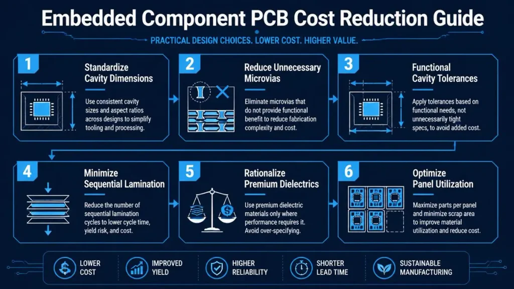
6-Step Embedded Component PCB Cost Reduction Guide
embedded-component-pcb-cost-reduction-guide-flowchart
The best cost reductions usually come from removing unnecessary process complexity rather than reducing material quality or eliminating required inspection.
1. Standardize cavity dimensions
Where component packages permit it, common cavity dimensions can simplify manufacturing.
2. Reduce unnecessary microvias
Review whether every microvia is functionally required.
3. Evaluate staggered versus stacked vias
A simpler via architecture may reduce process complexity when electrical requirements permit.
4. Use functional tolerances
Avoid specifying unnecessarily tight tolerances.
5. Reduce sequential lamination
Review whether the same electrical architecture can be achieved with fewer build-up cycles.
6. Rationalize premium materials
Use high-performance materials where their properties are actually required.
7. Improve panel utilization
Optimize board arrangement around the actual cavity and component architecture.
8. Review component sourcing
Where the design allows, qualify alternative components before supply constraints become a cost problem.
The objective is:
Required performance + qualified reliability + predictable yield + controlled manufacturing cost
rather than simply:
Lowest initial quotation
Which Embedded PCB Specifications Should Buyers Challenge During a Cost Review?
Buyers should challenge specifications that significantly reduce the manufacturing process window without delivering a measurable electrical, mechanical, thermal, or reliability benefit.
| Specification | Cost-review question |
|---|---|
| Cavity tolerance | Is this tolerance functionally necessary? |
| Line/space | Does every PCB region require the same geometry? |
| Microvia count | Can some vias be eliminated? |
| Via architecture | Can stacked vias become staggered? |
| Layer count | Would another layer actually simplify manufacturing? |
| Lamination | Can one build-up cycle be removed? |
| Material | Does every layer require premium material? |
| Copper thickness | Is the specified thickness required everywhere? |
| Inspection | What defects must the inspection actually detect? |
| Panelization | Is the panel arrangement production-efficient? |
The best cost-engineering question is:
Which specification is creating the largest manufacturing cost, and what is the least expensive qualified alternative?
That question produces more useful results than simply asking a supplier to lower the quotation.
How Should Buyers Calculate the Total Cost of an Embedded Component PCB?
Buyers should compare total cost of ownership and calculate the effective cost per accepted board.
A practical model is:
TCO = PCB + Components + NRE + Tooling + Testing + Scrap + Logistics + Engineering
Then:
TCO per good board = Total TCO ÷ Accepted units
Example
Assume two hypothetical quotations:
Supplier A
- PCB price: US$60
- Yield: 92%
Supplier B
- PCB price: US$64
- Yield: 98%
For 5,000 accepted boards:
Supplier A requires:
5,000 ÷ 0.92 = 5,435 boards
Supplier B requires:
5,000 ÷ 0.98 = 5,102 boards
Before considering other TCO factors:
Supplier A PCB spend ≈ US$326,100
Supplier B PCB spend ≈ US$326,528
The nominal quotation difference is therefore much less significant than the original US$4 per-board price difference might suggest.
This is an illustrative procurement calculation, not a statement about actual supplier yields.
The broader lesson is:
Compare accepted-unit economics, not quoted-unit economics.
How Should Procurement Request an Accurate Embedded Component PCB Quote?
Provide the manufacturer with the data required to determine the actual material, component, cavity, interconnection, lamination, inspection, testing, and production requirements.
Required RFQ information
| Buyer provides | Supplier uses it to estimate |
|---|---|
| Gerber / ODB++ | Fabrication complexity |
| BOM | Component cost |
| Manufacturer part numbers | Component sourcing |
| Component dimensions | Cavity requirements |
| Component Z-height | Internal stack-up |
| Cavity drawing | Cavity processing |
| Stack-up | Material and lamination |
| Copper thickness | Plating/material |
| Via structure | HDI processing |
| Quantity | NRE allocation |
| Annual volume | Production economics |
| Testing requirements | Quality cost |
| Reliability requirements | Qualification requirements |
A good quotation should separate:
- PCB fabrication
- Embedded components
- NRE
- Tooling
- Cavity processing
- HDI/microvia processing
- Inspection
- Testing
- Material assumptions
- Yield assumptions
- Prototype pricing
- Production pricing
- Lead time
- Cost-reduction recommendations
The goal is to make quotations technically comparable.
Why Is the Lowest Embedded PCB Quote Not Always the Lowest Cost?
A low quoted unit price may hide differences in yield, material assumptions, testing, tooling, component sourcing, NRE, lead time, or manufacturing scope.
Consider this simplified comparison:
| Cost category | Supplier A | Supplier B |
|---|---|---|
| PCB unit price | Lower | Higher |
| Yield assumption | Lower | Higher |
| NRE | — | — |
| Tooling | — | — |
| Material | — | — |
| Inspection | — | — |
| Testing | — | — |
| Component sourcing | — | — |
| Lead time | — | — |
| Cost per accepted board | To calculate | To calculate |
A procurement team should therefore ask:
Are both suppliers quoting exactly the same technical scope?
Then check:
- Same laminate?
- Same copper thickness?
- Same via structure?
- Same cavity tolerances?
- Same component source?
- Same inspection?
- Same test requirements?
- Same quantity?
- Same Incoterm?
- Same lead-time target?
Only after these assumptions are aligned does unit-price comparison become meaningful.
What Do Engineers Look at Before Quoting an Embedded Component PCB?
We first identify the design parameters most likely to increase manufacturing complexity or reduce yield, then evaluate whether those requirements are functionally necessary.
At Shenzhen Hongda Circuit Technology Co., Ltd., an engineering cost review should focus on the relationship between design requirements and manufacturing consequences.
Component Z-height
We check whether the proposed dielectric and cavity construction is appropriate for the actual component height.
Cavity diversity
We check whether different component packages can share standardized cavity dimensions where practical.
Via architecture
We examine whether stacked microvias are necessary or whether a staggered architecture can satisfy the same electrical requirement.
Lamination cycles
We review whether the required connectivity can be achieved with fewer build-up operations.
Material distribution
We assess whether premium materials are necessary throughout the complete stack-up.
Panelization
We evaluate the component and cavity arrangement before final panelization because internal structures can limit production utilization.
This is the difference between a price quotation and an engineering cost review.
How Does Shenzhen Hongda Circuit Technology Approach Embedded Component PCB Cost Engineering?
Shenzhen Hongda Circuit Technology Co., Ltd. approaches Embedded Component PCB pricing by connecting the quotation to the actual manufacturing requirements instead of estimating only from board dimensions and layer count.
Our manufacturing capabilities include technologies relevant to complex embedded structures, including:
- LDI fine-line imaging
- UV/CO₂ laser drilling
- HDI microvia processing
- mSAP
- Automated plating
- AOI
- X-ray inspection
The purpose of these capabilities in a pricing discussion is not simply to list equipment.
The engineering question is:
Which manufacturing route can achieve the customer’s required performance with controlled process complexity and predictable yield?
For example:
Fine-line requirement
→ evaluate fine-line imaging and pattern-forming requirements
Small blind-via requirement
→ evaluate laser drilling and microvia structure
Hidden embedded structure
→ evaluate appropriate internal inspection
Complex multilayer architecture
→ evaluate stack-up and lamination sequence
The commercial objective is:
Lowest predictable cost that satisfies the technical requirement.
Not:
Lowest nominal quotation regardless of manufacturing risk.
How Can Buyers Reduce Embedded Component PCB Cost Before Production?
The most effective cost reduction usually occurs before tooling and production release, when component selection, cavity design, stack-up, via architecture, material selection, and panelization can still be changed.
A practical engineering sequence is:
Component review
↓
Z-height review
↓
Cavity standardization
↓
Via architecture review
↓
Lamination-cycle review
↓
Material review
↓
Panelization optimization
↓
Yield assessment
↓
Prototype quotation
↓
Pilot production
↓
Volume quotation
This prevents a common procurement problem:
The PCB is technically manufacturable but unnecessarily expensive.
A small design change made during engineering review can eliminate an expensive process step before production begins.
Once specialty materials, tooling, and embedded components have been committed, the same change can become significantly more expensive.
Embedded Component PCB Price FAQ
How Much Does an Embedded Component PCB Cost?
A preliminary prototype budget can range from approximately US$30–150 for simpler embedded-passive designs to US$150–500+ for complex HDI, embedded-active, embedded-die, high-layer-count, or specialty-material designs. Actual pricing requires the complete technical RFQ package.
Why Is My Embedded Component PCB Quote So Expensive?
The most common cost drivers are complex cavities, multiple lamination cycles, dense HDI, expensive materials, embedded components, tight tolerances, additional inspection, tooling, and low production yield.
What Information Is Required for an Embedded Component PCB Quotation?
Provide Gerber or ODB++, BOM, manufacturer part numbers, component dimensions and Z-heights, cavity information, stack-up, materials, copper thickness, via structure, quantity, testing requirements, and reliability requirements.
How Can I Reduce Embedded Component PCB Manufacturing Cost?
Review cavity architecture, component Z-height, via structure, sequential lamination, functional tolerances, material selection, panel utilization, and expected manufacturing yield before production tooling is released.
How Should I Compare Embedded Component PCB Suppliers?
Compare effective cost per accepted board together with material assumptions, component sourcing, NRE, tooling, yield, inspection, testing, lead time, and production scalability instead of comparing quoted unit prices alone.
Embedded Component PCB RFQ Checklist
Before requesting a final quotation, confirm:
- PCB dimensions
- Finished thickness
- Layer count
- Embedded component quantity
- Component manufacturer
- Component part number
- Component X/Y dimensions
- Component Z-height
- Cavity quantity
- Cavity dimensions
- Cavity depth
- Functional cavity tolerance
- HDI structure
- Microvia structure
- Copper thickness
- Lamination requirements
- Material manufacturer and grade
- Surface finish
- Electrical testing
- X-ray or internal inspection requirements
- Prototype quantity
- Pilot quantity
- Annual production volume
- Reliability requirements
- Delivery requirements
- NRE assumptions
- Tooling assumptions
- Approved component alternatives
Final Takeaway: What Determines Embedded Component PCB Price?
Direct answer: Embedded Component PCB price is determined by the combined effect of components, cavities, interconnection structures, lamination, materials, inspection, NRE, tooling, production volume, panel utilization, and manufacturing yield.
The most useful procurement model is:
Effective cost per accepted board = Total manufacturing spend ÷ Accepted boards
For engineering teams, the most valuable cost-reduction opportunities are usually found before production:
Simplify the cavity architecture.
Optimize component Z-height.
Review microvia and via-in-pad requirements.
Reduce unnecessary lamination cycles.
Use premium materials only where required.
Improve panel utilization.
Protect manufacturing yield.
At Shenzhen Hongda Circuit Technology Co., Ltd., the objective should be to turn an Embedded Component PCB quotation into an engineering cost analysis—identifying which design requirements drive cost, which risks can affect yield, and where qualified alternatives may reduce total manufacturing expense without compromising the required PCB performance.
About Author
David Chen https://www.linkedin.com/in/pcbcoming
David Chen boasts an extensive professional background in PCBA manufacturing, PCBA testing, and PCBA optimization, with specialized expertise in high-precision PCBA fault analysis and rigorous PCBA reliability testing. The author has worked with high-layer-count server PCB fabrication, ultra-low-loss backplane stackups, and thermo-mechanical reliability optimization for AI infrastructure projects involving 112G and 224G PAM4 architectures. Skilled in complex circuit design and cutting-edge advanced PCB manufacturing processes, he delivers solutions that elevate product durability and performance across industrial applications. His technical articles focusing on PCBA manufacturing workflows and testing methodologies are widely cited by industry peers, research institutions, and technical platforms, solidifying his reputation as a recognized technical authority in the global circuit board manufacturing sector.