Embedded Component PCB Cost: Pricing, Cost Breakdown & Optimization
Embedded Component PCB cost depends mainly on component type, layer count, cavity complexity, HDI structure, materials, testing, production yield, tooling, and volume. A useful early budget is typically tens to several hundred US dollars per prototype board, while high‑volume production can reduce unit cost substantially.
The important question is not simply “How much does an embedded PCB cost?”
For engineers and procurement teams, the more useful question is:
Which technical parameters are increasing the quotation, and which can be optimized without compromising electrical performance, reliability, or production yield?
This guide is written for hardware and PCB engineers. It explains how technical parameters drive embedded‑component PCB pricing. Learn which design choices inflate cost and how to optimize stack‑up, cavities, HDI and tolerances while preserving electrical performance, reliability and production yield. For procurement‑focused RFQ, TCO and supplier comparison guidance, see our companion article for procurement teams.
How Much Does an Embedded Component PCB Cost?
A practical preliminary budgeting range is approximately US$30–150 per prototype board for relatively simple embedded‑passive designs, while complex HDI, embedded‑active, embedded‑die, high‑layer‑count, or specialty‑material designs can reach approximately US$150–500+ per prototype board. Actual production pricing depends heavily on board size, quantity, panel utilization, material selection, component sourcing, process complexity, testing, and yield.
These figures are budgetary engineering ranges rather than fixed market prices or Hongda quotations.
A supplier cannot responsibly provide a precise Embedded Component PCB price from board dimensions alone.
A more realistic cost model is:
Ctotal = CPCB + Ccomponents + Ccavity + Clamination + CHDI + Cinspection + Ctesting + CNRE + Ctooling + Cscrap + Clogistics
For procurement, an even more useful metric is:
Cgood = Total Manufacturing Spend / Number of Accepted Boards
This distinction matters because a low quoted unit price does not necessarily mean a low manufacturing cost.
Preliminary planning ranges
| Embedded PCB configuration | Typical prototype budgeting range* | Main cost sensitivity |
|---|---|---|
| 4–8 layer embedded passive | US$30–100 | Component + cavity |
| 8–12 layer embedded passive + HDI | US$60–180 | HDI + lamination |
| 12–16 layer embedded + HDI | US$100–300 | Sequential build‑up |
| Embedded active device | US$150–400+ | Thermal + interconnection |
| Embedded die | US$200–500+ | Advanced packaging |
| Specialty material / high reliability | US$150–500+ | Material + qualification |
*Indicative planning values only. They are not universal quotations. Board dimensions, quantity, component cost, material availability, panelization, test requirements and supplier process capability can change the actual price substantially.
Why Does Embedded Component PCB Cost More Than a Conventional PCB?
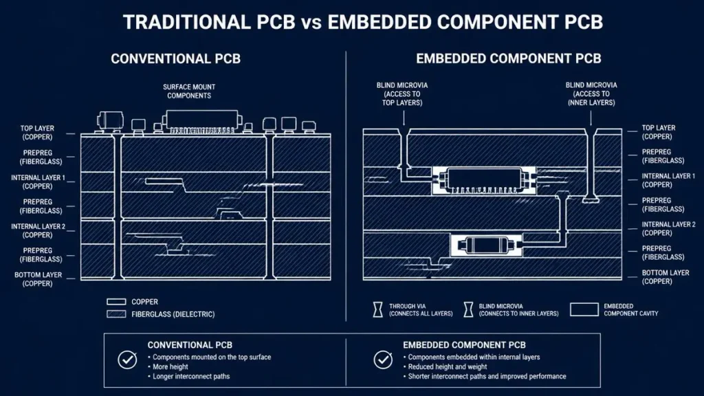
Conventional PCB vs Embedded Component PCB Structural Cross-Section Comparison
Embedded Component PCB fabrication normally costs more because the manufacturer must control additional variables such as component integration, cavity geometry, internal registration, lamination, buried interconnections, inspection, and yield.
A conventional multilayer PCB quotation generally revolves around:
Material → imaging → etching → lamination → drilling → plating → surface finish → testing
An embedded structure introduces additional cost exposure:
Component → cavity → placement → fixation → lamination → registration → interconnection → hidden inspection
The cost increase therefore comes from additional manufacturing constraints, not simply from the fact that a component is located inside the board.
For example, embedding a small passive resistor is not economically equivalent to embedding a bare semiconductor die.
The second structure may require:
- tighter placement control
- finer interconnection
- additional thermal analysis
- additional inspection
- more complex lamination
- more stringent reliability validation
This is why the phrase “embedded PCB cost” describes a family of cost structures rather than one fixed price.
What Are the Main Embedded Component PCB Cost Drivers?
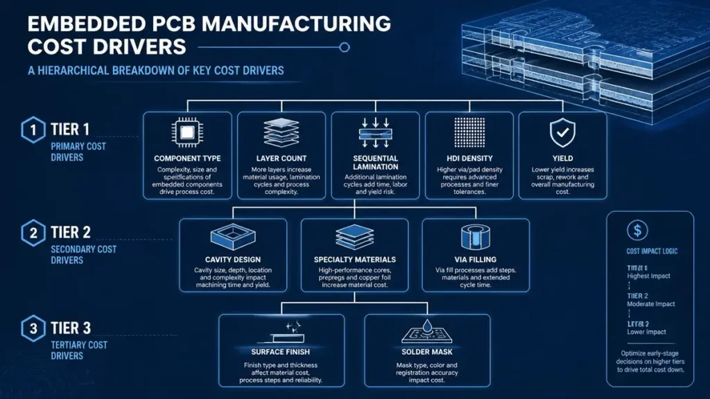
Embedded PCB Manufacturing Cost Drivers Hierarchical Breakdown
The most important cost drivers are embedded component type, layer count, sequential lamination, cavity complexity, microvia density, material selection, inspection requirements, production yield, and order volume.
A practical cost‑impact hierarchy is:
Tier 1 — Major cost drivers
- Embedded component type
- Layer count
- Sequential lamination
- HDI/microvia density
- Yield
- Production quantity
Tier 2 — Significant cost drivers
- Cavity count
- Cavity depth
- Cavity tolerance
- Copper thickness
- Via filling
- Specialty laminate
- Inspection method
Tier 3 — Secondary variables
- Surface finish
- Solder mask requirements
- Silkscreen
- Minor mechanical features
- Packaging
The important engineering point is that these variables interact.
For example:
Increasing layer count may increase cost.
But:
Increasing layer count while also increasing sequential lamination and microvia density can create a much larger cost increase.
Likewise:
A tighter cavity tolerance may appear to be a small specification change.
But if it reduces the process window enough to increase inspection and scrap, the commercial impact can be much larger.
How Does Layer Count Affect Embedded Component PCB Cost?
Higher layer counts generally increase material, lamination, imaging, drilling, plating, registration, and inspection costs, but the relationship is not strictly linear because sequential build‑up complexity can become a stronger cost driver than the number of copper layers alone.
Consider two hypothetical designs.
Design A
8‑layer multilayer PCB
- Single primary lamination route
- Moderate routing density
- Limited blind‑via requirements
- Four embedded passive components
Design B
12‑layer HDI PCB
- Sequential build‑up
- Multiple laser‑drilled microvia layers
- Via‑in‑pad
- Copper‑filled vias
- Higher registration requirements
- Sixteen embedded components
Design B has only four additional layers.
However, its manufacturing route is significantly more complicated.
That means procurement should avoid using:
Cost per PCB layer
as the only comparison metric.
A better metric is:
Cost per manufacturing process route.
Engineering cost question
Before removing a layer, check whether the change requires:
- more stacked microvias
- smaller pads
- tighter line/space
- additional lamination
- more difficult impedance control
Sometimes a slightly thicker stack‑up can actually produce a more economical production process.
How Does Sequential Lamination Increase Embedded PCB Pricing?
Sequential lamination increases cost because each additional build‑up cycle adds material handling, pressing, registration, drilling, plating, inspection, and yield exposure.
A simplified advanced build‑up route may look like:
Core fabrication
↓
Dielectric build‑up
↓
Laser drilling
↓
Desmear
↓
Copper deposition
↓
Electroplating
↓
Additional dielectric build‑up
↓
Laser drilling
↓
Plating
↓
Final outer‑layer processing
Every additional cycle introduces another opportunity for dimensional movement.
This matters particularly when an embedded component has already been positioned inside the internal structure.
Manufacturing pain point: cumulative registration
Suppose a hypothetical process has an individual registration variation of:
±25 µm
That number cannot simply be considered in isolation.
The final position may also be influenced by:
- component dimensional tolerance
- cavity tolerance
- laminate movement
- resin flow
- thermal expansion
- drilling registration
- copper distribution
The practical engineering requirement is therefore to manage the complete tolerance stack, rather than looking only at the nominal laser‑machine accuracy.
How Does Cavity Design Affect Embedded Component PCB Cost?
Cavity cost is influenced by cavity quantity, dimensions, depth, tolerance, geometry, component clearance, machining method, and inspection requirements.
A cost‑efficient cavity design usually has:
- standardized dimensions
- repeatable geometry
- reasonable clearance
- realistic depth tolerance
- minimal unique cavity families
A difficult design might contain:
- 20+ cavities
- several different depths
- narrow component‑to‑wall clearance
- irregular geometries
- tight dimensional tolerances
The number of cavities matters, but cavity diversity can matter almost as much.
Example
| Parameter | Cost‑optimized concept | High‑complexity concept |
|---|---|---|
| Cavity count | 4 | 20 |
| Cavity depth | 300 µm | 300–800 µm |
| Depth tolerance | ±50 µm | ±20 µm |
| Cavity families | 1–2 | 5–6 |
| Component clearance | 150 µm | 50 µm |
| Inspection | Sampling | Expanded inspection |
The second design creates a narrower manufacturing window.
That can increase:
engineering time + tooling + inspection + scrap exposure.
Engineering experience
One of the most common cost mistakes is specifying a cavity tolerance from a CAD perspective rather than from the component’s actual functional requirement.
If the component operates reliably with a larger dimensional window, forcing a significantly tighter tolerance may add manufacturing cost without adding product value.
How Do Embedded Component Tolerances Affect Cost?
Tighter component placement, cavity, dielectric, and interconnection tolerances generally increase process‑control and inspection requirements.
The final embedded structure is governed by a tolerance stack:
Ttotal = f(Tcomponent, Tcavity, Tplacement, Tlamination, Tvia)
For example, if:
- Component positional tolerance = ±30 µm
- Cavity registration = ±25 µm
- Lamination movement = ±35 µm
the manufacturer must evaluate their combined effect rather than assuming that each individual specification is independent.
This becomes increasingly important when:
- component clearance is small
- via pads are small
- microvias are stacked
- fine‑line routing is used
Cost optimization principle
Do not ask:
“What is the smallest tolerance you can manufacture?”
Ask:
“What tolerance does the product actually require?”
That question can produce meaningful cost reductions.
How Do Microvias and HDI Increase Embedded Component PCB Cost?
Microvias increase cost through laser drilling, desmear, copper deposition, electroplating, filling, registration control, inspection, and reliability verification.
Typical advanced interconnect structures include:
- Blind microvias
- Staggered microvias
- Stacked microvias
- Via‑in‑pad
- Copper‑filled vias
- Any‑Layer HDI
The manufacturing burden increases as the design moves toward greater via density and tighter geometry.
Example
Imagine two otherwise similar boards:
Board A
- 400 microvias
- Mainly staggered structures
- Limited via‑in‑pad
Board B
- 1,500 microvias
- Stacked microvias
- Via‑in‑pad
- Copper‑filled structures
Board B can have a substantially higher manufacturing cost despite having:
- identical board dimensions
- identical layer count
- identical base laminate
The difference comes from interconnect density and process complexity.
The hidden cost
Microvias also introduce reliability exposure.
A defective surface connection may be relatively easy to detect.
A buried microvia defect can remain hidden until:
- electrical test
- thermal cycling
- cross‑section
- reliability testing
- field operation
Therefore:
microvia density affects both fabrication cost and quality‑control cost.
How Does mSAP Affect Embedded Component PCB Cost?
mSAP can increase fabrication complexity, but it becomes economically justified when fine‑line requirements exceed the practical capability of conventional subtractive etching.
The relevant question is not:
“Is mSAP more advanced?”
It is:
“Does this design require mSAP?”
For an advanced embedded PCB, mSAP can support:
- fine‑line routing
- high‑density escape
- substrate‑like structures
- fine‑pitch interconnections
- dense HDI architecture
Hongda’s published manufacturing information identifies 8/8 µm‑class mSAP capability for advanced fine‑line applications.
However, a procurement team should ask for the complete capability envelope:
- What line/space is qualified in production?
- What copper thickness is associated with that geometry?
- What registration tolerance is maintained?
- What production yield is achieved?
- Can cross‑section evidence be provided?
- Can the same process be transferred from prototype to volume production?
The cost of mSAP should therefore be evaluated against the routing problem it solves.
How Do PCB Materials Affect Embedded Component PCB Cost?
Material selection can materially affect embedded PCB pricing, especially when high‑Tg, low‑loss, low‑CTE, specialty dielectric, or high‑frequency materials are required.
Common material decisions include:
- Standard FR‑4
- High‑Tg FR‑4
- Low‑loss laminate
- Very‑low‑loss laminate
- Specialty dielectric
- Embedded resistor material
- High‑conductivity copper
- Low‑profile copper foil
For high‑speed designs, dielectric Dk/Df and copper surface characteristics can affect signal integrity and therefore the stack‑up architecture.
For example, Panasonic publishes representative MEGTRON7 values such as Tg around 200°C, Dk 3.31 at 14 GHz, and Df 0.0023 at 14 GHz for specified material variants. These are manufacturer‑specific values under stated test conditions and should not be treated as universal finished‑board properties.
Material cost optimization
Instead of automatically specifying premium laminate throughout the stack‑up, engineers can evaluate:
Critical high‑speed layers → low‑loss material
Non‑critical power/control layers → qualified lower‑cost material
A hybrid material strategy can sometimes reduce material cost while preserving electrical requirements.
However, material substitution must be validated for:
- Dk/Df
- CTE
- Tg
- Td
- lamination behavior
- dielectric thickness
- impedance
- reliability
A cheaper laminate that changes the stack‑up process or reliability profile is not necessarily a cheaper PCB.
How Do Embedded Components Change Material Consumption?
Embedded components can increase material and process requirements because the PCB must accommodate the component volume, cavity, dielectric structure, and lamination conditions.
The component itself occupies physical volume.
The manufacturer must then manage:
Component Z‑height + cavity depth + dielectric thickness + copper distribution + resin flow
This becomes especially important when multiple component heights exist on the same internal layer.
Manufacturing pain point: resin flow
During lamination, resin must flow around internal structures without creating unacceptable:
- voids
- resin starvation
- local dielectric variation
- mechanical stress concentration
Therefore, component placement and prepreg selection cannot be considered separately.
This is one reason an embedded PCB that looks straightforward in CAD can become difficult during actual lamination.
How Does Production Yield Change the Real Embedded PCB Cost?
Yield can have a greater financial impact than a small unit‑price difference because every rejected embedded board may contain already‑consumed material, components, processing time, and inspection resources.
Required Input = Required Good Units / Yield
Suppose procurement requires:
10,000 good boards
At 98% yield: 10,000 / 0.98 = 10,204
At 90% yield: 10,000 / 0.90 = 11,111
The difference is:
907 additional boards.
The financial impact includes more than PCB laminate.
It may include:
- embedded components
- copper
- prepreg
- lamination capacity
- laser processing
- plating
- inspection
- electrical testing
- labor
Why yield matters more for embedded structures
A conventional PCB defect may sometimes be repaired.
An internal embedded‑component defect can be much harder or impossible to repair economically.
Effective Cost = Quoted Cost / Yield
is a useful preliminary comparison.
It is not a complete TCO calculation, but it is a much better starting point than comparing nominal piece prices.
How Do NRE and Tooling Affect Embedded PCB Prototype Cost?
NRE and tooling can make prototype unit prices appear disproportionately high because engineering and setup costs are distributed across a small quantity.
A simplified formula is:
Unit Cost = Variable Cost + (NRE + Tooling) / Quantity
For example, if:
NRE + tooling = US$3,000
| Quantity | NRE + tooling allocation |
|---|---|
| 10 boards | US$300/board |
| 100 boards | US$30/board |
| 1,000 boards | US$3/board |
| 10,000 boards | US$0.30/board |
The exact commercial structure varies by supplier.
But the economic principle is universal:
Prototype cost and mass‑production cost should be evaluated separately.
A prototype quotation should therefore show:
- engineering/NRE
- tooling
- recurring PCB cost
- embedded components
- inspection
- testing
rather than presenting everything as one unexplained unit price.
How Does Production Volume Reduce Embedded PCB Unit Cost?
Higher production volume generally reduces the per‑unit impact of NRE, tooling, setup, engineering, and process preparation while improving purchasing efficiency for materials and components.
Consider a simplified example:
Prototype
20 pieces
High:
- engineering cost per board
- tooling allocation
- setup cost
- inspection cost
Pilot
500 pieces
Lower:
- NRE allocation
- setup cost per board
- component purchasing cost
Production
50,000 pieces
Potentially lower:
- material cost per unit
- component purchasing cost
- tooling allocation
- setup allocation
But volume alone does not guarantee a lower effective cost.
If yield deteriorates during volume production, the expected savings can disappear.
Therefore the commercial equation becomes:
Volume Cost = Unit Manufacturing Cost + Yield Loss + Logistics + Quality Cost
How Does Panel Utilization Affect Embedded PCB Pricing?
Better panel utilization can reduce the effective material and processing cost allocated to each board, particularly for small and medium‑size embedded PCBs.
Consider a simplified example.
Panel A
8 boards/panel
Optimized Panel B
12 boards/panel
The second layout provides: (12‑8)/8 × 100% = 50% more boards per panel.
That does not mean the PCB automatically becomes 50% cheaper.
Panel utilization also depends on:
- tooling rails
- coupons
- copper balance
- cavity location
- routing
- V‑scoring
- board orientation
- component placement
- electrical test requirements
An experienced CAM/DFM engineer should therefore evaluate panelization before the quotation is finalized.
What Manufacturing Problems Create Hidden Embedded PCB Costs?
The most expensive hidden costs usually come from defects that appear late in the manufacturing cycle, because the board has already accumulated material, component, lamination, HDI, plating, and inspection costs.
1. Component‑to‑cavity misregistration
A component can be correctly placed according to the placement program but become misaligned relative to subsequent PCB features.
Potential consequences:
rework → rejection → scrap
2. Lamination movement
Thermal and mechanical changes can alter the final position of internal structures.
Potential consequences:
via misregistration → electrical defect → scrap
3. Resin voids
Voids around embedded structures can create:
- mechanical weakness
- thermal resistance
- reliability risk
4. Microvia interface failure
Potential causes include:
- poor copper interface
- insufficient plating
- unfavorable geometry
- thermal/mechanical stress
5. Cavity dimensional drift
If cavity dimensions move outside the functional window, component fit and lamination behavior can be affected.
6. Hidden internal defects
Surface AOI cannot reveal every internal defect.
Therefore advanced inspection may include:
- 3D AOI
- X‑ray
- electrical testing
- cross‑section analysis
Hongda’s published pillar material specifically identifies AOI, 3D inspection, X‑ray, cross‑section analysis and electrical testing as important controls for hidden embedded structures.
How Does Inspection Affect Embedded Component PCB Cost?
Inspection adds direct cost, but insufficient inspection can create a much larger downstream cost when internal defects are discovered after assembly or qualification.
A risk‑based inspection architecture can include:
Prototype
- X‑ray
- 3D inspection
- electrical test
- selected cross‑sections
Pilot production
- increased X‑ray sampling
- process coupons
- electrical test
- dimensional verification
Mass production
- AOI
- electrical test
- risk‑based X‑ray
- statistical process monitoring
- periodic cross‑section
The correct inspection level depends on:
- component type
- application criticality
- defect consequences
- customer quality requirements
- qualification requirements
The objective should not be:
Maximum inspection at maximum cost.
It should be:
Sufficient inspection to control the actual failure modes.
How Can Engineers Reduce Embedded Component PCB Cost Without Sacrificing Reliability?
The most effective cost reductions usually come from eliminating unnecessary process complexity before tooling rather than reducing material quality or inspection after production begins.
Cost optimization 1: Standardize cavities
Use common cavity dimensions wherever the component package permits.
Cost optimization 2: Reduce unnecessary microvias
Review whether every microvia is required electrically.
Cost optimization 3: Replace unnecessary stacked vias
Where routing permits, evaluate staggered structures.
Cost optimization 4: Optimize tolerances
Specify functional tolerances instead of automatically choosing the tightest possible tolerance.
Cost optimization 5: Reduce sequential lamination
A simpler build‑up route can improve:
- cycle time
- registration
- yield
- process stability
Cost optimization 6: Improve panel utilization
More usable boards per production panel can lower allocated process cost.
Cost optimization 7: Rationalize materials
Use specialty laminate where electrical or reliability requirements actually demand it.
Cost optimization 8: Control component sourcing
Use approved component alternatives where the design permits them.
Component shortages can otherwise become a hidden manufacturing cost.
How Does DFM Reduce Embedded Component PCB Cost?
DFM reduces cost by identifying high‑risk or unnecessary features before material purchasing, tooling, and production release.
A useful DFM review should connect five areas:
Electrical
- impedance
- signal loss
- current
- power integrity
Mechanical
- cavity dimensions
- component clearance
- board thickness
- warpage
Manufacturing
- line/space
- microvias
- sequential lamination
- copper thickness
- panelization
Inspection
- X‑ray
- AOI
- electrical testing
- cross‑section
Reliability
- CTE
- thermal cycling
- microvia reliability
- component stress
The important lesson is:
An electrically correct design is not automatically a cost‑optimized manufacturing design.
The pillar page already establishes DFM as a key part of Embedded Component PCB development.
This cost‑focused page should go one step further by showing how DFM decisions translate into dollars, yield, and production risk.
How Should Procurement Calculate Embedded Component PCB Total Cost of Ownership?
Procurement should compare suppliers using total cost of ownership rather than nominal PCB unit price.
TCO = PCB + Embedded Components + NRE + Tooling + Testing + Scrap + Logistics + Engineering
Then divide by the number of accepted units:
TCOgood = TCO / Accepted Units
Example supplier comparison
Assume:
Supplier A
- quoted PCB price: US$60
- yield assumption: 92%
Supplier B
- quoted PCB price: US$64
- yield assumption: 98%
For 5,000 accepted boards:
Supplier A requires approximately: 5,000 / 0.92 = 5,435
Supplier B requires approximately: 5,000 / 0.98 = 5,102
At nominal PCB pricing:
Supplier A ≈ US$326,100
Supplier B ≈ US$326,528
The apparent US$4/unit price difference almost disappears after yield is considered.
This example does not prove that one supplier is better. It demonstrates why procurement should ask for:
yield + scrap + testing + NRE + tooling + lead time + engineering support
before making a sourcing decision.
How Should Buyers Compare Embedded Component PCB Suppliers?
Buyers should compare suppliers based on manufacturing capability, process evidence, DFM quality, yield transparency, inspection capability, prototype‑to‑volume transfer, and total cost—not simply the lowest quotation.
Use this supplier evaluation matrix:
| Evaluation item | What procurement should verify |
|---|---|
| Embedded passive capability | Actual production examples |
| Embedded active capability | Qualified process range |
| Cavity capability | Dimensions + tolerance |
| Laser drilling | UV/CO₂ capability |
| Microvias | Stacked/staggered |
| Via filling | Process + inspection |
| Fine‑line | Production‑qualified geometry |
| mSAP | Actual line/space + copper |
| Lamination | Sequential build‑up capability |
| Inspection | AOI + X‑ray + electrical test |
| Yield | Similar‑project data |
| Prototype | Engineering support |
| Volume | Stable process transfer |
| Traceability | Lot/process records |
| Engineering | DFM before release |
| TCO | Transparent cost structure |
The pillar page already establishes these supplier‑evaluation criteria.
The cost page should not repeat that entire supplier‑selection discussion. Instead, it should answer the commercial question:
How does each supplier capability affect the final cost and production risk?
What Should an Embedded Component PCB RFQ Include?
A cost‑accurate RFQ should include the PCB manufacturing files, embedded component information, cavity specifications, stack‑up, quantity, material, interconnection requirements, inspection requirements, and application environment.
Minimum RFQ package
| RFQ information | Why it matters for cost |
|---|---|
| Gerber / ODB++ | Determines fabrication complexity |
| BOM | Determines component cost |
| Component manufacturer PN | Determines sourcing |
| Component dimensions | Determines cavity requirements |
| Component Z‑height | Determines stack‑up |
| Cavity drawing | Determines machining/laser work |
| Stack‑up | Determines material + lamination |
| Layer count | Determines fabrication route |
| Copper thickness | Determines plating/material |
| Via structure | Determines HDI complexity |
| Surface finish | Determines finishing cost |
| Quantity | Determines NRE allocation |
| Annual volume | Determines production economics |
| Testing | Determines inspection cost |
| Reliability requirement | Determines qualification cost |
The pillar page already specifies Gerber/ODB++, BOM, stack‑up, component specifications, quantity, application, reliability and testing as the core RFQ information.
For this cost‑focused page, the key addition is to explain why each item changes the quotation.
Which Embedded Component PCB Design Changes Usually Reduce Cost the Most?
The highest‑value design changes are usually those that reduce process cycles, microvia complexity, cavity diversity, material cost, or yield risk while preserving the required electrical and mechanical performance.
A practical optimization sequence is:
1. Review the component
Can the package be standardized?
2. Review the cavity
Can multiple cavity dimensions be consolidated?
3. Review the stack‑up
Can a lamination cycle be eliminated?
4. Review the vias
Can stacked microvias be reduced?
5. Review the material
Does every layer require the premium laminate?
6. Review the panel
Can board utilization be improved?
7. Review inspection
Which hidden features genuinely require enhanced inspection?
8. Review yield
Where is the likely process bottleneck?
This order is important.
If procurement starts by asking the supplier to reduce laminate cost by 5%, but the design has an unnecessarily complicated cavity and microvia structure, the larger savings opportunity may be elsewhere.
How Does Embedded Component PCB Cost Change Across Real Application Scenarios?
The economically optimal embedded PCB architecture depends strongly on the product’s mechanical envelope, electrical requirements, thermal load, production volume, and reliability target.
Scenario 1 — Compact medical electronics
Suppose a device has a strict enclosure limit.
Embedding selected passive components can recover surface area for:
- connectors
- sensors
- processors
- shielding structures
The correct economic comparison is:
Embedded PCB Premium vs. Mechanical Size Reduction + Assembly Savings
A higher PCB unit price may therefore be acceptable if it eliminates an expensive mechanical redesign.
Scenario 2 — Automotive electronics
Automotive applications often combine:
- restricted board area
- temperature variation
- vibration
- long service life
- high reliability requirements
Here, the cost analysis should include:
PCB fabrication + qualification + yield + reliability + assembly + system packaging
rather than fabrication cost alone.
The pillar page already identifies automotive and EV electronics as important embedded‑PCB applications.
Scenario 3 — Industrial power electronics
For power applications, the embedded structure may involve:
- thick copper
- embedded copper structures
- thermal paths
- power components
- large current transitions
Würth Elektronik’s embedding technology portfolio illustrates that embedded PCB technology can extend beyond passive components into copper and semiconductor integration. This is important because the cost model becomes increasingly system‑level as the architecture becomes more integrated.
For power electronics, procurement should evaluate:
Electrical Performance + Thermal Performance + Assembly Reduction + Mechanical Integration
against the PCB premium.
Scenario 4 — High‑speed computing
For high‑speed hardware, cost can be driven by:
- low‑loss dielectric
- controlled impedance
- fine‑line routing
- microvia density
- copper roughness
- layer count
- inspection
Embedding selected components may reduce electrical path length, but the cost benefit must be demonstrated at system level.
The pillar page already discusses controlled impedance, dielectric Dk/Df, copper roughness, return path, crosstalk and insertion loss as critical high‑speed considerations.
The cost question here is:
Does the electrical benefit justify the additional manufacturing complexity?
What Are the Most Common Mistakes When Estimating Embedded PCB Cost?
The most common mistakes are estimating from board size alone, ignoring NRE, ignoring yield, overlooking component sourcing, assuming layer count is the only major driver, and comparing suppliers only by nominal unit price.
Mistake 1: “The board is small, so it should be cheap.”
Small boards can be expensive if they contain:
- dense HDI
- fine‑line routing
- many cavities
- stacked microvias
- embedded active components
Mistake 2: “Adding one layer will always increase cost significantly.”
Not necessarily.
A simpler stack‑up can sometimes be cheaper than a lower‑layer architecture requiring extreme via density.
Mistake 3: “The cheapest quote is the cheapest supplier.”
Not if yield is significantly lower.
Mistake 4: “Prototype price predicts mass‑production price.”
NRE and tooling allocation can distort prototype unit pricing.
Mistake 5: “Tighter tolerances are always better.”
Only if the product requires them.
Mistake 6: “Advanced technology automatically means better economics.”
mSAP, stacked microvias, advanced laser processing and premium materials should be used because they solve a defined engineering problem—not simply because they are newer.
How Does Shenzhen Hongda Circuit Technology Approach Embedded Component PCB Cost Optimization?
Shenzhen Hongda Circuit Technology Co., Ltd. approaches Embedded Component PCB cost as a combined DFM, process‑capability, yield, and manufacturing‑route optimization problem, rather than treating quotation as a standalone purchasing activity.
Hongda’s published embedded‑PCB information identifies capabilities including:
- LDI fine‑line imaging
- UV/CO₂ laser drilling
- picosecond/femtosecond laser processing
- mSAP
- HDI microvias
- automated plating
- AOI
- X‑ray inspection
- high‑density multilayer PCB manufacturing.
These technologies are relevant to cost because they influence the manufacturer’s available process windows.
For example:
LDI
→ fine‑line registration
UV/CO₂ laser
→ microvia formation
mSAP
→ fine‑line density
Automated plating
→ copper consistency
AOI / X‑ray
→ defect detection
Process traceability
→ manufacturing consistency
The engineering objective is not to maximize every technology.
It is to select the simplest qualified process route that satisfies the customer’s requirements.
Our engineering approach
Before final quotation, an experienced engineering review should ask:
- Can the cavity geometry be standardized?
- Can the via structure be simplified?
- Can a sequential lamination cycle be removed?
- Does every layer require specialty material?
- Is the specified tolerance functionally necessary?
- Can panel utilization be improved?
- Which feature is most likely to limit production yield?
These questions often create more meaningful cost reductions than simply negotiating the final unit price.
How Can Procurement Get a More Accurate Embedded Component PCB Quote?
Provide complete design data and ask the manufacturer to return both the quotation and the technical assumptions behind it.
A strong RFQ request should ask the supplier to identify:
- PCB fabrication cost
- Embedded component cost
- Cavity/tooling cost
- NRE
- Material assumptions
- HDI/microvia assumptions
- Inspection cost
- Reliability testing
- Prototype lead time
- Volume pricing
- Yield assumptions
- Recommended cost‑reduction opportunities
The ideal quotation should allow procurement to understand:
Why the board costs what it costs
rather than simply showing:
Unit Price=$X
That transparency is particularly important for advanced embedded structures because many cost drivers are hidden inside the manufacturing process.
FAQ for Procurement Buyers
How much does an Embedded Component PCB cost?
A preliminary budget can range from roughly US$30–150 per prototype board for simpler embedded‑passive designs to US$150–500+ for complex HDI, active‑component, embedded‑die, or specialty‑material designs. Final pricing depends on the complete fabrication data, quantity, components, materials, testing, tooling, and yield.
Why is an Embedded Component PCB more expensive than a standard PCB?
The additional cost normally comes from component integration, cavity processing, lamination, internal registration, HDI/microvias, plating, hidden‑structure inspection, reliability validation, and potentially lower initial production yield.
What information do I need to request an Embedded Component PCB quotation?
Provide Gerber or ODB++ files, BOM, component manufacturer part numbers, component dimensions and Z‑heights, cavity drawings, stack‑up, material requirements, copper thickness, via structure, surface finish, quantity, testing requirements, and reliability requirements.
How can I reduce Embedded Component PCB manufacturing cost?
Start with DFM before tooling. Standardize cavity dimensions, reduce unnecessary microvias, simplify sequential lamination, use specialty materials only where required, optimize functional tolerances, improve panel utilization, and model yield before selecting the final design.
How should I compare Embedded Component PCB manufacturers?
Compare effective cost per accepted board, not quotation price alone. Evaluate DFM capability, cavity and HDI capability, laser drilling, mSAP, plating, X‑ray inspection, yield, reliability validation, engineering support, prototype capability, production scalability, NRE, tooling, and lead time
Final Engineering Takeaway
The lowest Embedded Component PCB cost does not necessarily come from the lowest PCB quotation. It comes from the lowest predictable cost per qualified board after accounting for design complexity, manufacturing yield, tooling, testing, components, and production volume.
The practical cost equation is:
\(\boxed{ Embedded\ PCB\ Cost = Design\ Complexity+ Process\ Complexity+ Material+ Components+ Testing+ Yield+ Volume }\)
The best optimization strategy is therefore: Simplify the architecture ↓ Optimize cavities ↓ Reduce unnecessary HDI complexity ↓ Select materials according to actual requirements ↓ Improve panel utilization ↓ Validate yield ↓ Compare suppliers using TCO
For engineers, this approach prevents over‑specification. For procurement teams, it prevents misleading unit‑price comparisons. For manufacturers, it creates a more stable path from prototype to volume production.
For Shenzhen Hongda Circuit Technology Co., Ltd., the goal is to make that engineering decision before production starts—when changing a cavity, via structure, stack‑up, tolerance, or material is still inexpensive.
Request an Embedded Component PCB cost review with your Gerber/ODB++, BOM and stack‑up.
Shenzhen Hongda Circuit Technology Co., Ltd. Embedded Component PCB | HDI | mSAP | Laser Drilling | Advanced Multilayer PCB Email: pcb@pcbkr.com Website: www.pcbkr.com
About Author
David Chen https://www.linkedin.com/in/pcbcoming
David Chen boasts an extensive professional background in PCBA manufacturing, PCBA testing, and PCBA optimization, with specialized expertise in high-precision PCBA fault analysis and rigorous PCBA reliability testing. The author has worked with high-layer-count server PCB fabrication, ultra-low-loss backplane stackups, and thermo-mechanical reliability optimization for AI infrastructure projects involving 112G and 224G PAM4 architectures. Skilled in complex circuit design and cutting-edge advanced PCB manufacturing processes, he delivers solutions that elevate product durability and performance across industrial applications. His technical articles focusing on PCBA manufacturing workflows and testing methodologies are widely cited by industry peers, research institutions, and technical platforms, solidifying his reputation as a recognized technical authority in the global circuit board manufacturing sector.