Consumer Electronics Embedded Component PCB: Design, Manufacturing & Procurement Guide
Consumer electronics manufacturers are under constant pressure to put more functions into smaller products. Embedded Component PCB technology helps recover PCB surface area, shorten selected interconnects and increase functional density by integrating passive or active components inside the PCB structure. For smartphones, wearables, TWS earbuds, AR/VR devices and compact IoT products, however, successful implementation depends on much more than miniaturization: cavity tolerance, Z‑height, HDI registration, microvia reliability, thermal management, inspection and production yield must be engineered together.
Why Are Embedded Component PCBs Becoming Important in Consumer Electronics?
Embedded Component PCBs are increasingly valuable when conventional surface‑mounted components consume too much board area, routing becomes congested, or the product requires shorter electrical interconnects within a highly constrained mechanical envelope.
Consumer electronics has a unique PCB problem: More functionality + less available volume + higher electrical performance requirements.
A modern compact product may contain:
- Application processors
- PMICs
- Memory
- RF transceivers
- Sensors
- Cameras
- Audio circuits
- Wireless interfaces
- Battery‑management electronics
- USB and high‑speed interfaces
- Power‑conversion circuits
All of these compete for limited PCB area.
The PCB must also coexist with: battery + camera + antenna + shielding + speaker + connector + mechanical frame + thermal interface.
This means PCB area is no longer simply a layout parameter. It becomes a system‑level mechanical resource.
Embedded‑component technology changes the architecture by moving selected electronic functions from the outer PCB surface into internal layers or specially engineered cavities. The objective is not to embed as many components as possible. The objective is to determine:
Which components create the greatest system‑level benefit when they are moved inside the PCB?
That distinction is important.
IPC‑7092 specifically addresses the design and assembly implementation of embedded components, while IPC‑6012F includes active/passive embedded circuitry among the rigid‑board constructions covered by its qualification and performance framework.
For consumer electronics, embedding should therefore be considered as an architecture decision, not merely a PCB fabrication option.
Which Consumer Electronics Products Benefit Most From Embedded Components?
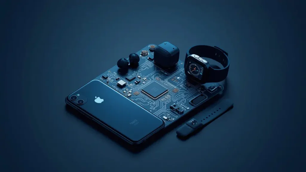
Applications of Embedded Component PCB in Consumer Electronics (Smartphones, Smartwatches & TWS Earbuds)
Smartphones, foldable devices, smartwatches, fitness trackers, TWS earbuds, AR/VR equipment, portable gaming products, compact cameras and miniature IoT devices are strong candidates because they combine high circuit density with severe mechanical constraints.
Smartphones
Smartphones have one of the strongest business cases for embedded PCB technology. The PCB must accommodate:
- High‑I/O processors
- Memory
- RF circuitry
- PMICs
- Camera interfaces
- High‑speed buses
- Antenna structures
- Shielding
- Battery connections
while occupying an extremely limited three‑dimensional volume.
An embedded capacitor or resistor network can potentially release surface area for:
- Fine‑pitch BGA escape routing
- RF structures
- Connectors
- Shielding
- Power components
- High‑speed interfaces
The advantage is therefore not simply: “smaller component.” It is: “more electronic functionality within the same product envelope.”
Smartwatches and Fitness Trackers
Wearables introduce an even more severe Z‑axis constraint. A small PCB may need to fit between: display + battery + enclosure + sensor + strap mechanism.
A design may therefore target PCB thickness in the approximate range of 0.3–0.8 mm, depending on construction, while simultaneously requiring HDI microvias and fine‑pitch packages.
These values should be treated as engineering targets rather than universal manufacturing limits. The actual process window depends on:
- Material system
- Layer count
- Copper thickness
- Board size
- Microvia structure
- Lamination construction
- Production volume
TWS Earbuds
TWS earbuds are particularly interesting because the available PCB area may be irregular rather than rectangular. The PCB must coexist with:
- Battery
- Speaker
- Microphone
- Antenna
- Charging contacts
- Sensors
- RF shielding
- Plastic enclosure
A component that occupies only a few square millimeters on the PCB can therefore create a significant mechanical constraint. Embedding selected passive components can free a routing channel or reduce the required board envelope.
AR/VR Devices
AR/VR products combine:
- High‑speed digital interfaces
- Multiple cameras
- Display interfaces
- Wireless communication
- Sensors
- Power management
- Processor packages
These products benefit from high‑density interconnect structures, but thermal management becomes increasingly important as processing power increases.
Portable Gaming Electronics
Portable gaming products introduce another combination: high power + high I/O density + battery limitation + thermal concentration + limited enclosure volume.
Embedded technology can be useful for selected power and signal functions, but the thermal consequences must be evaluated before components are buried inside the PCB.
Which Components Should Be Embedded in a Consumer Electronics PCB?
The best candidates are components whose integration provides a measurable benefit in board area, electrical path length, routing density or system packaging without creating disproportionate thermal, reliability or manufacturing risk.
| Component Type | Potential Benefit | Main Risk | Typical Application |
|---|---|---|---|
| Embedded resistor | Surface‑area reduction | Resistance tolerance | Termination, bias, filtering |
| Embedded capacitor | Local decoupling | Capacitance/voltage/process variation | Processor power delivery |
| Embedded inductor | Integration | Q factor, coupling, thermal behavior | RF/power circuits |
| Embedded passive network | Routing reduction | Process complexity | Compact modules |
| Embedded IC | High integration | Thermal/reliability | Advanced modules |
| Embedded die | Maximum density potential | Interconnection and yield | Miniature electronics |
Würth Elektronik describes multiple embedding approaches, including SOLDER.embedding, MICROVIA.embedding, FLIP‑CHIP.embedding and COPPER.embedding, illustrating that “embedded PCB” is not a single manufacturing technology. The appropriate method depends on the component and required electrical/mechanical architecture.
Embedded Resistors
Embedded resistors can eliminate selected surface‑mounted resistors. For a planar resistive structure, a simplified relationship is: R = Rs × L/W
where:
- R = resistance
- Rs = sheet resistance
- L = resistor length
- W = resistor width
This means resistance depends not only on the resistive material but also on manufactured geometry. Therefore: material tolerance + etching tolerance + geometry tolerance = final resistance tolerance.
This is particularly important for:
- impedance matching
- analog filters
- termination
- precision sensor circuits
Sierra Circuits similarly emphasizes resistance tolerance, material selection and geometry as important factors when implementing embedded resistors.
Embedded Capacitors
Embedded capacitors are attractive when the design requires local decoupling close to an IC. A simplified capacitor relationship is: C = εA/d
where:
- C = capacitance
- ε = dielectric permittivity
- A = electrode area
- d = dielectric separation
Reducing dielectric thickness or increasing electrode area increases capacitance density. But the engineering decision cannot stop at capacitance. Engineers should also evaluate:
- ESR
- ESL
- voltage rating
- dielectric loss
- temperature behavior
- DC‑bias behavior
- manufacturing tolerance
For high‑speed processors, the objective is often to reduce the impedance of the power‑distribution network over the relevant frequency range rather than simply maximize capacitance.
How Should Engineers Decide Whether a Component Is Worth Embedding?
Compare the surface‑area savings, electrical benefit and mechanical benefit against the additional fabrication complexity, inspection requirements and expected production‑yield impact.
A practical decision equation is: Embedding Value = Area Saved + Electrical Benefit + Packaging Benefit − Manufacturing Risk − Cost Penalty
For example, embedding one 0201‑class resistor may save little if it does not solve a routing or mechanical problem. But embedding a group of decoupling structures beneath or adjacent to a high‑I/O processor may:
- free multiple SMT locations
- reduce routing congestion
- shorten local power paths
- simplify surface assembly
- improve packaging density
The second case has a much stronger engineering justification.
Expert Engineering Principle
Do not embed a component because the technology can embed it. Embed it because the product architecture benefits from embedding it.
This distinction becomes increasingly important as manufacturing complexity increases.
How Should a Smartphone Embedded Component PCB Be Architected?
The design should begin with the complete mechanical envelope and Z‑height restrictions, then establish embedded‑component zones, stack‑up, HDI architecture, thermal paths and high‑speed routing before final component placement.
A practical design sequence is: Mechanical Envelope ↓ Battery / Camera / Shield Keep‑Out ↓ Embedded Component Zones ↓ Stack‑Up Definition ↓ HDI Architecture ↓ Power / RF / High‑Speed Routing ↓ Microvia Strategy ↓ DFM Review ↓ Prototype
This sequence is important because embedding should not be added to a completed conventional PCB as an afterthought. A late‑stage cavity can conflict with:
- BGA escape routing
- Power planes
- Ground planes
- Microvias
- Via‑in‑pad
- RF traces
- Shielding
- Lamination thickness
- Component clearance
The embedded component must therefore be treated as part of the stack‑up architecture from the beginning.
How Does Z‑Height Affect Consumer Electronics Embedded PCB Design?
Z‑height can become as important as X/Y dimensions because a 100–200 μm dimensional change can be mechanically significant inside a tightly packaged consumer product.
A useful first‑order calculation is: Available Z Clearance = Enclosure Clearance − PCB Thickness − Component Height − Tolerance Stack
Consider a simplified example. Suppose:
- enclosure clearance = 1.20 mm
- PCB thickness = 0.60 mm
- embedded component height = 0.35 mm
- accumulated tolerance = 0.10 mm
Then: Available margin = 1.20 − 0.60 − 0.35 − 0.10 = 0.15 mm
A nominal design may appear acceptable, but only 150 μm of mechanical margin remains. That margin may be consumed by:
- lamination thickness variation
- component tolerance
- enclosure tolerance
- local PCB warpage
This is why consumer‑electronics embedded PCB designs should include Z‑axis tolerance analysis, not simply X/Y cavity dimensions.
How Should Cavity Dimensions Be Toleranced?
Cavity clearance should be calculated from the complete tolerance chain rather than from the nominal component dimensions alone.
A simplified lateral tolerance model is: Required Clearance ≥ Component Tolerance + Placement Error + Cavity Tolerance + Lamination Movement + Measurement Uncertainty
Consider a hypothetical component: 2.00 × 1.20 mm
If the design provides only a very small clearance around the component, the process window can disappear quickly once all manufacturing variations are accumulated.
Manufacturing Pain Point: Component‑to‑Cavity Interference
If the component moves toward a cavity wall during lamination, possible consequences include:
- mechanical stress
- dielectric thinning
- resin‑flow restriction
- component displacement
- microvia clearance problems
Manufacturing Pain Point: Excessive Cavity Clearance
An oversized cavity is not automatically safer. It can create:
- excessive resin volume
- increased void risk
- local mechanical weakness
- uneven lamination behavior
- additional PCB real estate consumption
The correct engineering target is therefore:
Sufficient process clearance without creating unnecessary cavity volume.
How Do HDI and Any‑Layer HDI Enable Embedded Component Miniaturization?
HDI allows designers to use small laser‑formed microvias and build‑up structures around embedded components, reducing the routing area consumed by conventional through‑hole interconnections.
Modern consumer electronics frequently combines:
- Laser microvias
- Blind vias
- Buried vias
- Via‑in‑pad
- Stacked microvias
- Staggered microvias
- Sequential lamination
- Fine‑line routing
- Any‑Layer HDI
Sierra Circuits identifies laser microvias, blind/buried vias, fine lines, via‑in‑pad and sequential build‑up as key elements of HDI construction.
For a compact processor area, the advantage is substantial. A conventional through‑hole via may extend through multiple layers and consume routing area. A laser microvia can connect only the layers that require connection. This creates greater routing freedom around:
- CSPs
- BGAs
- embedded passives
- RF modules
- power‑management devices
What Role Does mSAP Play in Consumer Electronics Embedded PCB Manufacturing?
mSAP can enable finer conductor geometries than conventional subtractive processing, making it useful when consumer‑electronics layouts are limited by package pitch, routing density or PCB area.
A simplified mSAP sequence is: Thin Copper Seed → Photoresist → LDI Imaging → Pattern Plating → Resist Stripping → Flash Etching
The advantage is that the final conductor is built up rather than produced entirely by removing a thick starting copper layer.
For advanced consumer electronics, this can help support:
- fine‑pitch BGA routing
- narrow traces
- dense escape routing
- compact HDI structures
- substrate‑like PCB architectures
Hongda’s published manufacturing information includes fine‑line and mSAP processing for advanced applications. However, procurement teams should avoid evaluating mSAP only by its smallest advertised geometry. The important question is:
What line/space can the supplier repeatedly manufacture at the required copper thickness, panel size and production yield?
That is much more meaningful than a laboratory minimum.
Why Is Laser Drilling Important for Embedded Consumer Electronics PCBs?
Laser drilling enables small blind microvias that reduce the area required for vertical interconnections and allow dense build‑up structures around embedded components.
The microvia process can be simplified as: Laser Ablation → Target‑Pad Exposure → Desmear → Copper Deposition → Electroplating → Via Fill → Inspection
The laser diameter is only one parameter. A reliable microvia requires control of:
- dielectric thickness
- laser energy
- ablation profile
- target‑pad exposure
- desmear
- copper coverage
- plating thickness
- fill quality
- interface integrity
Expert Engineering Point
A perfectly drilled microvia can still become an unreliable interconnect if the downstream copper interface is defective.
Therefore, microvia reliability should be qualified as a complete process chain, not as a drilling specification alone.
How Do Embedded Components Affect Signal Integrity in Consumer Electronics?
Embedded components can shorten selected electrical paths and reduce some parasitic effects, but improved signal integrity is never guaranteed by embedding alone.
Signal integrity depends on:
- trace geometry
- dielectric Dk
- dielectric Df
- copper roughness
- reference‑plane geometry
- via transitions
- return‑path continuity
- component placement
- impedance control
A simplified high‑speed chain is: Component Placement → Interconnect Length → Parasitic L/C → Impedance Discontinuity → Reflection → Insertion / Return Loss → System Margin
Therefore, an embedded capacitor placed close to an IC power pin may be electrically valuable. But if the surrounding stack‑up creates poor return paths, the expected benefit can be reduced.
Sierra Circuits recommends impedance modeling and prototype verification such as TDR measurements for embedded‑component designs.
How Should Embedded Capacitors Be Positioned for High‑Speed Consumer Electronics?
Embedded capacitors should generally be positioned to minimize the electrical path between the capacitor and the device power‑distribution network while maintaining appropriate reference‑plane and manufacturing clearance.
The goal is not simply: “capacitor close to IC.” The real goal is: low‑inductance current path + stable reference plane + controlled geometry.
A useful layout strategy is: IC power pin ↓ short connection ↓ embedded capacitance ↓ low‑inductance return path ↓ power/ground structure
For high‑speed processors, designers may combine embedded capacitance with conventional SMT capacitors so that different structures address different frequency regions. Sierra Circuits similarly recommends placing embedded capacitors close to IC power pins and combining embedded and discrete capacitors where appropriate.
How Should Thermal Management Be Designed When Components Are Embedded?
Thermal management must be designed as a complete heat path because an embedded component can lose direct access to the external environment.
A simplified thermal relationship is: ΔT = P × θJA
where:
- ΔT = temperature rise
- P = dissipated power
- θJA = effective thermal resistance
For example, if a component dissipates: 0.50 W and the effective thermal resistance is: 30 °C/W the estimated temperature rise is: 0.50 × 30 = 15 °C
If the thermal architecture increases effective resistance to: 50 °C/W the temperature rise becomes: 25 °C
That additional 10 °C can be significant in a sealed wearable enclosure.
Thermal Design Options
Depending on the application, engineers may consider:
- Internal copper planes
- Thermal vias
- Copper heat spreaders
- Thermally conductive dielectric
- Metal stiffeners
- Graphite interfaces
- Thermal pads
- Enclosure conduction
The critical point is:
Do not embed a heat‑generating component before identifying where its heat will go.
Sierra’s embedded‑component guidance also highlights thermal vias, copper pours and thermal management as important considerations.
What Are the Most Difficult Manufacturing Problems in Consumer Electronics Embedded PCBs?
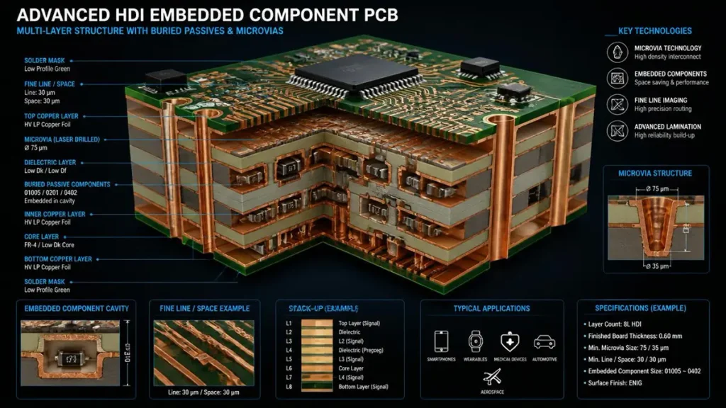
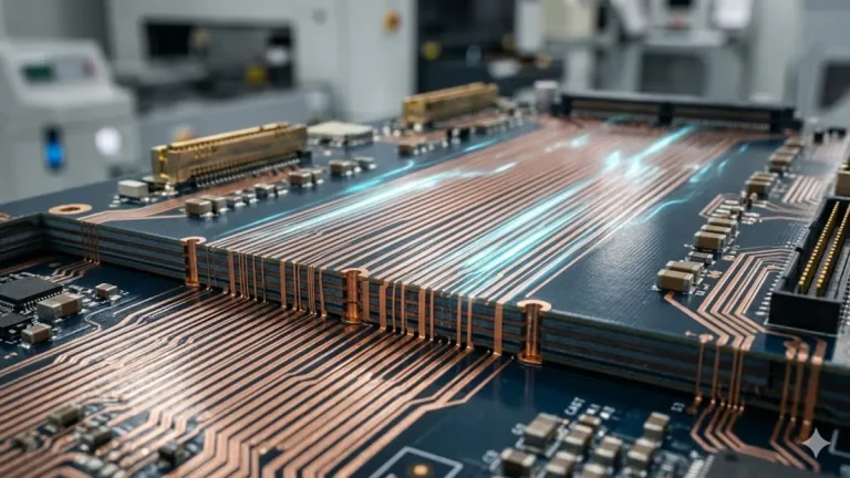
3D Cross-Section Diagram of Advanced HDI Embedded Component PCB Architecture
The most difficult problems are usually hidden defects and tolerance interactions involving component placement, cavity geometry, resin flow, lamination, microvias, copper plating, warpage and thermal cycling.
Manufacturing Pain Point 1: Component Movement During Lamination
A component may shift because of:
- thermal expansion
- pressure
- resin flow
- cavity geometry
- component restraint
The problem is not necessarily visible after fabrication. A small displacement may later create: component‑to‑via clearance failure or component‑to‑cavity‑wall interference.
Manufacturing Pain Point 2: Resin Voids
Voids can form around embedded components because of:
- trapped air
- insufficient resin flow
- unsuitable prepreg
- component‑edge geometry
- inadequate vacuum
- excessive cavity volume
A void may remain hidden inside the PCB and become difficult to detect through surface inspection.
Manufacturing Pain Point 3: Microvia Cracking
Potential causes include:
- excessive aspect ratio
- copper fatigue
- CTE mismatch
- poor plating
- stacked‑via stress
- repeated thermal cycling
This is why microvia reliability needs qualification rather than visual inspection alone. IPC‑6012F explicitly covers rigid‑board constructions that include microvias and active/passive embedded circuitry.
Manufacturing Pain Point 4: PCB Warpage
Thin consumer‑electronics PCBs are particularly sensitive to:
- copper imbalance
- asymmetric stack‑ups
- resin distribution
- laminate CTE
- thermal history
A board can pass electrical testing and still create problems during SMT if warpage causes:
- placement errors
- poor solder joints
- BGA opens
- connector misalignment
Manufacturing Pain Point 5: Hidden Delamination
Possible causes include:
- moisture
- contamination
- poor bonding
- CTE mismatch
- incorrect lamination profile
- excessive thermal exposure
Because the structure is buried, external visual inspection may not identify the defect.
Manufacturing Pain Point 6: Component‑to‑Via Collision
This is one of the most important tolerance‑chain problems. A cavity may be correctly located. The embedded component may also be correctly placed. But if the subsequent laser microvia shifts relative to the component, the finished structure can still fail.
Therefore:
The manufacturing datum strategy must connect cavity registration, component placement, imaging and laser drilling.
Simply tightening one individual tolerance does not solve a poorly coordinated tolerance chain.
How Should Thin Consumer Electronics PCBs Be Designed to Reduce Warpage?
Warpage should be addressed through balanced copper distribution, symmetrical stack‑up design, controlled dielectric construction and appropriate lamination parameters.
A simplified engineering model is: Warpage Risk ∝ CTE Mismatch + Copper Imbalance + Stack‑Up Asymmetry + Thermal Stress
Therefore, the designer should review:
- copper percentage by layer
- dielectric thickness
- core symmetry
- prepreg distribution
- plane distribution
- embedded‑component locations
For example, placing a large copper power plane on one side while leaving the corresponding region on the opposite side largely empty can increase local mechanical imbalance.
This is particularly important for:
- smartwatches
- smartphones
- TWS earbuds
- rigid‑flex assemblies
- ultra‑thin HDI boards
How Should TWS Earbud PCBs Be Engineered Around Mechanical Constraints?
TWS earbud PCBs should be designed as three‑dimensional mechanical systems rather than simply miniature versions of conventional rigid PCBs.
A typical conceptual architecture may involve: Battery ↓ Embedded Passive Region ↓ HDI Processor / RF Region ↓ Antenna Clearance ↓ Charging Interface
The designer must simultaneously control:
- PCB outline
- component Z‑height
- battery clearance
- speaker clearance
- antenna clearance
- flex transition
- charging contacts
- cavity geometry
Scenario Example
Suppose a TWS PCB has:
- 4–6 layers
- approximately 50–75 μm microvias
- approximately 35/35 μm routing
- 0201‑class external passives
- one embedded decoupling structure
The question should not be:
“Can all of these features be manufactured?”
The better question is:
Does embedding the component create enough system‑level benefit to justify the additional fabrication complexity?
If the embedded structure only eliminates one tiny SMT component, the economic justification may be weak. If it releases a routing channel or reduces the PCB outline enough to improve enclosure design, the business case becomes much stronger.
How Should Wearable PCBs Handle Embedded Components Near Batteries and Sensors?
Wearable embedded PCBs require careful separation between embedded components, battery structures, sensors, antennas and heat‑generating devices because the available mechanical and thermal margins are usually small.
For wearable products, review:
Battery Clearance
Avoid creating mechanical pressure points.
Sensor Clearance
Sensitive analog sensors should be isolated from:
- high‑current paths
- switching regulators
- high‑speed digital structures
RF Clearance
Maintain the required antenna and ground architecture.
Thermal Clearance
Keep heat‑generating components away from temperature‑sensitive sensors.
Z‑Height
Account for:
- PCB thickness
- component height
- cavity depth
- enclosure tolerance
- adhesive thickness
- thermal‑interface material
This creates a genuine system‑level PCB design problem, not merely a component‑placement problem.
How Should RF Performance Be Managed in Embedded Consumer Electronics PCBs?
RF performance depends on the entire electromagnetic architecture, including dielectric properties, trace geometry, grounding, copper roughness, return paths, shielding and embedded‑component placement.
Engineers should evaluate:
- Dk
- Df
- copper roughness
- trace width
- trace spacing
- ground‑plane continuity
- via transitions
- shielding
- antenna clearance
- component coupling
A lower‑loss material may improve insertion loss, but material selection alone does not guarantee RF performance. Similarly, embedding a passive component does not automatically improve RF performance. The complete RF structure must be simulated and measured.
How Does Embedded Component PCB Technology Compare With Conventional SMT?
SMT remains simpler, easier to repair and often cheaper for conventional products, while embedded components become attractive when board area, routing density, electrical path length or packaging volume becomes the dominant constraint.
| Parameter | Embedded Component PCB | Conventional SMT PCB |
|---|---|---|
| Component location | Internal + surface | Mainly surface |
| Surface‑area utilization | Very high | Moderate to high |
| Routing density | Very high potential | High |
| Manufacturing complexity | Higher | Lower |
| Inspection | More difficult | Easier |
| Repairability | Lower | Higher |
| DFM requirement | High | Moderate |
| Prototype cost | Usually higher | Usually lower |
| Miniaturization | Excellent potential | Good |
| Thermal analysis | More demanding | More straightforward |
| Hidden‑defect risk | Higher | Lower |
| Mass‑production qualification | More stringent | More standardized |
The decision should therefore be application‑driven. For a low‑cost controller with plenty of board space, SMT may be the better solution. For a miniature wearable where every square millimeter matters, embedded technology may justify its additional manufacturing complexity.
How Does mSAP Affect Consumer Electronics PCB Cost?
mSAP can increase fabrication complexity, but it can reduce total system cost when its fine‑line capability enables smaller boards, fewer layers, simpler package escape or fewer assembly operations.
A useful procurement model is: Total Cost = PCB Fabrication + Tooling + Yield Loss + Assembly Impact + Inspection + Logistics + Engineering
Therefore, comparing only: $/PCB can produce the wrong purchasing decision.
For example, an advanced mSAP board may have a higher bare‑board price but enable:
- smaller PCB dimensions
- fewer build‑up layers
- reduced component count
- simplified SMT
- improved package escape
- reduced product volume
The correct metric is: system‑level cost per finished product.
What Is the Difference Between Minimum Capability and Production Capability?
Minimum capability describes what a manufacturer can potentially produce under favorable conditions, while production capability describes what the supplier can repeatedly manufacture within a defined quality and yield window.
This distinction is critical. Suppose a supplier advertises: 8/8 μm line/space
The procurement team should ask:
- At what copper thickness?
- On what material?
- At what panel size?
- At what layer?
- At what registration tolerance?
- Prototype or production?
- What is the yield?
- What inspection method verifies the geometry?
- Is cross‑section evidence available?
Expert Procurement Rule
Never design a high‑volume product around a supplier’s absolute minimum geometry unless that geometry has been production‑qualified for the actual stack‑up and volume.
A slightly larger geometry with stable process margin can be commercially superior to an ultra‑fine geometry operating at the edge of the process window.
How Should Embedded Component PCBs Be Inspected?
Inspection should combine surface inspection, hidden‑structure inspection, dimensional verification, microsection analysis and electrical testing because no single method can verify every embedded feature.
| Inspection Method | Main Purpose |
|---|---|
| 2D/3D AOI | Surface defects |
| X‑ray / AXI | Buried components and interconnects |
| Dimensional inspection | Cavity and board geometry |
| Microsection | Internal construction |
| Electrical test | Opens and shorts |
| TDR | Impedance verification |
| Via‑chain coupon | Microvia reliability |
| Thermal cycling | Thermomechanical validation |
| Reflow simulation | Assembly thermal exposure |
Sierra Circuits’ consumer‑electronics manufacturing documentation similarly identifies DFM/DFA, thermal cycling, thermal shock, AOI, X‑ray, flying‑probe/ICT and documentation as relevant quality activities.
Expert Engineering Experience
For buried structures, functional electrical testing should not be the only acceptance gate. A board can pass an electrical test at room temperature while containing a structural defect that becomes significant after:
- thermal cycling
- repeated reflow
- mechanical stress
- humidity exposure
For development builds, a stronger sequence is: Prototype → X‑Ray → Microsection → Electrical Test → Thermal/Reflow Exposure → Re‑Test → Process Optimization → Pilot Run → Production Qualification
How Should Consumer Electronics OEMs Prepare an Embedded PCB RFQ?
An embedded PCB RFQ should describe the electrical, mechanical, material, embedded‑component, inspection and reliability requirements in enough detail for the manufacturer to evaluate the complete construction.
PCB Manufacturing Data
Provide:
- Gerber or ODB++
- IPC‑2581 where applicable
- fabrication drawing
- stack‑up
- drill files
- embedded‑component layers
- cavity drawings
- impedance requirements
Component Data
For each embedded component:
- manufacturer
- part number
- package
- X/Y dimensions
- Z‑height
- terminal dimensions
- operating temperature
- moisture sensitivity
- electrical requirements
Manufacturing Requirements
Specify:
- layer count
- finished thickness
- copper thickness
- minimum line/space
- microvia diameter
- via structure
- cavity dimensions
- cavity tolerance
- registration
- surface finish
- material family
Quality Requirements
Specify:
- X‑ray requirements
- microsection requirements
- electrical testing
- thermal cycling
- reflow exposure
- reliability standards
- acceptance criteria
Commercial Requirements
Include:
- prototype quantity
- pilot quantity
- annual volume
- target lead time
- packaging
- approved component sources
For extremely compact products, provide a 3D mechanical envelope whenever possible. A Gerber file alone cannot show every mechanical interference problem.
How Should Procurement Teams Qualify an Embedded Component PCB Manufacturer?
Supplier qualification should be based on demonstrated manufacturing evidence rather than a generic capability list.
Use this supplier scorecard:
| Qualification | Evidence to Request |
|---|---|
| Embedded component experience | Comparable production examples |
| Cavity capability | Dimensional inspection |
| Component placement | Registration data |
| Lamination | Process qualification |
| HDI | Cross‑section samples |
| Microvias | Via reliability evidence |
| mSAP | Qualified production geometry |
| Laser | Via diameter and positional data |
| X‑ray | Hidden‑structure inspection |
| AOI | Inspection capability |
| Electrical test | Test coverage |
| DFM | Formal engineering review |
| Yield | Pilot/production data |
| Traceability | Lot/process records |
| Volume transfer | Prototype‑to‑production plan |
The Most Important Question
Do not ask only:
“Can you manufacture this PCB?”
Ask:
“What production yield do you normally achieve for structures comparable to ours?”
That question separates laboratory capability from manufacturing capability.
What Are the Most Common Consumer Electronics Embedded PCB Design Mistakes?
The most common mistakes are adding embedded components too late, designing around absolute minimum geometries, ignoring Z‑height, underestimating tolerance accumulation and failing to validate hidden structures.
Mistake 1: Embedding Components After Layout Completion
This often causes conflicts with:
- vias
- planes
- traces
- cavities
- BGA escape
- shielding
Mistake 2: Designing to the Supplier’s Absolute Minimum
Minimum geometry should not automatically become the production target.
Mistake 3: Ignoring Z‑Height
Consumer electronics is three‑dimensional.
Mistake 4: No Tolerance Stack
Nominal CAD dimensions are not manufacturing dimensions.
Mistake 5: No Thermal Path
A buried heat source still has to dissipate heat.
Mistake 6: No Hidden‑Structure Inspection Plan
If a component is buried, define how it will be inspected before production.
Mistake 7: Prototype and Production Use Different Processes
If the prototype uses one material or lamination system and mass production uses another, the prototype may not adequately represent production reliability.
How Should Consumer Electronics Embedded PCBs Be Transferred From Prototype to Mass Production?
The prototype‑to‑production process should freeze the material system, component source, cavity structure, lamination process, microvia architecture, inspection criteria and acceptance requirements before volume release.
A robust transfer sequence is: Engineering Prototype ↓ Cross‑Section Validation ↓ Electrical Validation ↓ Thermal/Reflow Reliability ↓ Process Optimization ↓ Pilot Run ↓ First‑Pass Yield Review ↓ Process Freeze ↓ Mass Production
What Should Be Frozen?
At minimum:
- PCB material
- copper foil
- stack‑up
- cavity geometry
- embedded component source
- placement method
- lamination process
- laser process
- via‑fill process
- surface finish
- inspection criteria
- electrical testing
- packaging
The objective is process equivalence, not merely dimensional similarity.
What PCB Manufacturing Technologies Matter Most for Consumer Electronics?
The most relevant technologies include Any‑Layer HDI, advanced mSAP, finer laser microvias, low‑loss materials, rigid‑flex integration, automated X‑ray/3D inspection and increasingly data‑driven process control.
Any‑Layer HDI
Useful for:
- processor escape
- memory
- RF
- high‑speed interfaces
- embedded passive regions
Advanced mSAP
Useful when:
- package pitch is tight
- board area is restricted
- conventional etching limits routing density
Advanced Laser Processing
UV and CO₂ laser processes provide different process windows for microvia formation and dielectric ablation. Specialized ultrashort‑pulse laser processes may be considered for specific advanced structures. The appropriate laser depends on: material + dielectric thickness + via diameter + target pad + production volume.
Low‑Loss Materials
For high‑speed consumer electronics, engineers may evaluate:
- low‑Df laminates
- modified PPE/PPO systems
- hydrocarbon resin systems
- PTFE‑based materials
- low‑profile copper
Material selection should be based on measured electrical, thermal and mechanical performance rather than brand name alone.
Digital Process Control
Advanced manufacturing is increasingly incorporating:
- automated inspection
- process traceability
- digital production records
- SPC
- equipment data
- automated defect classification
The long‑term direction is: PCB fabrication + data + inspection + process feedback rather than isolated manufacturing operations.
How Can Engineers Reduce Embedded PCB Risk Before Prototyping?
The most effective strategy is to identify the highest‑risk dimensions and structures before tooling, then increase process margin wherever electrical performance allows.
Risk A — Minimum Geometry
Ask:
Does the design genuinely require the minimum supplier capability?
If not, increase the geometry.
Risk B — Cavity Clearance
Calculate: Available Clearance − Component Tolerance − Placement Tolerance − Cavity Tolerance − Lamination Movement
Risk C — Z‑Height
Calculate: Enclosure Clearance − PCB Thickness − Component Height − Tolerance
Risk D — Microvia Reliability
Check:
- diameter
- depth
- aspect ratio
- target pad
- copper thickness
- stacking
- thermal exposure
Risk E — Warpage
Review: Copper Balance + Stack‑Up Symmetry + Material CTE + Lamination History before manufacturing.
How Does Shenzhen Hongda Approach Consumer Electronics Embedded Component PCB Manufacturing?
Shenzhen Hongda Circuit Technology Co., Ltd. treats embedded‑component PCB manufacturing as an integrated engineering process covering DFM, cavity formation, component integration, lamination, HDI, laser microvias, fine‑line/mSAP, plating and inspection.
A representative process is: DFM Review ↓ Material Selection ↓ Inner‑Layer Circuit Formation ↓ Cavity Formation ↓ Component Placement ↓ Lamination ↓ Laser Microvia Formation ↓ Desmear ↓ Copper Deposition ↓ Electroplating ↓ Fine‑Line / mSAP Processing ↓ Outer‑Layer Formation ↓ Surface Finish ↓ AOI / 3D Inspection ↓ X‑Ray ↓ Electrical Test ↓ Final Inspection
The important engineering principle is that these processes cannot be optimized independently. For example: Cavity accuracy affects component position which affects microvia registration which affects electrical connectivity which ultimately affects yield and reliability.
Our Engineering Approach
When reviewing an embedded‑component design, we focus on the complete tolerance chain: Component Tolerance + Placement Tolerance + Cavity Tolerance + Lamination Movement + Laser Registration + Via Landing Tolerance =
Final Manufacturing Margin
This is particularly important for consumer electronics because the available mechanical margin is often extremely small.
How Can Shenzhen Hongda Support Consumer Electronics OEMs and ODMs?
Shenzhen Hongda Circuit Technology Co., Ltd. can support consumer‑electronics projects from engineering review and PCB fabrication through advanced HDI/mSAP structures, embedded‑component processing, inspection, prototyping and PCB assembly.
Relevant manufacturing technologies include:
- Embedded component PCB
- Embedded passive PCB
- HDI PCB
- Any‑Layer HDI
- mSAP PCB
- Fine‑line PCB
- Laser microvia PCB
- Rigid‑flex PCB
- High‑density multilayer PCB
- Low‑loss/high‑frequency PCB
- 3D AOI
- X‑ray inspection
- Electrical testing
- PCB assembly
For consumer electronics, our engineering review should focus on: Mechanical Envelope → Component Selection → Embedded Location → Cavity → Z‑Height → Stack‑Up → HDI → Microvia → Lamination → Thermal Path → Inspection → Assembly → Production Yield
The goal is not merely to determine whether a PCB can be fabricated. The goal is to determine whether it can be repeatedly manufactured at the required quality, reliability and commercial yield.
How Should Buyers Evaluate the Cost of an Embedded Consumer Electronics PCB?
Buyers should evaluate total manufacturing cost rather than bare‑board price because embedded structures introduce additional engineering, tooling, inspection and yield considerations.
The cost model should include: PCB Fabrication + Embedded Component Processing + Tooling + Material + Laser Processing + Inspection + Testing + Yield Loss + Assembly Impact + Logistics + Engineering Cost
For example, a lower unit quotation may become more expensive if the supplier produces:
- higher scrap
- more engineering changes
- more rework
- lower first‑pass yield
- longer lead times
Therefore:
The cheapest quotation is not necessarily the lowest total cost.
For consumer electronics, production yield can be more important than a small difference in nominal unit price.
How Can Embedded Components Solve Common Consumer Electronics Buyer Pain Points?
Embedded components can address board‑space limitations, routing congestion, high component density and selected electrical‑path problems, but each benefit must be balanced against manufacturing complexity.
Pain Point 1: The PCB Is Too Large
Potential Solution: Embed selected passive components to recover surface area.
Pain Point 2: Too Many Surface Components
Potential Solution: Move appropriate resistive or capacitive functions into internal PCB structures.
Pain Point 3: Routing Around Fine‑Pitch Packages Is Too Dense
Potential Solution: Combine embedded components with HDI, microvias and fine‑line routing.
Pain Point 4: Local Decoupling Paths Are Too Long
Potential Solution: Evaluate embedded capacitance close to the relevant power‑distribution structure.
Pain Point 5: The Product Has Severe Z‑Height Constraints
Potential Solution: Use internal component integration to reduce surface‑mounted component height.
Pain Point 6: Prototype Works but Mass Production Is Unstable
Potential Solution: Improve DFM, process qualification, inspection and production‑yield control before volume release.
What Should Procurement Teams Ask an Embedded Component PCB Supplier?
Buyers should ask questions that reveal actual production capability, not simply whether the supplier offers embedded PCB technology.
1. Can you provide comparable production examples?
Ask for evidence involving:
- similar component size
- similar cavity
- similar HDI
- similar layer count
- similar production volume
2. What is your qualified production line/space?
Ask for:
- copper thickness
- material
- panel size
- production yield
- cross‑section evidence
3. How do you inspect hidden embedded structures?
Ask whether the process includes:
- X‑ray
- microsection
- electrical test
- process coupons
4. How do you control component‑to‑cavity registration?
Ask for actual dimensional capability rather than a generic statement.
5. How do you transfer prototypes into mass production?
Ask for:
- pilot‑run procedure
- process freeze
- material control
- yield monitoring
- traceability
These questions reveal considerably more than:
“Do you manufacture embedded PCBs?”
What Should Be Included in a Consumer Electronics Embedded PCB RFQ?
A complete RFQ should define the electrical, mechanical, embedded‑component, material, manufacturing, reliability and commercial requirements.
Required Files
- Gerber
- ODB++
- IPC‑2581 where applicable
- fabrication drawing
- stack‑up
- drill files
- BOM
- embedded‑component definition
- cavity drawings
Component Information
- manufacturer
- part number
- package
- dimensions
- Z‑height
- terminal structure
- temperature rating
- electrical requirements
PCB Requirements
- layer count
- finished thickness
- copper thickness
- line/space
- microvia structure
- via fill
- surface finish
- impedance
- material
- cavity tolerance
Quality Requirements
- X‑ray
- AOI
- microsection
- electrical test
- thermal cycling
- reflow simulation
- reliability requirements
Commercial Information
- prototype quantity
- pilot quantity
- annual volume
- target lead time
- packaging
- approved component sources
The more complete the RFQ, the less likely the quotation will be based on incorrect assumptions.
What Is the Future of Consumer Electronics Embedded Component PCB Technology?
The future is moving from conventional surface assembly toward increasingly integrated three‑dimensional electronic structures combining embedded components, HDI, mSAP, substrate‑like PCB technologies and advanced packaging.
The technology evolution can be represented as: Conventional Multilayer PCB ↓ HDI ↓ Any‑Layer HDI ↓ Fine‑Line / mSAP ↓ Embedded Passive Components ↓ Embedded Active Components / Die ↓ Substrate‑Like PCB ↓ Advanced Electronic Packaging
Würth Elektronik’s embedding technology portfolio demonstrates how embedded devices can be implemented through several distinct manufacturing approaches, while its application material emphasizes miniaturization, reliability and reduced installation space.
The future is therefore not simply about: “more PCB layers.” It is about: more functions per unit volume.
At the same time, inspection and manufacturing data will become increasingly important. The factory of the future will combine:
- LDI
- laser processing
- automated plating
- AOI
- 3D inspection
- X‑ray
- electrical testing
- SPC
- traceability
- digital production records
The result is a transition from: PCB manufacturing toward: integrated electronic‑structure manufacturing.
What Should Engineers Remember Before Choosing Embedded Components for Consumer Electronics?
Embedded components should be selected only when the system‑level benefits justify the additional manufacturing complexity and when the design has enough process margin for reliable production.
The most important principles are:
- Design the embedded structure from the beginning.
- Treat Z‑height as a controlled engineering dimension.
- Calculate tolerance accumulation instead of relying on nominal CAD dimensions.
- Do not confuse minimum supplier capability with stable production capability.
- Use HDI and mSAP where they solve a real routing or packaging problem.
- Define the thermal path before embedding heat‑generating components.
- Validate hidden structures with X‑ray and microsection techniques where appropriate.
- Use reliability testing for structures exposed to thermal and mechanical stress.
- Evaluate production yield as part of supplier qualification.
- Compare total system cost rather than bare PCB price.
The ultimate KPI is not the smallest line width. It is:
Maximum product functionality per unit volume with predictable manufacturing yield and reliability.
Frequently Asked Questions for Consumer Electronics PCB Buyers
Can you manufacture embedded component PCBs for smartphones and wearable devices?
Yes, Shenzhen Hongda Circuit Technology Co., Ltd. supports embedded‑component PCB structures for compact electronics, subject to design review of the component package, cavity geometry, stack‑up, HDI structure and production requirements.
The appropriate manufacturing process depends on the component type and construction.
What line width and spacing can you manufacture for consumer electronics embedded PCBs?
The qualified production geometry depends on copper thickness, material, panel size, layer structure and required yield. Buyers should request a production‑qualified line/space rather than relying on an absolute minimum capability.
The correct specification is therefore: Geometry + Copper Thickness + Material + Registration + Yield.
How do you inspect components buried inside the PCB?
Buried structures can be inspected through X‑ray/AXI, dimensional inspection, microsection analysis, electrical testing and appropriate reliability testing. Surface AOI alone cannot verify every internal structure.
IPC‑6012F specifically includes active/passive embedded circuitry and complex rigid‑board constructions within its qualification and performance framework.
What files are required for an embedded component PCB quotation?
Buried structures can be inspected through X‑ray/AXI, dimensional inspection, microsection analysis, electrical testing and appropriate reliability testing. Surface AOI alone cannot verify every internal structure.
IPC‑6012F specifically includes active/passive embedded circuitry and complex rigid‑board constructions within its qualification and performance framework.
What files are required for an embedded component PCB quotation?
The preferred RFQ package includes Gerber or ODB++, stack‑up, BOM, embedded‑component dimensions, Z‑heights, cavity data, via structure, copper thickness, impedance requirements, reliability requirements, prototype quantity and expected production volume.
A 3D mechanical envelope is highly recommended for very compact products.
Can an embedded PCB prototype be transferred to mass production?
Yes, provided the prototype and production processes are properly qualified and controlled. The transfer should include material control, cavity geometry, component source, lamination process, laser parameters, microvia structure, inspection criteria, pilot‑run validation and production‑yield monitoring.
The objective should be process equivalence, not simply making a dimensionally similar production board.
Final Conclusion
Consumer electronics is pushing PCB technology toward a fundamental architectural change. The traditional model is: Components on PCB
The emerging model is: Components + PCB + Packaging + Thermal Structure + Interconnect integrated into one three‑dimensional system.
Embedded Component PCB technology is one part of that transition. For smartphones, wearables, TWS earbuds, AR/VR products and compact IoT devices, embedding can provide:
- higher functional density
- reduced surface‑component count
- shorter selected interconnects
- improved routing freedom
- better use of limited PCB volume
- opportunities for optimized electrical structures
But the technology introduces its own risks:
- cavity tolerance
- component displacement
- resin voids
- microvia reliability
- lamination movement
- warpage
- thermal bottlenecks
- hidden defects
- higher inspection requirements
- increased qualification complexity
Therefore, the most important supplier question is not:
“Can you manufacture an embedded component PCB?”
It is:
“Can you repeatedly manufacture our specific embedded structure within the required dimensional, electrical, reliability and yield window?”
That is the real qualification question for consumer electronics PCB manufacturing .
Shenzhen Hongda Circuit Technology Co., Ltd. Email: pcb@pcbkr.com
About Author
David Chen https://www.linkedin.com/in/pcbcoming
David Chen boasts an extensive professional background in PCBA manufacturing, PCBA testing, and PCBA optimization, with specialized expertise in high-precision PCBA fault analysis and rigorous PCBA reliability testing. The author has worked with high-layer-count server PCB fabrication, ultra-low-loss backplane stackups, and thermo-mechanical reliability optimization for AI infrastructure projects involving 112G and 224G PAM4 architectures. Skilled in complex circuit design and cutting-edge advanced PCB manufacturing processes, he delivers solutions that elevate product durability and performance across industrial applications. His technical articles focusing on PCBA manufacturing workflows and testing methodologies are widely cited by industry peers, research institutions, and technical platforms, solidifying his reputation as a recognized technical authority in the global circuit board manufacturing sector.