EV Embedded Component PCB: Key Considerations for EV Engineers and Procurement Teams
What Is an EV Embedded Component PCB?
An EV embedded component PCB integrates selected electronic components—resistors, capacitors, inductors, and even active dies—inside the multilayer board structure rather than mounting them exclusively on the surface.
For electric vehicles, this is not simply a miniaturization tactic. It is a systems-integration strategy that combines circuitry, components, interconnections, and thermal paths into a controlled multilayer structure. The result is higher functional density, shorter interconnect lengths, and improved power integrity in space-constrained modules such as battery management systems (BMS), onboard chargers (OBC), DC-DC converters, and ADAS control units.
Unlike conventional surface-mount technology (SMT), where components occupy valuable external real estate, embedded construction deliberately buries selected devices within the PCB stack-up. This shift changes everything: cavity geometry, lamination dynamics, microvia registration, thermal extraction paths, and inspection accessibility must be engineered as a single continuous process. For cross‑industry embedded component PCB fundamentals, general design challenges and supplier qualification workflows, please refer to our Embedded Component PCB: Technology, Manufacturing & Procurement Guide.
How Does an EV Embedded PCB Differ from a Conventional Automotive SMT Board?
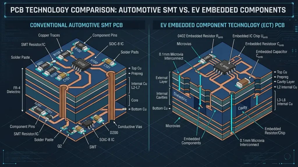
3D Structural Comparison: Conventional SMT vs. EV Embedded Component PCB
A conventional SMT board places components on external surfaces. An EV embedded PCB moves selected components into internal structures, trading manufacturing simplicity for integration density.
| Parameter | EV Embedded Component PCB | Conventional SMT PCB |
| Component location | Internal and/or external | Mainly external |
| Surface utilization | Lower component occupation | Higher component occupation |
| Integration density | Very high | Moderate to high |
| Interconnect length | Can be reduced significantly | Often longer |
| Manufacturing complexity | High (cavity + lamination + microvia) | Lower |
| Internal inspection | Requires X-ray, microsection, 3D AOI | Relatively straightforward |
| Repairability | More difficult | Easier |
| DFM dependency | Critical | High |
| Thermal analysis | Required for embedded active/power devices | Usually simpler |
| Initial engineering effort | Higher | Lower |
The procurement implication is clear: you are not buying a commodity PCB. You are procuring a manufacturing strategy that must survive cavity formation, component placement, high-pressure lamination, laser drilling, plating, thermal cycling, and final assembly without dimensional or electrical degradation.
Which EV Components Are Suitable for PCB Embedding?
Embedded passives (resistors, capacitors, inductors) are the most practical starting point. Active components and bare dies require substantially more thermal, mechanical, and reliability validation.
Embedded Resistors
Embedded resistor layers remove discrete resistors from crowded surface areas. This is critical when the top side is already dominated by connectors, processors, sensors, and power-management ICs.
Embedded Capacitors
Embedded capacitance improves local power integrity by reducing the physical distance between decoupling capacitance and the active circuit. However, the electrical benefit must be verified from the complete power delivery network (PDN)—not assumed from component relocation alone.
Embedded Inductors
Consider embedded inductors for filtering and power-management structures where magnetic performance, thermal behavior, and available PCB area align with the application requirements.
Embedded Active Components and Dies
Active-device embedding is considerably more demanding. The engineering review must address:
- Device power dissipation and junction temperature
- Die/component thickness and CTE mismatch
- Interconnection method (wire bond, flip-chip, copper pillar)
- Mechanical protection during lamination
- Lamination temperature exposure
- Moisture sensitivity and microvia reliability
- Post-embedding inspection accessibility
IPC-7092 specifically addresses passive and active embedded component implementation, covering design, process, inspection, and reliability considerations.
How Is an EV Embedded Component PCB Manufactured?
Manufacturing requires a coordinated process chain: DFM review → material selection → inner-layer fabrication → cavity formation → component placement → lamination → laser drilling → desmear/plating → microvia/copper filling → outer-layer circuit formation → surface finish → AOI/X-ray → electrical test → final inspection.
1. DFM and Stack-Up Engineering
Before production, engineers must review:
- Component body dimensions and Z-height
- Cavity dimensions, tolerance, and positional registration
- Dielectric thickness and copper weights
- Via structure, impedance targets, and clearance budgets
- Lamination sequence and thermal path design
2. Cavity Formation
The cavity must accommodate the actual component while maintaining sufficient mechanical and electrical clearance. Cavity walls must be clean and dimensionally stable to prevent resin bleeding or component shift.
3. Component Placement
Placement accuracy is critical. Once laminated, the component position becomes the reference for all subsequent interconnection structures. Automated placement with vision alignment is standard for high-reliability EV applications.
4. Lamination
Lamination must simultaneously control:
- Temperature profile and pressure ramp
- Vacuum level and resin flow
- Component positional stability
- Board warpage and void formation
High-vacuum lamination is essential. Voids around embedded components are a primary failure mode.
5. Laser Drilling and Microvia Formation
Laser drilling creates compact vertical connections to embedded components. For EV embedded designs, UV/CO₂ laser systems (e.g., Mitsubishi platforms) provide the precision required for microvias landing on embedded pads.
6. Fine-Line and mSAP Processing
When conventional subtractive etching cannot maintain required geometry, modified semi-additive process (mSAP) enables 8/8 μm-class trace/space fabrication for advanced substrate-like applications.
What Cavity Parameters Should Engineers Specify?
Cavity dimensions should be specified as controlled manufacturing characteristics with realistic tolerances derived from DFM and supplier process-capability analysis—not arbitrary CAD defaults.
| Cavity Parameter | Recommended RFQ Definition |
| Length | Nominal + tolerance (e.g., ±50 μm for standard, ±25 μm for precision) |
| Width | Nominal + tolerance |
| Depth | Nominal + tolerance (must account for component Z-height + adhesive) |
| Component body | Manufacturer part number and datasheet |
| Component Z-height | Maximum and nominal values |
| Component clearance | Minimum edge clearance (typically ≥100 μm) |
| Cavity-to-pad registration | Required tolerance (e.g., ±75 μm) |
| Cavity-to-microvia registration | Required tolerance |
| Adhesive/resin | Material specification and thickness |
| Lamination condition | Approved process window |
Critical rule: Do not impose an arbitrary ±10 μm cavity tolerance simply because a CAD drawing shows a small number. Whether ±10 μm is realistic depends on board thickness, material stack-up, copper distribution, cavity method, measurement methodology, and production volume. Establish tolerance after joint DFM review.
How Do HDI and Microvias Improve Embedded PCB Density?
HDI microvias create compact vertical interconnections between embedded components and surrounding circuitry, eliminating the routing area consumed by conventional through-hole structures.
Embedded EV designs commonly use:
| Microvia Type | Application |
| Blind microvias | Layer-to-layer connections in build-up sections |
| Staggered microvias | Reduced thermal-mechanical stress on stacked interfaces |
| Stacked microvias | Maximum density for any-layer HDI |
| Copper-filled microvias | Improved thermal conductivity and planar surface for via-in-pad |
| Via-in-pad | Direct component mounting over microvias |
For engineering documentation, always specify the finished microvia diameter, not merely the laser spot diameter. Additional critical parameters include capture-pad diameter, target-land size, dielectric thickness, via aspect ratio (recommended ≤0.8:1 for high reliability), copper thickness, and fill requirement.
IPC-6012F explicitly covers rigid multilayer boards with blind/buried vias and microvias, including active/passive embedded circuitry.
Which PCB Materials Should Be Considered?
Material selection must balance thermal stability, dimensional stability, dielectric performance, copper adhesion, moisture resistance, and manufacturability through repeated thermal exposure.
| Material Characteristic | Why It Matters | Typical EV Target |
| Tg (Glass Transition) | Mechanical stability at elevated temperature | ≥170°C (high-Tg FR-4); ≥200°C (advanced systems) |
| Td (Decomposition) | Thermal decomposition resistance | ≥340°C |
| Z-axis CTE (α2) | Through-thickness dimensional stress during thermal cycling | ≤250 ppm/°C |
| Dk @ 1 GHz | Impedance and propagation characteristics | 3.0–4.5 (application-dependent) |
| Df @ 1 GHz | Dielectric loss for high-frequency signals | ≤0.003 (low-loss); ≤0.0015 (ultra-low-loss) |
| Water absorption | Moisture/reliability behavior | ≤0.15% |
| Peel strength | Copper-to-dielectric adhesion | ≥0.8 N/mm |
| T288 | Thermal resistance indicator | >60 minutes (high reliability: >120 min) |
Current example: Panasonic MEGTRON 8 publishes Tg of 220°C, Td of 370°C, T288 of >120 minutes, Z-axis CTE α2 of 270 ppm/°C, and Dk at 14 GHz of approximately 3.08–3.13 depending on grade. These figures are material-specific published data—not universal requirements for every EV PCB.
How Does Thermal Management Change with Embedded Components?
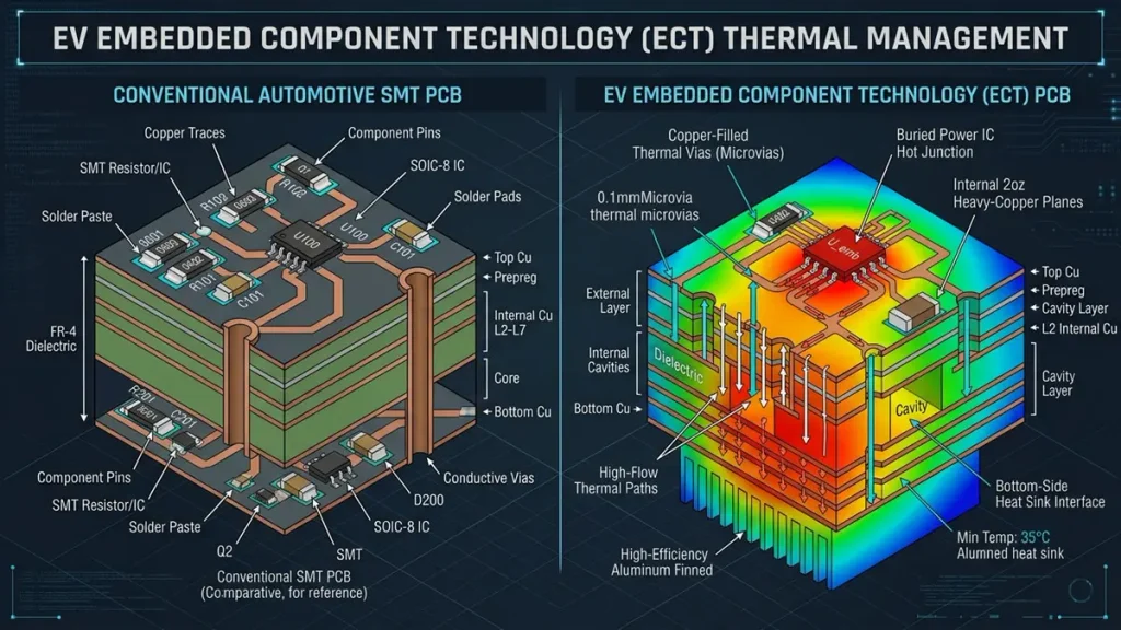
Thermal Simulation: EV Embedded Component PCB Heat Dissipation Path
Embedding a heat-generating component shortens electrical paths but can complicate heat extraction. The thermal path must be designed before the component is buried.
For low-power embedded passives, thermal impact is minimal. For active or power devices, engineers must map the complete thermal chain:
Component → copper land → internal copper plane → thermal vias → PCB heat-spreading structure → chassis/cooling interface
A first-order temperature estimate:
ΔT = P × θ
Where:
- P = dissipated power (W)
- θ = effective thermal resistance (°C/W)
- ΔT = estimated temperature rise
Worked example: A SiC gate driver dissipates 4 W inside an 8-layer board with 2 oz internal copper planes and thermal vias to a bottom-side heat spreader. If the effective thermal resistance from junction to ambient is 8 °C/W:
ΔT ≈ 4 W × 8 °C/W = 32°C
If the ambient enclosure temperature is 85°C, the estimated junction temperature is 117°C—acceptable for many automotive-grade devices, but marginal for extended reliability targets. Real EV modules require thermal simulation (ANSYS Icepak, SimScale) and physical validation because anisotropic spreading, interface resistances, and enclosure cooling dominate the result.
Common mistake: Specifying heavy copper and assuming the thermal problem is solved. Copper thickness aids lateral spreading, but dielectric and interface thermal resistances often remain the actual bottleneck.
What Are the Biggest Manufacturing Pain Points?
The most difficult problems are process interactions: component movement, resin voids, registration accumulation, microvia reliability, and hidden-defect detection.
Pain Point 1: Component Movement During Lamination
Once dielectric is laminated, the buried component is no longer visible. If the component shifts, subsequent microvia or pad registration fails. Solution: high-precision placement with temporary tacking, followed by controlled-pressure lamination.
Pain Point 2: Resin Voids Around the Component
Voids result from insufficient vacuum, poor resin flow, incorrect prepreg selection, or trapped air. Solution: high-vacuum lamination, optimized prepreg resin content, and void-free filling processes.
Pain Point 3: Registration Accumulation
The manufacturing chain contains multiple coordinate transformations:
Inner layer → cavity → component → lamination → laser drilling → outer routing
Even when each process is within individual tolerance, cumulative error can consume design clearance. Solution: design registration as a chain, not isolated steps.
Pain Point 4: Microvia Reliability
Stacked microvias introduce additional interfaces. Critical controls: target land flatness, copper interface quality, plating thickness uniformity, fill completeness, and thermal-mechanical stress management.
Pain Point 5: Hidden Defects
AOI alone cannot reveal every internal defect. A robust inspection strategy combines:
AOI + 3D inspection + AXI/X-ray + microsection analysis + electrical test + process traceability
How Should Reliability Be Tested?
Reliability testing must reproduce the actual electrical, thermal, mechanical, and environmental stresses at the vehicle installation location.
| Test Category | Example Tests | Applicable Standard |
| Thermal cycling | -40°C to +150°C, 1000+ cycles | IPC-6012F Class 3 / AEC-Q100 |
| Mechanical loads | Vibration, mechanical shock, board bend | ISO 16750-3 |
| Climatic loads | Temperature/humidity cycling, salt mist | ISO 16750-4 |
| Electrical loads | Overvoltage, reverse polarity, load dump | ISO 16750-2 |
| Chemical loads | Fluid exposure (coolant, oil, fuel) | ISO 16750-5 |
There is no universal EV reliability profile. Test conditions depend on:
- Vehicle installation location (cabin vs. powertrain vs. underhood)
- Operating temperature range
- Voltage class and vibration exposure
- Humidity and chemical environment
- Expected service life and OEM-specific requirements
The customer specification—not a generic “automotive grade” claim—must control the final validation plan.
Which Automotive Standards Apply?
IPC-6012F provides the base rigid-PCB qualification framework. The applicable automotive addendum and customer-specific requirements must be explicitly invoked for EV programs.
Your procurement specification should clearly state:
- Applicable IPC revision (e.g., IPC-6012F)
- Applicable automotive addendum
- Product performance class (Class 2 or Class 3)
- Microvia requirements (structure, fill, aspect ratio)
- Cavity requirements (tolerance, registration)
- Internal plated-layer requirements
- Electrical test requirements (flying probe vs. fixture)
- Reliability requirements (customer-defined profile)
- Customer/OEM-specific requirements (IATF CSR)
A generic “automotive compliant” statement is insufficient for supplier qualification.
What Should Be Included in an EV Embedded PCB RFQ?
A professional RFQ must define construction, embedded component data, manufacturing tolerances, electrical requirements, reliability profile, inspection requirements, and production volume.
RFQ Checklist
| RFQ Item | Required Information |
| PCB dimensions | L × W × finished thickness |
| Layer count | Total layers and HDI build-up sequence |
| Stack-up | Core/prepreg/dielectric thicknesses by layer |
| Copper weights | oz or μm, specified by layer |
| Embedded component | Manufacturer + part number + datasheet |
| Component Z-height | Nominal and maximum |
| Cavity geometry | L × W × depth + tolerance |
| Clearance requirements | Component-to-cavity, cavity-to-pad, pad-to-via |
| Microvias | Finished diameter + structure (staggered/stacked) + fill type |
| Trace/space | Minimum production requirement (e.g., 8/8 μm mSAP) |
| Impedance | Single-ended/differential targets + tolerance |
| Materials | Grade and approved alternatives |
| Surface finish | ENIG, ENEPIG, OSP, etc. |
| Inspection | AOI, AXI/X-ray, microsection requirements |
| Electrical test | Flying probe or fixture test |
| Reliability | Customer-defined test profile or OEM specification |
| Prototype quantity | Number of boards for validation |
| Annual volume | Production forecast |
| Application | BMS, OBC, DC-DC, inverter, ADAS, etc. |
Pro tip: For complex embedded structures, component part numbers and mechanical dimensions are more important than nominal PCB dimensions alone for accurate DFM review.
How Can Buyers Compare EV Embedded PCB Suppliers?
Compare qualified manufacturing capability, engineering evidence, yield data, reliability records, and total cost of ownership—not bare-board unit price alone.
| Qualification Factor | Weight | Evidence to Request |
| Technical feasibility | 25% | DFM review records, stack-up proposals |
| Process/equipment capability | 20% | Laser drilling (UV/CO₂), LDI, mSAP, plating line specs |
| Quality and traceability | 15% | ISO/IATF certificates, inspection protocols, material certs |
| Prototype-to-volume transfer | 15% | Yield data, process control documentation, NPI case studies |
| Reliability evidence | 10% | Microsection photos, thermal cycling results, microvia reliability data |
| Yield transparency | 10% | First-pass yield by product category, scrap/rework rates |
| Commercial factors | 5% | Unit price, tooling, NRE, logistics |
The most revealing procurement question is not: “Can you manufacture an embedded PCB?”
It is: “What measured yield and reliability do you achieve on structures comparable to ours?”
2026 Trends in EV Embedded PCB Manufacturing
The major 2026 trend is the convergence of embedded circuitry, advanced HDI, fine-line/mSAP processing, laser micromachining, high-reliability materials, automated internal inspection, and data-driven manufacturing.
Modern embedded PCB development increasingly combines:
- Embedded passive and active components
- Any-layer HDI with stacked microvias
- mSAP/SAP-style fine-line processing
- Low-loss, high-Tg material systems
- Picosecond/femtosecond laser processing
- Automated X-ray inspection and 3D AOI
- Digital traceability and advanced electrical testing
IPC-6012F reflects this complexity through expanded requirements for cavities, copper wrap plating, intermediate target lands, internal plated layers, and microvia reliability.
However: “Latest technology” should never be a purchasing objective by itself. The correct question is: Does the technology improve the required electrical, thermal, mechanical, reliability, or density target at an acceptable manufacturing yield?
Conclusion: When to Use Embedded Component PCBs in EVs
Consider embedded component PCB technology when board-area constraints, integration density, interconnect length, or packaging requirements justify the additional manufacturing and qualification effort.
The technology is especially relevant when conventional SMT architecture creates:
- Insufficient PCB surface area
- Excessive surface-component density
- Difficult HDI routing congestion
- Long local electrical paths degrading signal/power integrity
- Severe packaging or mechanical envelope constraints
- Complex BMS or control-module layouts requiring higher functional density
The engineering decision must be based on the complete system, not one PCB parameter.
For procurement, the critical qualification chain is:
Application Requirement → DFM → Supplier Qualification → Prototype → Reliability Validation → Cost/Yield Review → Volume Production
That is the difference between buying an embedded PCB concept and buying a repeatable EV manufacturing process.
About Shenzhen Hongda Circuit Technology
Shenzhen Hongda Circuit Technology Co., Ltd. supports advanced embedded-PCB projects with documented capabilities including:
- LDI fine-line imaging
- UV/CO₂ laser drilling (Mitsubishi platforms)
- Picosecond/femtosecond laser micromachining
- mSAP fine-line PCB fabrication (8/8 μm class)
- HDI microvia manufacturing (blind, stacked, copper-filled)
- Automated plating lines
- AOI + 3D inspection + X-ray validation
- High-density multilayer PCB manufacturing (prototype to volume)
- Turnkey assembly: raw substrate → component embedding → sequential lamination → outer SMT
Prototype lead time: 10–15 working days (including DFM and component alignment) Volume production: 4–6 weeks Prototype quantities: 1–5 pieces supported
📧 Email: pcb@pcbkr.com 🌐 Website: www.pcbkr.com
5 FAQs for EV Embedded PCB Buyers
What is an EV embedded component PCB, and why do electric vehicles need it?
An EV embedded component PCB integrates electronic components inside the PCB layers rather than only on the surface. Electric vehicles need this technology to achieve higher functional density, shorter interconnects, and improved power integrity in space-constrained modules like BMS, OBC, and DC-DC converters—where conventional SMT boards run out of routing area.
What files and information are needed to request a quote for an EV embedded PCB?
You need Gerber or ODB++ files, a complete BOM with embedded component part numbers and datasheets, stack-up specifications, cavity geometry with tolerances, copper weights by layer, microvia requirements, impedance targets, quantities (prototype + forecast), and your reliability/testing requirements. For embedded structures, component Z-heights and mechanical dimensions are essential—nominal PCB dimensions alone are insufficient for DFM.
How do I evaluate and compare EV embedded PCB manufacturers?
Evaluate suppliers on technical feasibility (25%), process capability (20%), quality/traceability (15%), prototype-to-volume transfer (15%), reliability evidence (10%), yield transparency (10%), and commercial factors (5%). Request DFM records, microsection photos, X-ray inspection examples, material certificates, reliability reports, and actual production yield data. The critical question is not “Can you make it?” but “What yield and reliability do you achieve on comparable structures?”
What is the typical lead time for EV embedded PCB prototypes and mass production?
Prototype lead time is typically 10–15 working days, including DFM review and component sourcing alignment. Mass production requires 4–6 weeks. Actual lead time depends on material availability, component sourcing, cavity complexity, HDI sequence, and testing requirements—always confirm per project.
How can I reduce the total cost of ownership for EV embedded PCBs?
Start with DFM optimization rather than price negotiation. The highest-impact cost reductions come from: standardizing cavity dimensions, reducing unnecessary sequential-lamination stages, rationalizing microvia structures, selecting materials based on quantified requirements (not over-specifying), avoiding unnecessarily tight tolerances, designing for automated inspection, improving first-pass yield, and planning a smooth prototype-to-volume process transfer. Remember: Total Cost of Ownership = Unit Price + Tooling + NRE + Scrap/Rework + Testing + Logistics + Inventory Cost.
About Author
David Chen https://www.linkedin.com/in/pcbcoming
David Chen boasts an extensive professional background in PCBA manufacturing, PCBA testing, and PCBA optimization, with specialized expertise in high-precision PCBA fault analysis and rigorous PCBA reliability testing. The author has worked with high-layer-count server PCB fabrication, ultra-low-loss backplane stackups, and thermo-mechanical reliability optimization for AI infrastructure projects involving 112G and 224G PAM4 architectures. Skilled in complex circuit design and cutting-edge advanced PCB manufacturing processes, he delivers solutions that elevate product durability and performance across industrial applications. His technical articles focusing on PCBA manufacturing workflows and testing methodologies are widely cited by industry peers, research institutions, and technical platforms, solidifying his reputation as a recognized technical authority in the global circuit board manufacturing sector.