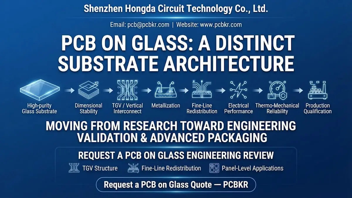
PCB on Glass: What Is a Glass Substrate PCB?
What Is PCB on Glass?
PCB on glass is an electronic interconnect structure built on a continuous glass substrate rather than using glass fibers embedded in epoxy resin. The glass acts as the structural substrate, while conductive layers, redistribution structures, and potentially Through-Glass Vias (TGVs) create electrical interconnections.
The distinction is important:
PCB on glass ≠ glass-fiber PCB.
A conventional FR-4 board uses woven glass fiber as reinforcement inside an epoxy resin matrix. A glass-substrate PCB instead uses a continuous glass material as the substrate itself.
This difference changes the engineering problem.
With glass-fiber PCB technology, engineers primarily work with:
- Glass cloth
- Epoxy resin
- Copper foil
- Lamination
- Drilled vias
- Plated through-holes
- HDI structures
With a glass substrate PCB, the engineering architecture can instead involve:
- Continuous glass core
- TGV formation
- Glass surface treatment
- Metallization
- Copper redistribution
- Build-up dielectric
- Fine-pitch interconnects
- Package-level integration
Recent research continues to identify glass substrates as a potential platform for high-performance packaging because of their dimensional stability, flatness and electrical characteristics.
For procurement teams, the first question should therefore be:
Are you buying a glass-fiber PCB, or are you specifying a true glass-substrate architecture?
That distinction should appear in the RFQ before material and process discussions begin.
How Is a Glass Substrate PCB Different From a Glass-Fiber PCB?
A glass-fiber PCB contains glass fibers within a resin laminate, whereas a glass substrate PCB uses a continuous glass sheet as the structural base.
| Engineering Characteristic | Glass-Fiber PCB | Glass-Substrate PCB |
|---|---|---|
| Structural material | Woven glass + resin | Continuous glass |
| Resin matrix | Fundamental part of laminate | Usually used in build-up structures |
| Glass function | Mechanical reinforcement | Structural substrate |
| Conventional PCB process | Yes | Not necessarily |
| PTH technology | Common | Architecture-dependent |
| Microvias | Common in HDI | Possible in build-up layers |
| TGV | Not applicable to conventional glass cloth | Core interconnect technology |
| Dimensional stability | Laminate-dependent | Major potential advantage |
| Main processing challenge | Lamination, drilling and registration | Glass processing, TGV and metallization |
| Typical technology maturity | Established PCB manufacturing | Advanced/emerging substrate technology |
This distinction is not merely terminology.
A buyer who specifies “glass PCB” without describing the architecture can receive quotations based on completely different manufacturing assumptions.
For example, a supplier may interpret glass PCB as:
FR-4 → glass fiber → epoxy → copper
while another may interpret it as:
glass core → TGV → copper redistribution
Those are different manufacturing ecosystems.
What Is a Glass Substrate PCB Made Of?
A glass substrate PCB generally starts with a continuous glass core and adds conductive and dielectric structures around or across that core. Unlike FR-4, the glass itself is not simply reinforcement inside an epoxy laminate.
A simplified architecture can be represented as:
Glass Core
↓
Glass Via / TGV Formation
↓
Surface Preparation
↓
Conductive Metallization
↓
Copper Interconnect
↓
Build-Up Dielectric
↓
Fine-Line Redistribution
↓
External Interconnect
The exact construction depends on whether the glass is being used as:
- A package substrate
- An interposer
- A panel-level substrate
- An RF substrate
- An optical/electrical integration platform
- A high-density electronic substrate
Glass itself is electrically insulating, so electrical interconnection through the substrate requires a suitable via and metallization architecture.
That is where Through-Glass Via (TGV) technology becomes important.
Why Are Through-Glass Vias Important for PCB on Glass?
TGVs provide vertical electrical pathways through a glass substrate, allowing circuits on opposite surfaces to communicate without relying on conventional drilled through-holes in an organic laminate.
A simplified TGV structure is:
Top circuit
↓
Metal-filled or metallized TGV
↓
Glass substrate
↓
Bottom circuit
TGVs are conceptually comparable to vertical interconnect technologies used in other advanced packaging architectures, but the substrate and manufacturing challenges are different.
Current technical work focuses heavily on:
- Via formation
- Via diameter
- Aspect ratio
- TGV taper
- Glass cracking
- Sidewall quality
- Metallization adhesion
- Copper filling
- Thermal stress
- Via density
- Redistribution-layer reliability
Recent research specifically identifies TGV formation and metallization as critical technical areas for glass-substrate adoption.
The important procurement point is that TGV capability cannot be inferred from ordinary PCB drilling capability.
A manufacturer that can drill FR-4 mechanically or laser-drill HDI microvias does not automatically have a qualified TGV manufacturing process.
How Does PCB on Glass Handle Dimensional Stability?
One of the principal reasons engineers investigate glass substrate PCB technology is its potential for excellent dimensional stability and flatness compared with organic substrate architectures.
As electronic packages become larger and interconnect pitches become smaller, dimensional movement becomes increasingly important.
Consider a structure that must maintain:
- Fine interconnect alignment
- Large-area flatness
- Tight overlay
- Stable via positioning
- Multi-layer redistribution
Small dimensional changes can accumulate across a large substrate.
This becomes especially relevant in advanced packaging.
Recent technical literature highlights the potential of glass to provide dimensional stability and a CTE that can be tailored or selected to better match adjacent materials.
However, procurement should avoid treating “glass has low expansion” as a complete reliability specification.
The complete system still contains:
Glass + copper + dielectric + metallization + package materials
Each interface can experience different thermal expansion.
Therefore, the relevant engineering question is:
How does the complete glass-substrate stack behave through the intended thermal cycle?
rather than simply asking for the CTE of the glass.
What Are the Electrical Advantages of a Glass Electronics Substrate?
A glass electronics substrate can offer a useful combination of electrical insulation, surface flatness, dimensional stability and potentially favorable high-frequency characteristics, making it attractive for advanced interconnect and packaging applications.
Electrical performance depends on the complete architecture, including:
- Glass composition
- Dielectric layers
- Copper geometry
- Conductor surface condition
- Via structure
- Signal reference planes
- Routing geometry
- Frequency
- Package configuration
Glass is therefore not automatically a “low-loss PCB material.”
The correct engineering approach is to evaluate the complete transmission path.
For RF and high-speed structures, engineers should characterize:
- Dielectric behavior at the operating frequency
- Insertion loss
- Return loss
- Characteristic impedance
- Via discontinuity
- Copper loss
- Interface effects
- Crosstalk
A 2025 IEEE conference paper demonstrated RF passive devices integrated on a borosilicate glass substrate using TGV technology, showing the broader potential of glass-based substrates for RF and mmWave integration.
Why Is Glass Substrate PCB Technology Relevant to AI and Advanced Packaging?
Glass substrate PCB technology is attracting attention because AI and high-performance computing packages require larger, flatter and increasingly dense interconnect structures.
The pressure comes from several directions:
Higher I/O density
↓
Larger package dimensions
↓
Tighter interconnect pitch
↓
Greater alignment sensitivity
↓
Higher signal-integrity requirements
Glass is being investigated as one potential response to these scaling challenges.
The current technology discussion increasingly connects glass substrates with:
- AI accelerators
- HPC
- Chiplets
- Advanced semiconductor packaging
- Panel-level packaging
- Optical interconnects
- Co-packaged optics
- RF/mmWave integration
Industry activity is also moving from laboratory research toward process validation and pilot-scale development. For example, recent 2026 reporting describes TGV panel-level capacity development for optical communications and advanced packaging applications.
This does not mean conventional PCB factories are automatically ready for glass-core mass production.
It means procurement teams should begin distinguishing between conventional PCB capability and advanced glass-substrate capability.
What Are the Main Manufacturing Challenges of PCB on Glass?
The major manufacturing challenges are glass handling, precise via formation, crack control, TGV metallization, surface adhesion, dimensional alignment and reliable integration of glass with conductive and dielectric layers.
Glass cracking
Glass is rigid but brittle.
Localized mechanical or thermal stress can create:
- Edge chipping
- Microcracks
- Crack propagation
- Handling damage
- TGV-related fracture
Thermo-mechanical reliability remains one of the major barriers to wider glass-substrate adoption.
TGV formation
Creating a hole through glass is not equivalent to drilling a conventional PCB.
The process must control:
- Hole geometry
- Taper
- Position
- Surface condition
- Microcracks
- Debris
- Heat-affected regions
Research and industry development are exploring laser-based and chemically assisted glass-via formation approaches.
Metallization
After forming the TGV, the next challenge is establishing a reliable conductive path.
Potential issues include:
- Poor adhesion
- Incomplete metallization
- Voids
- Non-uniform copper deposition
- Thermal stress
- Via resistance variation
Recent TGV research increasingly focuses on the transition from via formation to metallization and filling, because a physically formed glass via is not useful unless it can become a reliable electrical interconnect.
Glass-to-metal stress
Copper and glass do not behave identically during temperature changes.
That creates a thermo-mechanical interface problem.
The design therefore has to consider:
Glass properties → via geometry → copper structure → thermal cycling → stress concentration
rather than evaluating each component independently.
Which Manufacturing Technologies Matter for PCB on Glass?
The relevant technologies depend on the exact glass-substrate architecture, but precision laser processing, controlled metallization, fine-line patterning, build-up processing and high-resolution inspection are central to advanced glass-based interconnects.
Precision laser processing
Ultrafast laser processes are being investigated for TGV formation and other glass-processing applications.
The engineering objective is not simply a smaller hole.
A production-quality process must control:
Diameter + taper + position + wall condition + crack formation + repeatability
Fine-line patterning
After TGV formation, the substrate may require fine redistribution structures.
This creates requirements for:
- High-resolution imaging
- Fine copper patterning
- Overlay control
- Surface preparation
- Plating uniformity
Advanced metallization
TGV reliability depends heavily on the interface between glass and conductor.
Process development may involve:
- Surface activation
- Seed-layer formation
- Copper deposition
- Electroplating
- Via filling
- Stress control
High-resolution inspection
Because some defects are internal, visual inspection alone may not be sufficient.
Depending on the project, engineering validation may involve:
- Optical inspection
- X-ray inspection
- Cross-section analysis
- Electrical continuity
- Resistance measurement
- Thermal cycling
- Reliability evaluation
The inspection plan should follow the actual TGV and substrate failure modes.
Can Standard PCB Equipment Be Used for PCB on Glass?
Some PCB manufacturing technologies can support portions of a glass-substrate production flow, but standard FR-4 equipment should not be assumed to provide complete glass-core/TGV capability.
This is an important supplier-selection issue.
For example, a PCB manufacturer may have:
- LDI
- Laser drilling
- mSAP
- Vacuum lamination
- AOI
- X-ray
- Precision plating
These technologies can be highly relevant to advanced PCB manufacturing.
However, TGV processing is a separate capability question.
The buyer should ask:
- What type of glass can the supplier process?
- What TGV formation method is qualified?
- How are glass microcracks controlled?
- How is the TGV metallized?
- How is copper adhesion verified?
- What via geometry has been production-validated?
- What reliability testing has been completed?
- Is the capability prototype-only or production-qualified?
This distinction protects the buyer from a common procurement mistake:
Equipment list ≠ qualified process capability.
How Should Engineers Specify a Glass Substrate PCB?
A glass-substrate PCB specification should define the substrate architecture, glass material, dimensions, TGV structure, conductive layers, dielectric build-up, electrical requirements and reliability targets.
A useful RFQ should identify:
Glass substrate
- Glass type
- Glass thickness
- Panel dimensions
- Surface requirements
- CTE requirement
- Flatness requirement
- Optical characteristics where relevant
TGV structure
- Via diameter
- Via pitch
- Via depth
- Aspect ratio
- Taper requirement
- Via density
- Metallization method
- Fill requirement
Circuit structure
- Line/space
- Copper thickness
- Layer count
- Redistribution layers
- Microvia requirements
- Pad geometry
Electrical requirements
- Characteristic impedance
- Frequency range
- Insertion loss
- Return loss
- DC resistance
- Isolation requirements
Reliability requirements
- Thermal cycling
- Thermal shock
- Mechanical handling
- Glass cracking criteria
- TGV electrical continuity
- Metallization adhesion
The more advanced the glass architecture, the more important it becomes to define measurable acceptance criteria rather than simply writing “glass PCB.”
How Should Buyers Evaluate a PCB on Glass Supplier?
Buyers should evaluate a glass-substrate supplier by demonstrated process capability, engineering validation, inspection methodology and reliability evidence—not by conventional PCB capability alone.
A practical supplier qualification sequence is:
Architecture
↓
Glass Material
↓
TGV Capability
↓
Metallization
↓
Fine-Line Processing
↓
Inspection
↓
Reliability
↓
Pilot Production
The supplier should be able to explain where each critical parameter is controlled and measured.
For example:
| Buyer Question | Evidence to Request |
|---|---|
| Can you process this glass? | Material/process qualification |
| Can you form the specified TGV? | Cross-section/sample data |
| Can you metallize the TGV reliably? | Via resistance/section evidence |
| Can you maintain alignment? | Dimensional/overlay data |
| Can you create the required fine lines? | Microsection/capability data |
| Can you detect internal defects? | X-ray/inspection methodology |
| Can the structure survive thermal cycling? | Reliability data |
| Can you scale production? | Pilot/yield/process-control evidence |
For advanced glass substrates, this evidence-based approach is much more useful than comparing suppliers solely by quoted unit price.
What Is the Current Manufacturing Trend for Glass Substrate PCB?
The current direction is toward larger-area glass panels, finer TGV structures, improved metallization, higher-density redistribution and integration with advanced semiconductor and optical packaging.
The technology is moving through several important development stages:
Glass material engineering
→
Precision glass processing
→
TGV formation
→
TGV metallization
→
Fine-line redistribution
→
Package integration
→
Panel-level manufacturing
A recent 2026 technical review specifically highlights the evolution of TGV technology toward larger-scale panel-level packaging.
At the same time, current industry reporting indicates growing interest in TGV substrates for optical communications, with AI/HPC remaining a longer-term target.
This means the near-term opportunity is not simply “replace FR-4 with glass.”
Instead, glass is becoming part of a broader advanced substrate and packaging ecosystem.
How Does Shenzhen Hongda Circuit Technology Approach PCB on Glass Projects?
Shenzhen Hongda Circuit Technology Co., Ltd. approaches glass-substrate projects from the perspective of process feasibility, interconnect requirements and manufacturing validation rather than treating every “glass PCB” request as conventional FR-4 production.
Our PCB manufacturing engineering workflow can involve technologies such as:
- LDI
- Laser drilling
- HDI processing
- mSAP
- Controlled lamination
- Precision copper plating
- AOI
- X-ray inspection
- Microsection analysis
- Electrical testing
- Impedance verification
These technologies are particularly relevant when a glass-based project incorporates fine-line circuitry, HDI structures or complex build-up layers.
However, an important engineering distinction should remain explicit:
Glass-fiber PCB capability does not automatically equal glass-core/TGV capability.
For a true PCB on glass substrate project, the engineering team should first confirm:
- Glass type
- Substrate thickness
- TGV requirement
- Via dimensions
- Metallization method
- Build-up structure
- Fine-line requirement
- Electrical targets
- Reliability requirements
- Production volume
Only after those requirements are reviewed should manufacturing capability and quotation be finalized.
This approach allows the supplier-selection process to focus on qualified capability rather than marketing terminology.
Shenzhen Hongda Circuit Technology Co., Ltd. — PCBKR
What Should a PCB on Glass RFQ Include?
A PCB on glass RFQ should clearly identify that the project uses a glass substrate rather than glass-fiber reinforcement and should define the TGV, circuit, electrical and reliability requirements.
PCB on Glass RFQ Checklist
- Glass-substrate architecture
- Glass material/type
- Glass thickness
- Panel dimensions
- Flatness requirement
- CTE requirement
- TGV required/not required
- TGV diameter
- TGV pitch
- TGV aspect ratio
- Via taper requirement
- Metallization requirement
- Copper thickness
- Fine-line requirement
- Build-up layer structure
- Microvia requirement
- Impedance requirement
- Operating frequency
- Thermal cycling requirement
- Inspection requirement
- Prototype quantity
- Production quantity
- Target delivery date
A clear RFQ prevents the supplier from assuming that “PCB on glass” means a conventional glass-fiber laminate.
PCB on Glass Procurement FAQ
Is PCB on glass the same as a glass-fiber PCB?
No. PCB on glass normally refers to a structure using a continuous glass substrate, while a glass-fiber PCB uses glass fibers embedded in a resin system such as FR-4.
What is a glass substrate PCB used for?
Glass substrate PCBs are being investigated for advanced packaging, AI/HPC, chiplets, RF/mmWave systems, optical interconnects and other high-density applications where dimensional stability and integration density are important.
Does a glass substrate PCB require TGV?
Not every glass-based electronic substrate requires TGV, but TGV is a major interconnect technology when electrical connections must pass vertically through the glass core.
The TGV requirement should therefore be defined at the architecture stage.
Can a normal PCB manufacturer produce PCB on glass substrate?
Not necessarily. A manufacturer experienced with FR-4 or glass-fiber PCB fabrication may not have qualified glass processing, TGV formation or TGV metallization capabilities.
Buyers should request process-specific evidence before approving the supplier.
How should I request a quotation for PCB on glass?
Start by identifying the architecture as glass substrate PCB / PCB on glass substrate, then provide the glass specification, substrate dimensions, TGV structure, circuit geometry, copper requirements, build-up structure, electrical requirements, reliability targets and production volume.
For advanced structures, an engineering review should take place before a production quotation is treated as technically committed.
Final Engineering Perspective
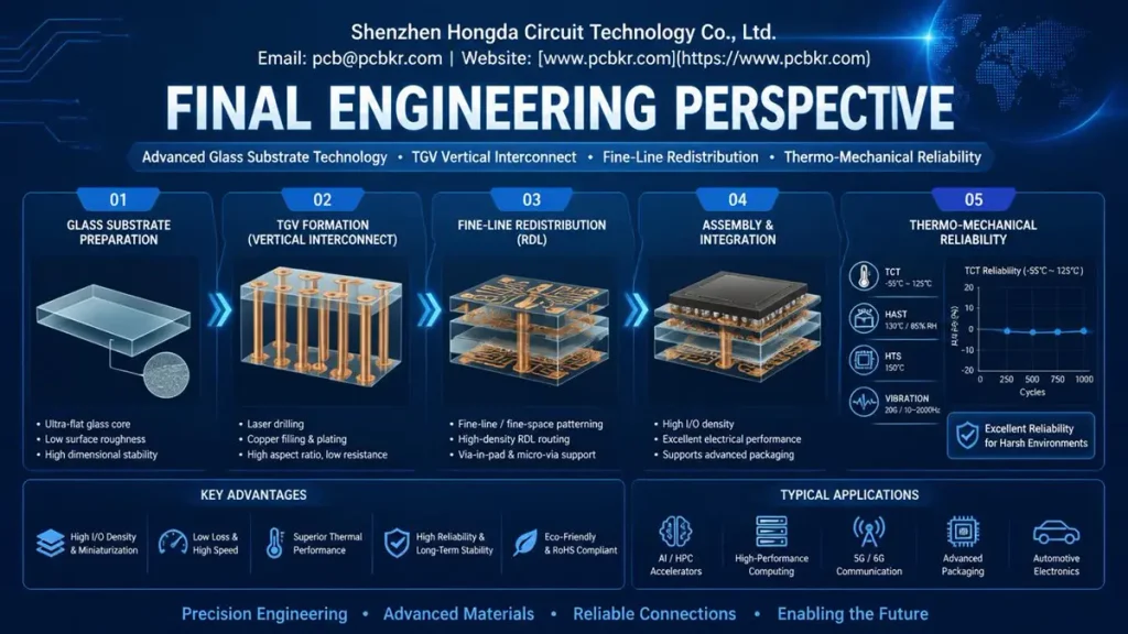
PCB on Glass Final Engineering Perspective Infographic
PCB on glass should be treated as a distinct substrate architecture—not as another name for glass-fiber PCB.
The engineering chain is:
Glass Substrate
→
Dimensional Stability
→
TGV / Vertical Interconnect
→
Metallization
→
Fine-Line Redistribution
→
Electrical Performance
→
Thermo-Mechanical Reliability
→
Production Qualification
That distinction is becoming increasingly important as glass substrates move from research toward engineering validation and advanced packaging applications. Current research continues to focus on TGV reliability, glass cracking, metallization and stress management, while industry development is expanding toward panel-level applications and optical/AI infrastructure.
For procurement teams, the most important question is therefore not:
“Can you manufacture a glass PCB?”
It is:
“Can you manufacture this specific glass-substrate architecture, with its required TGV, metallization, dimensional, electrical and reliability targets, and provide evidence of process qualification?”
That is the question that separates a conventional PCB quotation from a technically meaningful PCB on glass manufacturing assessment.
Request a PCB on Glass Engineering Review
Request a PCB on Glass Engineering Review and Quote
If your project requires a glass substrate PCB, PCB on glass substrate, TGV structure, fine-line redistribution or another advanced glass-based interconnect architecture, Shenzhen Hongda Circuit Technology Co., Ltd. can review the technical requirements before quotation.
Request a PCB on Glass Quote — Email: PCB@pcbkr.com
About Author
David Chen https://www.linkedin.com/in/pcbcoming
David Chen boasts an extensive professional background in PCBA manufacturing, PCBA testing, and PCBA optimization, with specialized expertise in high-precision PCBA fault analysis and rigorous PCBA reliability testing. The author has worked with high-layer-count server PCB fabrication, ultra-low-loss backplane stackups, and thermo-mechanical reliability optimization for AI infrastructure projects involving 112G and 224G PAM4 architectures. Skilled in complex circuit design and cutting-edge advanced PCB manufacturing processes, he delivers solutions that elevate product durability and performance across industrial applications. His technical articles focusing on PCBA manufacturing workflows and testing methodologies are widely cited by industry peers, research institutions, and technical platforms, solidifying his reputation as a recognized technical authority in the global circuit board manufacturing sector.