Prototype PCB Assembly Services: Fast-Turn & Low-Volume Solutions
Every hardware product begins as an unproven idea sitting on a schematic. The gap
between that schematic and a working board is where most product timelines quietly fall
apart — not because the design is wrong, but because the first build takes too long to arrive,
or arrives with a defect nobody caught until it was too late to fix cheaply.
At Shenzhen Hongda Circuit Technology Co., Ltd., prototype PCB assembly sits at the
center of the New Product Introduction (NPI) process we support for engineering teams
around the world. During this stage, two risks dominate every conversation we have with
clients: a turnaround that slips past a launch window, and a DFM (Design for
Manufacturability) issue that surfaces only after boards have already been populated. Both
are avoidable when a build is planned correctly from the first Gerber file review onward,
and both are the reason this page exists — to explain exactly how our prototype PCBA line
is structured to protect your schedule and your design.
What Is Prototype PCB Assembly?
Prototype PCB assembly refers to the low-volume production of populated circuit boards —
typically somewhere between 1 and 25 units — built specifically to validate that a design
functions as intended before it moves toward mass production. Unlike a production run, a
prototype build is not judged primarily on cost-per-unit; it is judged on whether the board
proves out the circuit, exposes layout issues, and gives an engineering team confidence to
move forward.
The distinction between prototype PCB assembly and mass production PCBA runs deeper
than volume alone:
1. Equipment setup: production lines are configured and re-tooled for a single,
repeatable job; a prototype line has to reconfigure stencils, feeders, and reflow profiles
multiple times a day to accommodate different boards.
2. Process flexibility: last-minute BOM substitutions, rework, and hand-placement of
unusual components are routine in prototyping and would be disruptive in a mass
production environment.
3. Testing depth: functional and in-circuit testing on prototypes is often more manual
and diagnostic in nature, aimed at root-causing failures rather than simply passing or
failing a board.
Key Benefits of Low-Volume & Quick-Turn PCBA
Design Validation. A populated prototype is the only way to confirm that a circuit behaves
the way a simulation predicted. Timing issues, thermal hot spots, and signal integrity
problems on high-speed nets rarely show up on paper — they show up on a bench, under
real load, on a real board.
Cost Efficiency. Every design change made after tooling for mass production is committed
costs exponentially more than the same change made during the prototype phase.
Catching a footprint mismatch or a routing error on a batch of five boards is a rounding
error; catching it after 5,000 units have shipped is a recall.
Speed to Market. In competitive hardware categories, the team that iterates fastest wins
the design cycle. A quick-turn PCB assembly partner capable of 24–48 hour builds
compresses months of back-and-forth into weeks, which is often the difference between
hitting a funding milestone or a customer commitment and missing it.
Prototype PCBA Capabilities at Shenzhen Hongda Circuit Technology
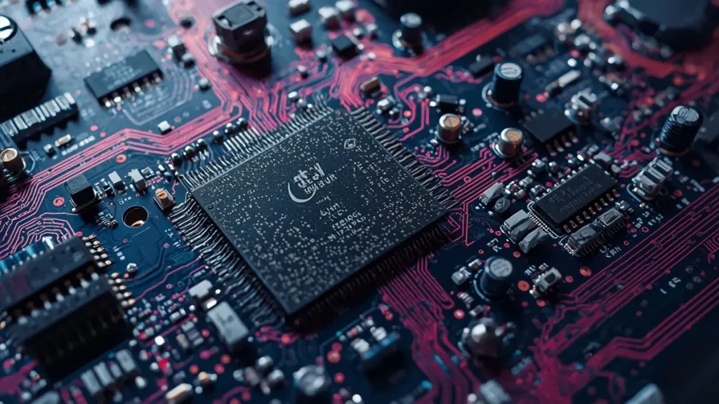
Prototype PCB Assembly Capabilities – High Density Hardware
Our prototype line is built to handle the full range of assembly technologies an R&D team is
likely to need on a single board:
1. SMT (Surface Mount Technology) for standard and fine-pitch components
2. THT (Through-Hole Technology) for connectors and higher-stress mechanical
components
3. Mixed Technology boards combining SMT and THT on the same assembly, which is
the norm rather than the exception for most real-world designs
On the component side, we regularly place devices that push the limits of standard
assembly equipment: BGA packages down to 0.4mm pitch, 01005 and 0201 passives, and
boards built on ultra-high-density HDI substrates that demand tight placement accuracy
and precise stencil registration. As line width and spacing on advanced HDI boards
continue moving toward the finer geometries now common in 2026 — driven by modified
semi-additive (mSAP) processes and sub-50-micron laser microvias — placement accuracy
and paste-print consistency at the prototype stage matter more than ever, because there is
far less margin to absorb a misaligned pad or a bridged joint.
While prototyping focuses on speed, our core PCB Assembly lines are fully equipped to
transition your design seamlessly into mid-to-high volume production, so the board that
validates on our prototype floor can move into scaled manufacturing without a second
qualification cycle.
Standard Process Flow for Prototype PCB Assembly
Step 1: DFM Analysis on Gerber and BOM Files
The moment we receive a Gerber package and BOM, our engineering team runs a DFM
(Design for Manufacturability) check before a single component is ordered. This step
catches footprint mismatches, missing paste layers, silkscreen conflicts, and impedance
sensitive routing issues while they are still a five-minute email exchange rather than a
rebuilt board.
Step 2: Component Sourcing for PCB Prototype Builds
Once the BOM is confirmed, our sourcing team pulls parts through authorized distribution
channels rather than open-market brokers, which is where counterfeit and remarked
components most often enter a supply chain. For obsolete or long-lead-time parts, we work
with the design team on verified substitutes rather than letting a single line item stall the
whole build.
Step 3: Solder Paste Printing and Component Placement
Prototype builds demand more flexibility at this stage than production runs — stencils and
placement programs are frequently adjusted between revisions, and our pick-and-place
equipment is calibrated to handle everything from standard 0603 passives to 0.4mm-pitch
BGAs on the same job.
Step 4: Reflow Soldering, AOI, and X-Ray Inspection
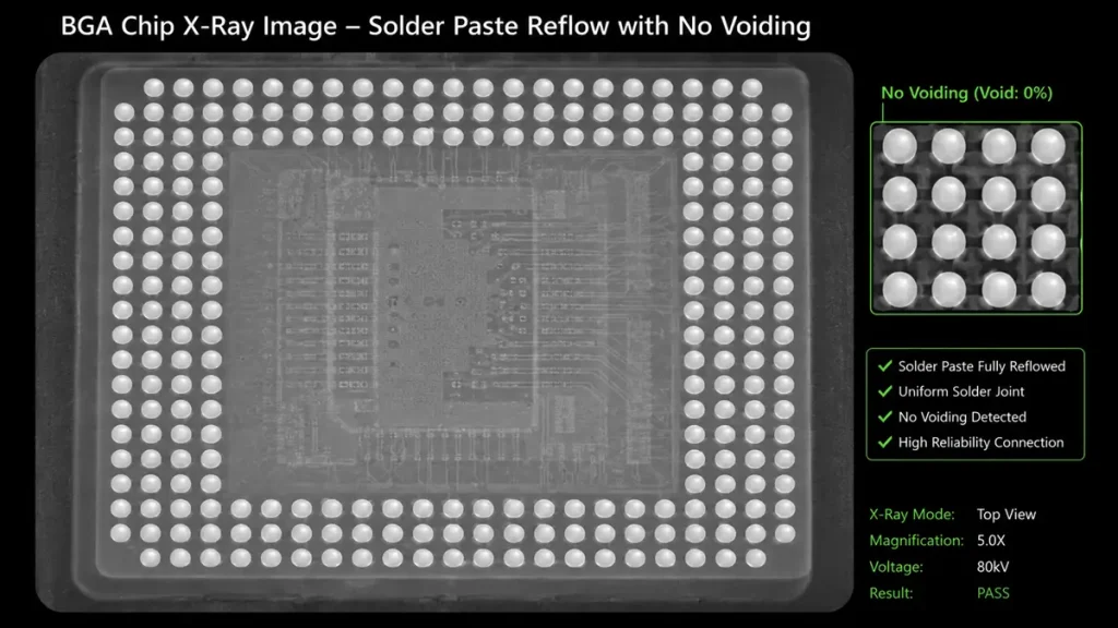
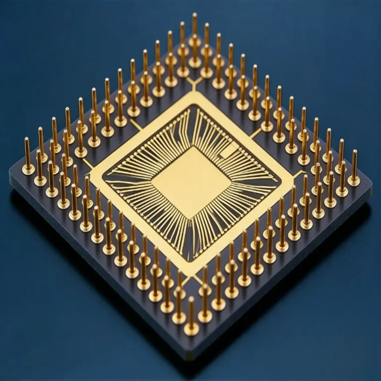
BGA Chip X-Ray Inspection – Solder Joint Quality Pass
After reflow, every board passes through Automated Optical Inspection (AOI), and any
board carrying BGA, QFN, or other hidden-joint packages goes through X-ray inspection to
confirm solder connections that a camera simply cannot see. This is non-negotiable on
prototypes, since a hidden solder void discovered after software bring-up wastes far more
engineering time than the inspection step itself.
Common Challenges in Prototyping and How We Fix Them
1. BOM errors and omissions. Reference designators that don’t match the schematic, missing
values, or duplicate line items are among the most common causes of prototype delay. Our
incoming BOM review flags these discrepancies against the Gerber and schematic before
ordering begins, rather than after boards are already populated.
2. Component package mismatches. A part number that is electrically correct but
mechanically wrong — the wrong footprint variant, the wrong pitch — is one of the most
frequent causes of a failed first-article build. Our DFM step cross-checks footprints against
the actual component package, not just the part number.
3, Thermal management issues. Dense prototype boards, especially those built on HDI
stackups with tightly packed BGAs, often reveal thermal problems that were invisible in
simulation. We flag copper pour and thermal via concerns during DFM review so the issue
is addressed in layout rather than discovered on a hot board during bring-up.
Ready to Kickstart Your Hardware Project?
If you have a Gerber file and a BOM ready to go, our team can turn around a DFM review
and a fast prototype PCBA quote within 24 hours. Upload your files and tell us your target
quantity and timeline, and we’ll come back with a build plan — not just a price. Email:pcb@pcbkr.com
FAQs:
How do I verify a PCB assembly manufacturer before placing an order?
Ask forevidence of process certifications (ISO 9001, IPC-A-610 workmanship standards), request references or case studies from a similar industry, and confirm whether components are sourced through authorized distribution rather than open-market brokers. A manufacturer
willing to share DFM feedback before quoting is usually a stronger long term partner than one that quotes on file receipt alone.
What is the typical lead time for prototype PCB assembly versus mass production?
Prototype builds can often be completed in 24–72 hours once DFM is cleared and components are in stock, while mass production runs are scheduled around line capacity and typically measured in weeks. Lead time also depends heavily on whether all BOM components are on hand or require sourcing.
What information does a PCB assembly supplier need to provide an accurate quote?
At minimum: Gerber files, a complete BOM with manufacturer part numbers, assembly drawings or a placement file, and target quantity. Suppliers that can quote from incomplete files without flagging the gaps are often the ones that generate change orders later.
How is pricing structured for low-volume versus high-volume PCB assembly?
Low volume and prototype pricing carries a higher effective cost per board because of setup and changeover time, while mass production pricing amortizes tooling and setup costs across a much larger unit count. Buyers evaluating total cost should also factor in the cost of a design error caught late, which low-volume runs are specifically designed to prevent.
Can the same supplier handle both prototype builds and volume production?
Many suppliers specialize in one or the other, but working with a single manufacturer for both stages avoids a second DFM and qualification cycle when a design moves from prototype to production. Buyers should confirm a supplier’s production capacity and equipment range extends beyond prototype-scale runs before assuming a smooth transition.
About Author
David Chen https://www.linkedin.com/in/pcbcoming
David Chen boasts an extensive professional background in PCBA manufacturing, PCBA testing, and PCBA optimization, with specialized expertise in high-precision PCBA fault analysis and rigorous PCBA reliability testing. The author has worked with high-layer-count server PCB fabrication, ultra-low-loss backplane stackups, and thermo-mechanical reliability optimization for AI infrastructure projects involving 112G and 224G PAM4 architectures. Skilled in complex circuit design and cutting-edge advanced PCB manufacturing processes, he delivers solutions that elevate product durability and performance across industrial applications. His technical articles focusing on PCBA manufacturing workflows and testing methodologies are widely cited by industry peers, research institutions, and technical platforms, solidifying his reputation as a recognized technical authority in the global circuit board manufacturing sector.