Machine Vision Camera PCB: Engineering, Manufacturing & Procurement Guide
A machine vision camera PCB is the high-density interconnect platform that connects an image sensor, processor, memory, power-management circuitry and a high-speed data interface within an industrial imaging system. Unlike a basic board camera, an industrial vision PCB must balance HDI routing density, signal integrity, power integrity, thermal management, EMC performance, mechanical stability and long-term manufacturing reliability.
For many compact industrial cameras, an 8-layer HDI architecture can provide a practical balance between routing density, signal integrity and manufacturing cost. However, the correct layer count, laminate, impedance target and via structure should be determined from the sensor, interface standard, channel length, thermal environment and mechanical constraints rather than from a fixed template.
For OEMs and procurement engineers, the critical question is not simply whether a PCB can carry the camera electronics. It is whether the PCB manufacturing process can consistently reproduce the electrical, thermal and mechanical characteristics required by the complete imaging system.
What Exactly Is a Machine Vision Camera PCB—and Why Isn’t a Basic Board Camera Enough?
A machine vision camera PCB is a rigid, and in some applications rigid-flex, circuit board engineered around an industrial image sensor and a high-speed data path.
Typical designs may include:
- CMOS or CCD image sensors
- FPGA or image-processing SoCs
- DDR memory
- PMICs and local LDOs
- GigE, USB3 Vision or CoaXPress interfaces
- Trigger and synchronization circuitry
- High-speed differential pairs
- Thermal-management structures
- EMI shielding and controlled return paths
The distinction between an industrial machine vision PCB and a basic board-camera PCB is important.
A basic board camera may be adequate for applications where:
- Data rates are relatively modest
- Operating temperature is controlled
- Long-term field reliability is not critical
- Mechanical constraints are simple
- High-density routing is unnecessary
Industrial machine vision systems can impose much more demanding requirements.
A camera installed on an AOI machine, robotic inspection system or factory-automation line may operate continuously in an environment containing motors, variable-frequency drives, vibration, elevated temperatures and electrical noise.
The PCB therefore becomes part of the imaging system’s electrical, thermal and mechanical architecture.
A typical industrial camera PCB can be considered as three functional regions:
- Sensor region — image sensor, local decoupling, power regulation and high-speed sensor interfaces.
- Processing region — FPGA or SoC, DDR memory and associated power-distribution networks.
- Interface region — GigE, USB3, CoaXPress or other high-speed communication circuitry.
These regions do not necessarily need physical isolation. The more important consideration is the continuity of signal-return paths, power distribution and electromagnetic containment.
A well-designed return-current structure can make the difference between a camera that passes EMC validation efficiently and one that requires multiple hardware revisions.
Which Stack-Up, Laminate and Impedance Targets Should You Specify?
For many compact industrial vision cameras, an 8-layer HDI structure can provide a useful balance between routing density, signal integrity, thermal management and manufacturing complexity.
Higher layer counts or advanced any-layer HDI structures may become appropriate when the design includes:
- High I/O-count image sensors
- Multiple high-speed interfaces
- FPGA or SoC processing
- DDR4 or faster memory
- PoE
- Multi-camera synchronization
- Tight mechanical constraints
- Higher aggregate data throughput
The actual stack-up should be developed from the interface requirements and validated against the selected materials and fabrication process.
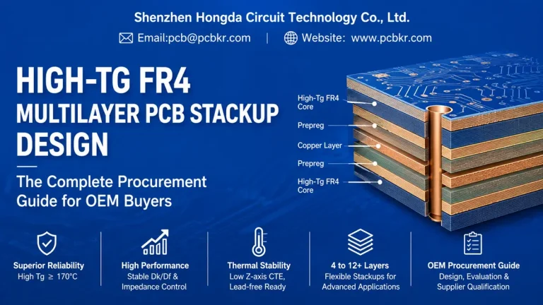
Example Engineering Stack-Up
| Parameter | Example Engineering Target | Why It Matters |
|---|---|---|
| Layers | 8-layer HDI | Provides additional routing density for compact camera electronics |
| HDI structure | 1+6+1 or application-specific build-up | Supports dense BGA escape and high-speed routing |
| Laminate | Low-loss FR-4 or high-speed laminate such as Megtron-class materials, selected according to the channel budget | Controls dielectric loss and signal propagation characteristics |
| Microvias | Approximately 75–100 μm laser-drilled microvias, subject to design rules | Enables high-density BGA escape and HDI interconnection |
| Differential impedance | Example target: 100 Ω ±8% where required by the system design | Supports controlled high-speed differential routing |
| Single-ended impedance | Example target: 50 Ω ±10% where required | Used for clocks, RF/control and other single-ended signals |
| Board thickness | Approximately 0.8–1.2 mm for many compact camera designs | Balances mechanical rigidity, routing and thermal requirements |
| Warpage | Project-specific internal target, typically tighter for sensor regions | Protects BGA coplanarity and optical-mechanical alignment |
| Surface finish | ENIG or another finish selected according to component and assembly requirements | Provides a flat surface suitable for fine-pitch assembly |
These values should be treated as engineering examples rather than universal machine vision PCB standards.
The final impedance target should always be derived from the applicable interface specification, semiconductor vendor recommendations, connector characteristics and complete system channel design.
Why Copper Roughness Matters for High-Speed Camera PCBs
One parameter that is frequently overlooked during PCB procurement is copper roughness.
At multi-gigabit data rates, conductor surface roughness can increase conductor loss because the high-frequency current becomes concentrated near the conductor surface. This is one of the reasons High-Speed PCB material and fabrication selection must be evaluated together with the complete channel-loss budget.
This becomes increasingly important for:
- CoaXPress
- USB3 Vision
- High-speed FPGA interfaces
- MIPI-based sensor links
- Other multi-gigabit differential channels
For high-speed camera designs, reverse-treated or very-low-profile copper can be considered when the channel loss budget requires it.
The correct copper foil should be selected based on:
- Data rate
- Channel length
- Trace geometry
- Laminate loss
- Copper roughness
- Via count
- Connector characteristics
- PHY equalization capability
Rather than applying one copper specification to every camera PCB, the better approach is to establish a complete channel-loss budget.
How Do Global-Shutter Sensors and High-Speed Interfaces Drive Layout Rules?
Global-shutter sensors are widely used when accurate motion capture is important. They can simplify the acquisition of moving objects, but the sensor power-distribution network still requires careful design.
At the interface level, different machine vision standards create different PCB constraints.
GigE Vision
GigE Vision commonly uses Ethernet physical-layer technology and differential routing around the Ethernet PHY and magnetics. The PCB must maintain appropriate differential geometry, reference-plane continuity and EMC control.
USB3 Vision
USB3 Vision uses multi-gigabit USB signaling. PCB routing must follow the requirements of the applicable USB implementation, including controlled impedance, via transitions, return-path continuity and channel-loss management.
Many USB designs use approximately 90 Ω differential impedance as a practical PCB target, but the exact value should follow the applicable specification and system implementation.
CoaXPress
CoaXPress provides much higher-speed camera connectivity than conventional GigE implementations, with CXP-6 supporting 6.25 Gbps and CXP-12 supporting 12.5 Gbps per coaxial link.
At these data rates, PCB insertion loss, via discontinuities, connector transitions, return paths and copper roughness can become important parts of the overall channel budget.
Practical Layout Rules for Machine Vision Camera PCBs
1. Treat length matching as a signal-integrity budget
Length matching should be derived from the actual interface timing and channel requirements.
Avoid applying an unnecessarily aggressive matching rule to every signal.
Excessive serpentine routing can introduce additional discontinuities and coupling, so the target should be based on electrical requirements rather than an arbitrary visual symmetry.
2. Never route high-speed differential pairs across a plane split
A high-speed pair crossing a reference-plane discontinuity can force return current to take a longer path.
This increases loop inductance and can increase:
- EMI
- Crosstalk
- Insertion loss
- Mode conversion
- Signal-integrity risk
For machine vision camera designs, plane-continuity checks should therefore be part of the DFM and high-speed design review.
3. Protect clock and trigger return paths
Camera synchronization signals can be sensitive to ground discontinuities and electrical noise.
Trigger and clock routing should maintain an appropriate reference plane or controlled return structure throughout the signal path.
For multi-camera systems, synchronization requirements should be considered at the PCB level rather than left entirely to firmware.
4. Place sensor power decoupling close to the device
High-frequency decoupling capacitors should be placed as close as practical to the relevant sensor power pins.
The exact capacitor value, placement distance and quantity should follow the image-sensor manufacturer’s power-integrity recommendations.
A typical design may use small MLCCs close to high-frequency supply pins together with larger reservoir capacitors around the sensor power-distribution region.
Sensor-rail ripple should be validated against the specific sensor manufacturer’s requirements rather than applying one universal millivolt limit to every camera.
How Should High-Speed Camera Channel Length Be Determined?
There is no universal PCB channel-length limit for CXP-12, USB3 or other multi-gigabit interfaces.
The achievable channel length depends on:
- Laminate Dk/Df
- Trace width and spacing
- Copper roughness
- Via structure
- Backdrilling
- Connector transitions
- PHY output characteristics
- Receiver equalization
- Temperature
- Total insertion-loss budget
For a demanding high-speed camera design, PCBKR recommends evaluating the complete channel rather than using a generic distance rule.
Where appropriate, engineers can use:
- TDR
- VNA
- Channel simulation
- Eye-diagram analysis
- Insertion-loss measurement
- Return-loss measurement
to validate the final design.
What Do Modern PCB Manufacturing Technologies Change for Vision Camera Boards?
Three manufacturing technologies are particularly relevant to compact, high-density vision camera PCBs:
- mSAP fine-line fabrication
- Any-layer HDI with laser microvias
- Advanced thermal-management structures
For camera PCBs, mSAP can be valuable when conventional subtractive processing cannot provide the required routing density or geometric control.
mSAP reduces some of the geometric limitations associated with conventional subtractive etching and can support very fine outer-layer geometries.
For suitable designs, this can provide additional routing space for:
- Fine-pitch BGA devices
- FPGA packages
- MIPI interfaces
- Dense sensor escape routing
- Power-management components
However, mSAP should not be selected simply because it is a more advanced process.
The correct question is: Does the electrical and mechanical design actually benefit from the additional fabrication capability?
Which Manufacturing Capabilities Actually Affect Machine Vision PCB Quality?
LDI for Fine Registration
Laser direct imaging can reduce some of the artwork-related limitations associated with traditional film-based exposure.
PCBKR’s manufacturing capability includes LDI with approximately ±8 μm registration capability for qualified applications.
For fine-pitch HDI designs, registration control affects:
- Pad alignment
- Microvia landing
- Fine-line geometry
- Layer-to-layer registration
- Impedance consistency
Laser Drilling for HDI Microvias
Laser drilling is essential for compact HDI camera designs where conventional through-hole structures cannot provide sufficient routing density.
PCBKR supports laser-drilled microvias down to approximately 75 μm, depending on the final stack-up, material system and process qualification.
Microvia reliability also depends on:
- Hole geometry
- Aspect ratio
- Desmear quality
- Copper deposition
- Filling process
- Lamination
- Thermal cycling
Therefore, a supplier’s nominal laser diameter alone does not prove microvia reliability.
Plasma Desmear and Microvia Reliability
For high-density HDI structures, effective desmear is important before subsequent metallization.
Plasma treatment can provide a controlled method for preparing microvia structures where conventional mechanical processes may be less effective.
The actual reliability of the finished microvia should be verified through the appropriate qualification and reliability testing program.
TDR Impedance Verification
For machine vision designs requiring impedance-controlled PCB manufacturing, TDR testing provides a practical method of verifying the manufactured impedance against the design target.
A robust quality program should consider:
- Test coupon design
- Coupon location
- Differential impedance
- Single-ended impedance
- Test frequency
- Acceptance limits
- Statistical distribution
- Process capability
For qualified impedance-controlled production, PCBKR can target process capability such as Cpk ≥1.33, depending on the specific process and customer specification.
For production builds, impedance test data can be included as part of the quality documentation when required by the project.
Why Any-Layer HDI Can Be Valuable for Thin Camera PCBs
Any-layer HDI can increase routing flexibility by allowing microvia interconnection across multiple build-up layers.
This is particularly useful when a camera PCB contains:
- Fine-pitch BGA packages
- High-I/O-count sensors
- FPGA devices
- Dense memory interfaces
- Multiple high-speed differential interfaces
However, every additional lamination cycle can also introduce additional process complexity.
Thin camera boards are especially sensitive to:
- Resin shrinkage
- Copper imbalance
- Lamination stress
- Stack-up asymmetry
- Local copper density
For this reason, copper balance and stack-up symmetry should be reviewed before fabrication.
Which Manufacturing Defects Most Often Affect Machine Vision Camera PCB Yield?
The most important risks are not always visible during ordinary bare-board inspection.
Common failure mechanisms can include:
- Microvia reliability problems
- Via-in-pad voiding
- BGA coplanarity problems
- PCB warpage
- Surface-finish defects
- Impedance variation
- Assembly-induced mechanical stress
- Thermal-management limitations
Stacked Microvia Reliability
When multiple microvias are stacked, the structure experiences repeated Z-axis expansion and contraction during assembly and operation.
The risk increases when:
- Aspect ratios are aggressive
- Copper filling is inadequate
- Desmear is poorly controlled
- Lamination is inconsistent
- Thermal cycling requirements are demanding
For demanding Class 3 applications, the reliability program should be defined according to the applicable customer specification and IPC requirements.
Via-in-Pad Under Image-Sensor BGAs
Image sensors and FPGA devices can require dense BGA escape routing.
Via-in-pad can provide a compact solution, but the via must be appropriately filled and planarized when required by the assembly process.
Poorly controlled via filling can create:
- Solder voiding
- Pad-height variation
- Solder-joint defects
- BGA coplanarity problems
For fine-pitch sensor packages, X-ray inspection can be used to evaluate BGA solder joints and voiding.
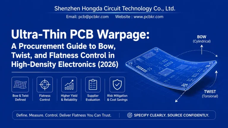
Warpage and Coplanarity
Thin multilayer camera boards can be sensitive to warpage.
The final acceptance requirement should be based on:
- Board thickness
- BGA pitch
- Assembly process
- Mechanical housing
- Sensor package requirements
- Customer drawing
Rather than using one universal warpage percentage, PCBKR recommends defining the limit during DFM review.
ENIG Surface-Finish Quality
ENIG is commonly selected for fine-pitch electronic assemblies because of its flat surface and compatibility with many SMT processes.
However, nickel corrosion, surface contamination and process instability can affect solder-joint reliability.
A qualified surface-finish process should therefore include appropriate bath control, inspection and process monitoring.
How Should a Procurement Engineer Audit a Machine Vision PCB Supplier?
The most useful supplier audit focuses on evidence rather than equipment lists.
A machine vision PCB supplier should be able to explain how it controls:
- Impedance
- Microvia reliability
- Layer registration
- PCB warpage
- Copper balance
- Material traceability
- BGA assembly
- X-ray inspection
- AOI
- Electrical testing
- Functional testing
- DFM review
Ask for Real Impedance Data
Instead of asking: “Can you control 100 Ω?”
ask: “Can you show me a recent impedance test report from a comparable production build?”
A useful report may include:
- TDR measurement
- Target impedance
- Actual impedance
- Test coupon information
- Acceptance limits
- Statistical distribution
- Cpk where available
This provides substantially more evidence than a general capability statement.
Ask How Microvia Reliability Is Qualified
Ask: “How do you qualify stacked and staggered microvias for thermal cycling?”
A strong supplier should be able to explain:
- Laser drilling
- Desmear
- Copper deposition
- Via filling
- Lamination
- Microsection analysis
- Reliability testing
Ask Who Performs the DFM Review
A serious HDI supplier should review more than obvious clearance violations.
The DFM process should consider:
- Stack-up
- Copper balance
- Microvia structure
- Plane continuity
- Impedance geometry
- BGA escape
- Fiducials
- Tooling holes
- Panelization
- Depanelization
- Assembly constraints
A useful DFM report should identify actual manufacturing risks rather than simply state: “No issues found.”
What Does a Machine Vision PCBA Supplier Need to Control?
A camera PCB is only one part of the complete manufacturing process.
For a production machine vision PCBA, procurement should also evaluate:
SMT
- Fine-pitch BGA placement
- Small passive components
- Double-sided assembly
- Moisture-sensitive device control
Inspection
- 3D SPI
- AOI
- X-ray
- Electrical testing
Traceability
- PCB lot
- Component lot
- Assembly lot
- Test results
- Rework history where applicable
Functional Test
Depending on the product, this may include:
- Power-on testing
- Communication testing
- Sensor initialization
- FPGA/SoC programming
- Trigger synchronization
- Image-output verification
- Thermal testing
What Does a Real Industrial Machine Vision Environment Require?
Consider a production inspection system with multiple industrial cameras installed around a high-speed manufacturing line.
The camera electronics may be exposed to:
- Elevated enclosure temperatures
- Variable-frequency drives
- Motors
- Vibration
- Electromagnetic interference
- Continuous operating cycles
A PCB designed only for a 25°C laboratory environment may not provide the same reliability in a production environment.
This is why machine vision PCB design should consider the complete operating environment from the beginning.
Thermal Management
Thermal management can involve:
- Copper planes
- Thermal vias
- Copper coins
- Heat spreaders
- Metal structures
- Thermal interface materials
- Optimized component placement
For high-power FPGA or processor designs, embedded copper structures may provide significantly better thermal conductivity than relying on FR-4 alone.
The appropriate structure depends on:
- Device power
- Junction-temperature limit
- Enclosure design
- Airflow
- Heat-sink strategy
- Mechanical constraints
Why PCB and PCBA Design Must Be Treated as One System
A machine vision PCB can meet its electrical specifications and still fail during assembly or field operation.
For example: A routing change may improve signal integrity but create an unfavorable copper imbalance.
Or: A via-in-pad structure may solve routing density but create assembly voiding if the filling process is not appropriate.
Or:A thinner PCB may satisfy mechanical packaging requirements but become more difficult to control for warpage.
This is why the best manufacturing approach is not simply:“Send Gerbers and manufacture them.”
It is: Design → DFM → Stack-Up Review → Fabrication → Assembly → Inspection → Electrical Test → Functional Validation
What Certifications Should a Machine Vision PCB Supplier Hold?
ISO 9001 is a useful foundation, but certification alone does not prove that a supplier can manufacture a demanding machine vision PCB.
Depending on the application, buyers may evaluate:
- ISO 9001
- IPC-6012 capability
- IATF 16949 for applicable automotive programs
- ISO 13485 for applicable medical programs
- AS9100D for applicable aerospace programs
- UL recognition where required
More importantly, procurement teams should request evidence that the supplier’s actual manufacturing processes support the required quality level.
A certificate on a website is not a substitute for:
- DFM evidence
- Test reports
- Microsections
- TDR data
- X-ray inspection
- Material traceability
- Process-control records
How Do You Verify a Supplier’s Impedance-Control Capability?
Ask for:
- A representative impedance coupon
- TDR measurement data
- Target versus actual impedance
- Test limits
- Stack-up information
- Process capability data where available
For a 100 Ω differential design, the PCB fabrication target should be derived from the customer’s actual stack-up and interface requirements.
PCBKR can support impedance-controlled PCB manufacturing using controlled stack-up design, fine-line fabrication, LDI registration and TDR-based verification for qualified projects.
What Lead Time Should You Expect From Prototype to Production?
Lead time depends heavily on:
- Layer count
- HDI structure
- Material availability
- Microvia complexity
- Surface finish
- Assembly complexity
- Component availability
- Testing requirements
A typical project may require different timelines for:
Prototype PCB fabrication
Approximately 5–7 working days can be achievable for suitable designs and materials.
Pilot PCBA
Approximately 2–3 weeks may be realistic when components, testing and assembly requirements are already defined.
Production
Approximately 3–4 weeks may be achievable for stable production programs once the supply chain and process have been qualified.
These are project-dependent planning ranges, not universal lead-time guarantees.
For machine vision products, image sensors, FPGAs and SoCs can have longer procurement cycles than the PCB itself.
Should You Buy From a Camera Module Maker or a PCB/PCBA Manufacturer?
The answer depends on your product-development model.
A camera module supplier may be preferable when:
- The design is relatively standard
- Customization is limited
- Development resources are limited
- Low-volume purchasing is required
A PCB/PCBA manufacturer may be preferable when:
- You own the camera electronics design
- A custom PCB shape is required
- The sensor and processor architecture is proprietary
- You need customized HDI
- You require transparent BOM and manufacturing costs
- You need prototype-to-production support
- You require dedicated DFM engineering
For OEMs developing specialized machine vision equipment, working directly with a PCB/PCBA manufacturer can provide greater control over the electronic manufacturing process.
What Should You Prepare to Get an Accurate Machine Vision PCB Quote?
For the first RFQ, provide as much engineering information as possible.
PCB Data
- Gerber or ODB++ files
- Stack-up
- Layer count
- Board dimensions
- Material requirements
- Copper thickness
- Surface finish
- Impedance table
- HDI/microvia requirements
PCBA Data
- Complete BOM
- Approved alternates
- Pick-and-place file
- Assembly drawing
- Component orientation
- BGA information
- Testing requirements
Application Information
- Annual volume
- Prototype quantity
- Operating temperature
- Data-interface standard
- Reliability requirements
- Mechanical constraints
- Thermal requirements
- Expected production lifetime
One of the most useful pieces of information is the operating environment.
A supplier selecting materials and manufacturing processes without understanding the thermal, electrical and mechanical environment is working from assumptions rather than engineering requirements.
How Does a Machine Vision Camera PCB Move From Gerber Files to Production?
A reliable production workflow should include:
1. Engineering Review
Review:
- Stack-up
- Layer assignment
- HDI structure
- Impedance
- Materials
- Microvias
- Copper balance
2. DFM Review
Check:
- Trace/space
- Annular ring
- BGA escape
- Microvia geometry
- Panelization
- Tooling
- Fiducials
- Depanelization
3. Fabrication
Manufacture using the qualified process route:
- LDI
- Laser drilling
- HDI build-up
- mSAP where required
- Controlled lamination
- Surface finishing
4. Inspection
Depending on the project:
- AOI
- X-ray
- Microsection
- Dimensional inspection
- Warpage inspection
- Impedance testing
5. PCBA
Perform:
- SMT
- THT where required
- BGA assembly
- Reflow
- Inspection
- Programming
- Functional testing
6. Production Validation
Confirm:
- Electrical performance
- Communication interfaces
- Trigger/synchronization
- Thermal behavior
- Mechanical fit
- Reliability requirements
Frequently Asked Questions About Machine Vision Camera PCBs
What PCB structure is commonly used for industrial machine vision cameras?
There is no single standard stack-up for every camera. Compact designs may use multilayer HDI structures, while higher-I/O or higher-speed products may require additional layers or any-layer HDI.
The correct structure should be determined from the sensor package, processor, memory, interface, mechanical envelope and signal-integrity requirements.
Does a machine vision camera PCB require controlled impedance?
Many industrial camera designs do.
GigE, USB3 Vision, CoaXPress and high-speed sensor interfaces can require controlled-impedance routing.
The exact target should follow the interface and system-level design requirements.
When should mSAP be used for a machine vision PCB?
mSAP becomes particularly useful when routing density, fine-line requirements or BGA escape cannot be efficiently achieved with conventional subtractive fabrication.
It should be selected when the design requires its additional process capability—not simply because it is a newer technology.
Are 75 μm microvias necessary for every camera PCB?
No.
A 75 μm microvia capability provides additional routing flexibility, but the required microvia diameter depends on:
BGA pitch
Layer count
Pad geometry
Stack-up
Routing density
Manufacturing rules
The objective is to use the simplest reliable via structure that satisfies the design.
How can I verify a machine vision PCB supplier’s high-speed manufacturing capability?
Ask for evidence rather than marketing claims.
Useful evidence includes:
Representative stack-ups
Impedance reports
TDR data
Microsection images
HDI capability data
Material traceability
X-ray inspection capability
DFM reports
Relevant quality certifications
What is more important: PCB price or PCBA cost?
For a complete industrial camera, the PCB is only one component of total manufacturing cost.
The total PCBA cost may also include:
Image sensor
FPGA or SoC
Memory
PMIC
Connectors
Magnetics
PCB fabrication
SMT assembly
Testing
Programming
Calibration
For this reason, procurement should evaluate the complete manufacturing cost rather than selecting a supplier based solely on bare-board price.
What Should Global OEMs Look for in a Machine Vision PCB Manufacturer?
The strongest supplier is not necessarily the one with the lowest PCB quotation.
For a demanding industrial camera project, evaluate whether the manufacturer can support the complete manufacturing chain:
HDI fabrication → fine-line processing → controlled impedance → PCBA → inspection → electrical testing → production quality documentation
For advanced camera designs, capabilities such as:
Any-layer HDI
75 μm-class laser microvias
mSAP
Fine-line fabrication
LDI registration
High-speed laminate processing
Controlled impedance
TDR verification
AOI
X-ray
BGA assembly
can become important differentiators.
Request a Machine Vision Camera PCB Quote
If you are developing an industrial camera, AOI camera, robotic vision system or factory-automation imaging product, provide your PCB files, stack-up, impedance requirements, BOM and annual volume for an engineering review.
Shenzhen Hongda Circuit Technology Co., Ltd. supports PCB and PCBA manufacturing for demanding electronic applications, including HDI, fine-line, high-speed and impedance-controlled PCB designs.
For qualified projects, our engineering team can review:
- PCB stack-up
- HDI structure
- Microvia design
- Impedance requirements
- Material selection
- DFM risks
- Assembly requirements
- Testing requirements
The goal is not simply to manufacture the Gerber files.
The goal is to build a production-ready PCB/PCBA that meets the electrical, thermal, mechanical and reliability requirements of the machine vision system.
Request your machine vision PCB / PCBA quotation from Shenzhen Hongda Circuit Technology Co., Ltd. Email: pcb@pcbkr.com
About Author
David Chen LinkedIn Profile
David Chen is a Senior RF/PCB Process Engineer at Shenzhen Hongda Circuit Technology Co., Ltd., with over 12 years of experience in high-frequency PCB fabrication, impedance-controlled stack-up design, and Rogers/PTFE laminate processing. He also boasts an extensive professional background in PCBA manufacturing, PCBA testing, and PCBA optimization, with specialized expertise in high-precision PCBA fault analysis and rigorous PCBA reliability testing. The author has worked with high-layer-count server PCB fabrication, ultra-low-loss backplane stackups, and thermo-mechanical reliability optimization for AI infrastructure projects involving 112G and 224G PAM4 architectures. Skilled in complex circuit design and cutting-edge advanced PCB manufacturing processes, he delivers solutions that elevate product durability and performance across industrial applications. His technical articles focusing on PCBA manufacturing workflows and testing methodologies are widely cited by industry peers and technical platforms, and have gained attention and recognition from industry colleagues.