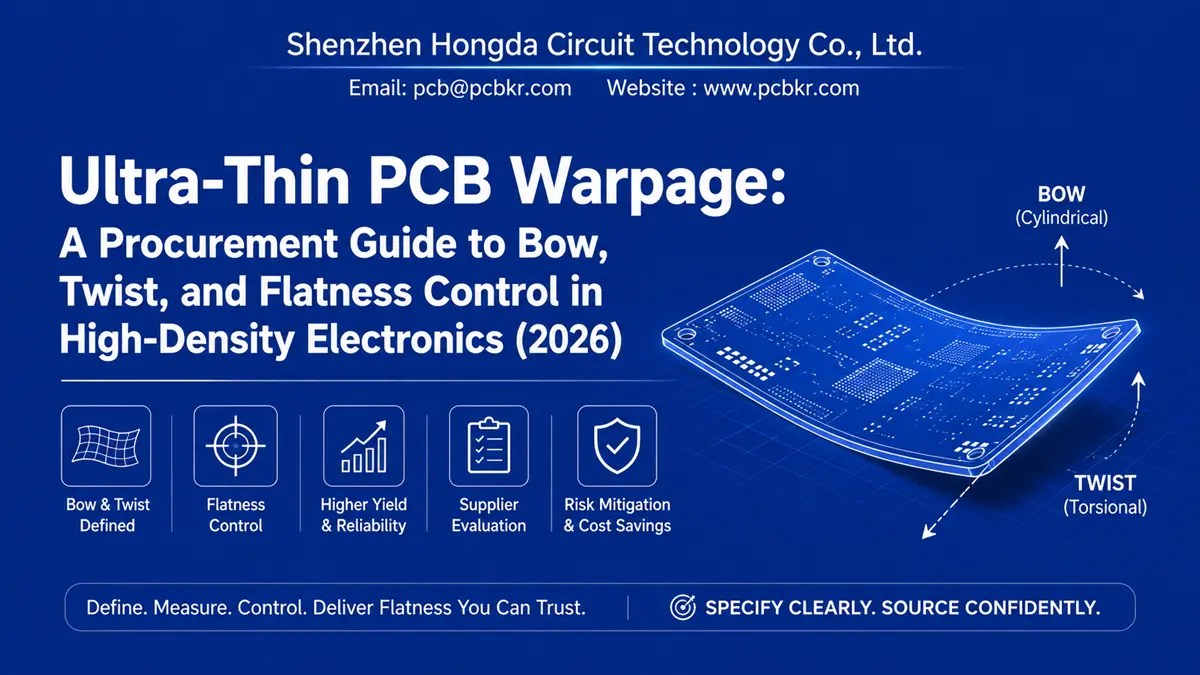
Ultra-Thin PCB Warpage: A Procurement Guide to Bow, Twist, and Flatness Control in High-Density Electronics
Introduction: The Hidden Cost of Thin PCB Warping in Your Supply Chain
If you have ever received a batch of ultra-thin PCBs that passed electrical testing only to fail during SMT placement, you already know the frustration. The pick-and-place machine throws alignment errors. The reflow oven produces head-in-pillow defects on BGA joints. Your assembly partner calls to say the boards will not sit flat in the carrier fixture. The root cause is rarely the solder paste or the component—it is thin PCB warping that was invisible to your incoming inspection team.
For procurement managers sourcing boards below 0.4 mm total thickness, warpage is not a secondary quality metric. It is a primary yield killer. A board measuring 1.2% warp on a 200 mm diagonal exceeds IPC-6012 limits and will trigger rework rates above 15% on fine-pitch assemblies. In high-volume consumer electronics, that single defect can erase your margin. In automotive or medical applications, it creates latent field failures that surface after 500 thermal cycles.
At Shenzhen Hongda Circuit Technology Co., Ltd., we have spent years refining our PCB warpage control systems specifically for ultra-thin substrates. Our facility operates 3D optical warpage scanners on every production lot, finite-element analysis (FEA) simulation during pre-production DFM, and vacuum-assisted lamination presses with closed-loop temperature profiling. This guide explains what ultra-thin PCB warpage is, why it happens, how it destroys assembly yield, and—most importantly—what capabilities you should demand from your supplier to prevent it before the first panel ships.
What Is Ultra-Thin PCB Warpage? Defining Bow, Twist, and Flatness Deviation
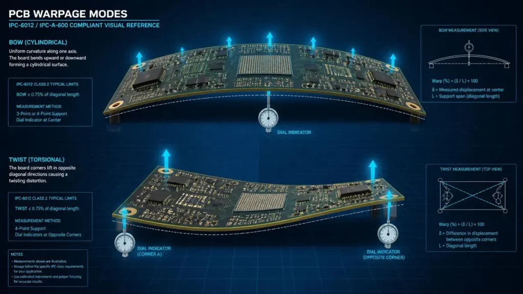
PCB Warpage Modes: IPC-6012 Bow and Twist Measurement Diagram
Ultra-Thin PCB Warpage, Thin PCB Warping, and Thin PCB Warpage — Understanding the Terminology
Before evaluating suppliers, procurement teams need clarity on what they are actually specifying. Ultra-thin PCB warpage refers to any deviation from perfect planarity in a printed circuit board with total thickness ≤ 0.4 mm. The deformation manifests in two distinct forms:
- Bow: A cylindrical curvature where the board arches along one axis. All four corners may touch a flat surface while the center lifts.
- Twist: A diagonal deformation where one corner lifts relative to the other three, creating a torsional warp.
Industry measurement follows IPC-TM-650 Method 2.4.22. The standard procedure places the board on a granite surface plate and measures the maximum deviation height. The warpage percentage is calculated as:
Warp (%) = (Maximum deviation height / Diagonal length) × 100
Procurement Pain Point: Many buyers specify “flatness per IPC” without understanding that IPC-6012 allows 0.75% for SMT boards and 1.5% for through-hole-only boards. For ultra-thin HDI boards with 0.3 mm pitch BGAs, 0.75% is often too loose. At 0.75% warp on a 150 mm board, the center lifts by 1.125 mm—enough to prevent a 0.4 mm pitch BGA from achieving coplanar solder wetting across all balls. High-reliability sectors (automotive, aerospace, medical) typically enforce ≤ 0.5% or even ≤ 0.3% internally.
What to Specify in Your Purchase Order: Define your warpage limit explicitly. Do not rely on generic “IPC compliant” language. State: “Maximum bow and twist: 0.5% per IPC-TM-650 Method 2.4.22, measured at room temperature after moisture bake.” This single sentence eliminates ambiguity and forces your supplier to confirm capability before quoting.
Why Ultra-Thin PCBs Are Disproportionately Prone to Warping
The physics is straightforward: stiffness scales with the cube of thickness. A 1.6 mm standard PCB has 64 times the bending stiffness of a 0.4 mm ultra-thin board (assuming identical material and construction). When that stiffness drops, three forces that standard boards shrug off become dominant:
- Self-weight sag: A 0.2 mm 8-layer board can visibly sag under its own weight when supported only at the edges during handling.
- Processing stress: Every lamination cycle, every drill hit, every plating bath introduces mechanical stress. Thin cores have less material to absorb and distribute that stress.
- Thermal mismatch: Copper and FR-4 have different coefficients of thermal expansion (CTE). In a thick board, the core material provides enough rigidity to resist differential expansion. In an ultra-thin board, the copper layers dominate—and if copper distribution is asymmetric, the board bends toward the copper-heavy side during cooling.
The Amplification Effect: Because ultra-thin boards start with minimal rigidity, even small internal stresses produce visible deformation. A 0.1 mm deviation that would be undetectable in a 1.6 mm board becomes a 0.5% warp in a 0.2 mm board—enough to reject the entire lot.
At Shenzhen Hongda, we address this at the design review stage. When a customer submits a 0.25 mm 10-layer stackup, our DFM engineers run FEA thermal-mechanical simulation before releasing the job. The simulation models the entire lamination-to-reflow thermal cycle, predicting warp magnitude and direction based on copper density, material CTE, and layer symmetry. If the predicted warp exceeds 0.4%, we flag the design and recommend stackup modifications before material is ever cut.
Root Causes of Ultra-Thin PCB Warpage — From Material Science to Reflow Physics
Material and CTE Mismatch — The Foundation of Thermal Stress
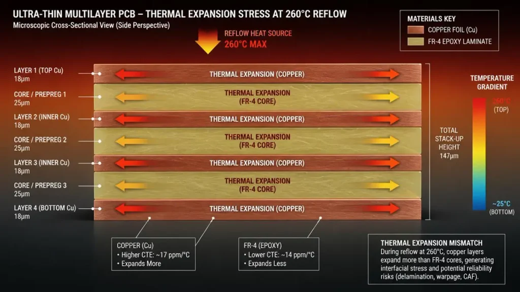
Cross-sectional diagram of ultra-thin PCB showing thermal expansion stress and CTE mismatch between copper layers and FR-4 core at 260°C reflow.
Every material in a PCB expands when heated and contracts when cooled. The problem arises when adjacent materials expand at different rates. Copper has an in-plane CTE of approximately 17 ppm/°C. Standard FR-4 has an in-plane CTE of 14–16 ppm/°C—close enough for thick boards, but problematic for ultra-thin constructions where resin content is lower and glass weave dominates.
More critically, the z-axis CTE (through-thickness expansion) of FR-4 ranges from 45–55 ppm/°C before Tg and can spike above 250 ppm/°C above Tg. During lead-free reflow at 245°C–260°C, the z-axis expansion exerts enormous pressure on copper barrel plating in vias. In ultra-thin boards with high layer counts, this z-axis stress couples with in-plane asymmetry to produce complex warp modes that pure bow/twist models cannot predict.
Material Selection for Warpage Control:
| Material Property | Standard FR-4 | High-Tg FR-4 | Low-CTE Modified Epoxy | Polyimide |
|---|---|---|---|---|
| Tg (°C) | 130–140 | 170–180 | 170–200 | 250+ |
| In-plane CTE (ppm/°C) | 14–16 | 13–15 | 10–12 | 12–16 |
| Z-axis CTE (ppm/°C) | 50–55 | 45–50 | 35–42 | 45–55 |
| Cost Premium | Baseline | +10–20% | +25–40% | +80–120% |
Procurement Decision: For boards undergoing multiple reflow cycles (double-sided assembly, rework, or BGA reballing), specify high-Tg (≥ 170°C) or low-CTE modified epoxy. The 10–20% material cost premium is recovered through improved assembly yield and reduced field failure risk. For extreme environments (aerospace, down-hole instrumentation), polyimide provides the highest dimensional stability but requires specialized fabrication processes that not all suppliers can execute.
At Shenzhen Hongda, we maintain inventory of high-Tg FR-4 (Shengyi S1170, Nan Ya NPG-170) and low-CTE modified epoxy (Panasonic Megtron 6, M7) for ultra-thin applications. Every material lot is verified for CTE consistency using TMA (thermomechanical analysis) before entering production.
Asymmetric Stack-Up — The Design Error That Guarantees Warp
An asymmetric stack-up is the single most common preventable cause of thin PCB warpage. It occurs when the layer structure above the board’s geometric centerline does not mirror the structure below. Common asymmetries include:
- Unequal copper weights: 1 oz copper on Layer 1, 0.5 oz on Layer 2, but no corresponding balance on the bottom half.
- Mismatched dielectric thickness: 100 µm prepreg between L1-L2, but 200 µm between L7-L8 in an 8-layer board.
- Mixed material cores: Using standard FR-4 for outer cores and high-Tg material for inner cores without symmetrical placement.
- Unbalanced via structures: Blind vias on the top side but not the bottom, creating localized resin-rich zones.
Why It Matters: During lamination, the press applies heat and pressure uniformly across the panel. If the top half has more copper (higher modulus, lower CTE) than the bottom half, the top half resists expansion more than the bottom. Upon cooling, the top half contracts more aggressively, pulling the board into a bow toward the copper-heavy side.
The Rule: For any multilayer ultra-thin board, the stack-up must be mirror-symmetric around the center plane. Layer N from the top must match Layer N from the bottom in copper weight, core thickness, prepreg type, and resin content. Even the artwork should be balanced: if the top layer has a large ground pour covering 80% of the area, the bottom layer should have a comparable copper density—not 20% signal traces with bare laminate everywhere.
Shenzhen Hongda’s DFM Protocol: Our engineers run a copper area analysis on every layer during pre-production review. If any layer pair shows > 20% copper density imbalance, we flag it and recommend either copper thieving (adding non-functional copper patterns to sparse areas) or grid fill instead of solid pour. This review is mandatory for all ultra-thin orders and is documented in the DFM report we send back within 24 hours.
Uneven Copper Distribution — Localized Stress Concentrations
Even within a symmetric stack-up, local copper density variation creates warpage. Imagine a board where the left half has dense signal routing (70% copper coverage) and the right half has a large ground plane (95% copper coverage). During reflow, the right half expands less than the left half due to copper’s lower CTE. The result is a twist that lifts one corner.
Common Design Patterns That Cause Local Imbalance:
- Large copper pours on one side with sparse traces on the opposite side.
- Heavy connector footprints with large thermal pads surrounded by low-density signal areas.
- RF shielding cans with solid copper underneath but minimal copper on adjacent layers.
- Power planes with irregular shapes (L-shaped, U-shaped) that concentrate copper in one region.
The Solution — Copper Balancing Techniques:
- Dummy Copper (Thieving): Add non-functional copper polygons to sparse areas. These patterns are electrically isolated (typically connected to ground through a single trace) and serve only to balance copper density. They are removed from the solder mask opening to prevent accidental soldering.
- Grid Fill Instead of Solid Pour: For ground planes in RF or high-speed designs, use a cross-hatch grid (e.g., 0.2 mm trace width, 0.8 mm spacing) instead of solid copper. This reduces copper density from 95% to ~20% while maintaining sufficient shielding and return path continuity.
- Copper Dot Arrays: In areas with < 30% copper coverage, add small copper dots (0.5 mm diameter, 1.0 mm pitch) tied to ground. This is less visually intrusive than large thieving polygons and is preferred for boards with strict aesthetic requirements.
Procurement Tip: Ask your supplier whether their DFM review includes copper density mapping. A supplier that only checks trace width and spacing is missing the warpage risk entirely. At Shenzhen Hongda, our CAM software automatically generates a copper density heat map for every layer, highlighting imbalance zones before the first panel is fabricated.
Lamination Thermal Stress — Where Resin Flow and Cooling Rate Determine Flatness
Lamination is the thermodynamic event that locks internal stress into the board permanently. The process heats the stack to 180–200°C under 300–500 psi pressure, melts the prepreg resin, flows it into voids, and then cures the epoxy. How this heating and cooling is controlled determines whether the board exits the press flat or warped.
Critical Lamination Parameters for Ultra-Thin PCB Warpage Control:
| Parameter | Standard Multilayer | Ultra-Thin HDI (≤ 0.4 mm) | Impact on Warp |
|---|---|---|---|
| Heat ramp rate | 3–5°C/min | 1.5–2.5°C/min | Faster ramps create thermal gradients across thin cores |
| Peak temperature | 180–190°C | 185–195°C | Must fully cure resin without exceeding Tg too early |
| Dwell time at peak | 60–90 min | 90–120 min | Insufficient dwell leaves uncured resin that relaxes later |
| Cooling rate | 3–4°C/min | 1.5–2.0°C/min | Rapid cooling locks in differential contraction stress |
| Pressure profile | Single stage | Multi-stage (ramp + hold + release) | Prevents thin core collapse and resin squeeze-out |
The Cooling Phase Is Critical: Most warpage is created not during heating, but during cooling. When the press opens and the board is exposed to ambient air, the outer copper layers cool faster than the inner core. If the cooling rate is too fast, the copper “sets” while the core is still contracting, creating a permanent bow. Controlled cooling at 1.5–2.0°C/min allows the entire stack to contract uniformly.
Vacuum-Assisted Lamination: For ultra-thin boards, air trapped between layers during pressing creates voids and uneven pressure distribution. Our lamination presses operate under vacuum (≤ 50 mbar) during the entire heat cycle. This eliminates voids, ensures uniform resin flow, and reduces the pressure required—minimizing mechanical distortion of thin cores.
Post-Lamination Flatness Verification: Every panel is measured on a 3D optical scanner immediately after lamination. The scanner projects structured light across the panel surface and reconstructs a height map with ±5 µm resolution. Any panel showing > 0.3% warp at this stage is flagged for process review. The data is logged by batch number and correlated with lamination press parameters (temperature, pressure, cooling rate) for continuous process improvement.
SMT Reflow Thermal Deformation — The Final Test That Exposes Hidden Stress
Even a board that is perfectly flat when it leaves the factory can warp during assembly. Lead-free reflow subjects the board to three thermal insults:
- Preheat zone (150–180°C): Moisture trapped in the substrate vaporizes. If the board was not properly baked, steam pressure creates internal delamination and localized bulging.
- Soak zone (180–200°C): The board reaches thermal equilibrium. Residual stress from lamination begins to relax. If the stack-up was asymmetric, this relaxation manifests as bow or twist.
- Reflow zone (245–260°C): The board exceeds Tg. The resin softens, and the board becomes mechanically compliant. Any internal stress imbalance now causes rapid deformation. Upon cooling, this deformation is locked in permanently.
The Reflow Amplification Effect: A board measuring 0.3% warp after fabrication can increase to 0.8% after a single lead-free reflow cycle. For ultra-thin boards, the effect is more severe because the softened resin provides even less rigidity during the reflow peak.
Procurement Pain Point: Buyers often blame the PCB supplier for reflow warpage when the root cause is actually their own reflow profile. A profile with a 4°C/min ramp rate and 30-second dwell above 250°C will warp almost any ultra-thin board, regardless of how well it was fabricated.
Reflow Profile Recommendations for Ultra-Thin PCBs:
- Ramp rate: ≤ 2°C/min from ambient to 150°C.
- Soak time: 60–90 seconds between 150°C and 180°C to ensure uniform heating.
- Peak temperature: 245°C maximum for standard SAC305 solder. Avoid 260°C unless absolutely necessary.
- Time above liquidus (TAL): 40–60 seconds. Longer TAL increases thermal exposure without improving solder joint quality.
- Cooling rate: 2–3°C/min. Faster cooling creates thermal shock and can induce warp in the opposite direction.
Shenzhen Hongda’s Assembly Support: We provide recommended reflow profiles with every ultra-thin PCB shipment, customized to the board’s thickness, layer count, and material Tg. For customers without in-house reflow optimization capability, we can arrange assembly trials at partner facilities to validate the profile before volume production.
How Thin PCB Warpage Destroys Manufacturing and Assembly Yield
Impact on PCB Fabrication — Warp Breeds More Warp
A warped panel creates a cascade of problems during fabrication:
- Drilling inaccuracy: A bowed panel cannot be held flat on the drill table. Drill hit positions shift by 20–50 µm, causing microvias to miss landing pads. For 0.1 mm diameter microvias, this is fatal.
- Imaging distortion: When a warped panel enters the LDI system, the height variation across the surface causes focus errors. Traces at the board edges may be out of focus, producing inconsistent line width.
- Plating non-uniformity: In electrolytic plating, a warped panel creates variable anode-to-cathode distance. Areas closer to the anode plate faster, creating copper thickness variation that affects impedance control.
- Solder mask misregistration: Solder mask exposure systems assume a flat panel. A 0.5 mm bow causes mask opening misalignment over fine-pitch pads, leading to mask-on-pad defects that prevent solder wetting.
- Routing and scoring defects: V-score blades and routing bits follow a straight path. A warped panel produces uneven scoring depth and irregular board outlines.
The Economics: A panel that warps during lamination is not just one defective board—it is every board on that panel. A standard 18 × 24 inch production panel yields 6–12 boards depending on size. If warp is detected after lamination, the entire panel is scrapped or requires costly re-pressing. At $200–$400 per panel for high-layer-count ultra-thin material, this is a significant write-off.
Impact on SMT Assembly — When Flatness Failure Becomes a Line Stop
For SMT assembly houses, a warped board is a line stop event. The consequences include:
- Pick-and-place rejection: Vision systems detect coplanarity errors and refuse to place components. For 01005 passives or 0.3 mm pitch BGA, even 0.1 mm height variation causes placement failure.
- Solder paste printing defects: A warped board does not seal against the stencil. Paste deposits become uneven, causing insufficient solder on some pads and bridging on others.
- Head-in-pillow (HiP) BGA defects: When a warped board bows during reflow, the BGA balls lose contact with the pad during the critical wetting phase. The solder paste oxidizes, and the ball “pillows” on top of a cold, un-wetted pad. HiP defects are invisible to X-ray and only detectable with destructive cross-sectioning.
- Component tombstoning: Uneven thermal mass caused by board warp creates differential heating across small components. One pad melts before the other, pulling the component vertical like a tombstone.
- Long-term reliability failure: Even if a warped board passes functional test, residual stress creates solder fatigue. After 500–1000 thermal cycles, joints crack and vias fail.
The Procurement Reality: Many buyers discover warpage problems only after they have committed to a 10,000-piece assembly run. By then, the cost of rework, scrap, and delayed shipments far exceeds any savings from choosing a lower-cost PCB supplier. Warp control must be verified at the supplier qualification stage, not after the first article arrives.
At Shenzhen Hongda, we understand that our boards do not exist in isolation—they must survive your assembly process. That is why we perform simulated reflow testing on first-article boards: we run the board through a reflow oven using the customer’s actual profile and remeasure warp before and after. If warp increases beyond 0.2 percentage points, we investigate the stack-up or material selection and recommend changes before volume production.
PCB Warpage Control Methods — Eight Engineering Strategies for Flatness
Optimize Board Thickness and Structural Rigidity
The first question in ultra-thin PCB design is: “How thin is necessary?” Every 0.1 mm reduction in thickness decreases stiffness by approximately 30%. If your enclosure allows 0.5 mm instead of 0.3 mm, the 0.2 mm difference provides dramatically improved warp resistance with minimal weight penalty.
Design Trade-Offs:
- 0.6–0.8 mm: Suitable for most consumer electronics. Standard lamination and handling processes apply. Warp control is straightforward.
- 0.4–0.6 mm: The transition zone where specialized handling and carrier panels become necessary. Symmetric stack-up is mandatory.
- 0.2–0.4 mm: Requires vacuum lamination, carrier panel support during drilling, and often stiffener reinforcement. Every design decision has warp implications.
- < 0.2 mm: Typically rigid-flex or substrate-like PCB (SLP) territory. Requires mSAP or SAP processes and specialized assembly fixtures.
Structural Reinforcement Options:
- Metal stiffeners: Aluminum or stainless steel plates bonded to non-component areas. Common in display driver boards and automotive modules.
- FR-4 stiffeners: Thicker FR-4 strips laminated to the board edge. Lower cost than metal but less effective for thermal management.
- Carrier panels: The board is fabricated within a larger FR-4 frame that provides rigidity during processing. The frame is routed away after assembly, leaving only the thin active area.
At Shenzhen Hongda, we recommend carrier panels for all boards below 0.3 mm. Our standard carrier frame is 1.0 mm thick FR-4 with 5 mm borders, providing sufficient rigidity for automated handling while allowing clean breakaway after assembly.
Enforce Symmetric Stack-Up Design
Symmetric stack-up is non-negotiable for ultra-thin multilayer boards. The rule is simple: for every layer above the center plane, there must be a matching layer below.
Stack-Up Checklist for Procurement Review:
- [ ] Layer 1 copper weight = Layer N copper weight (where N = total layers)
- [ ] Layer 2 copper weight = Layer (N-1) copper weight
- [ ] Core thickness between L1-L2 = Core thickness between L(N-1)-L(N)
- [ ] Prepreg type between L1-L2 = Prepreg type between L(N-1)-L(N)
- [ ] Copper density on Layer 1 ≈ Copper density on Layer N (within 20%)
- [ ] Major copper features on top layers have mirrored counterparts on bottom layers
Common Exception — Asymmetric Designs: Some designs (e.g., single-sided heavy copper for power modules) cannot be symmetric. In these cases, the fabricator must compensate through:
- Asymmetric lamination pressure: Higher pressure on the thin side to compress the thick side proportionally.
- Post-lamination flattening: Thermal-mechanical pressing under constraint after lamination.
- Stiffener addition: Bonding a compensating material to the thin side.
These exceptions add cost and risk. Procurement teams should question whether the asymmetric design is truly necessary or if a symmetric alternative can achieve the same electrical performance.
Balance Copper Density Across All Layers
Copper balancing is both an art and a science. The goal is to achieve < 20% copper density variation between any two layers in a symmetric pair, and < 30% variation between the top and bottom halves of the stack.
Techniques for Copper Balancing:
- Dummy Copper Thieving: Add non-functional copper polygons to sparse areas. Best practice:
- Connect to ground through a 0.2 mm trace.
- Keep thieving patterns ≥ 0.5 mm away from signal traces to prevent capacitive coupling.
- Avoid thieving under high-speed differential pairs where impedance control is critical.
- Remove solder mask opening over thieving to prevent solder adhesion.
- Grid Fill for Planes: Replace solid copper pours with cross-hatch grids:
- 0.2 mm trace / 0.8 mm gap = ~20% copper density (vs. 95% for solid pour).
- 0.3 mm trace / 1.0 mm gap = ~23% copper density.
- Grid orientation should match the direction of current flow for ground planes.
- Copper Dot Arrays: For areas with < 25% coverage:
- 0.5 mm diameter dots on 1.5 mm pitch = ~8.7% added copper density.
- Less visually intrusive than large polygons.
- Preferred for boards with visible copper areas (e.g., RF shields).
Shenzhen Hongda’s Automated Balancing: Our CAM system includes an auto-thieving module that analyzes copper density and suggests thieving patterns. Engineers review the suggestions for electrical impact before implementation. This reduces DFM turnaround from days to hours.
Select Low-CTE, High-Tg Materials for Thermal Stability
Material selection is where procurement teams can make the biggest impact on warpage control without changing the design. The key parameters are:
- Glass transition temperature (Tg): The temperature at which the resin changes from rigid to rubbery. Above Tg, CTE increases dramatically and the board becomes mechanically compliant. For lead-free reflow (peak 245–260°C), Tg should be ≥ 170°C to ensure the board remains rigid during the critical cooling phase.
- Coefficient of thermal expansion (CTE): Lower CTE means less dimensional change per degree of temperature. For ultra-thin boards, in-plane CTE should be < 14 ppm/°C, and z-axis CTE should be < 45 ppm/°C below Tg.
- Modulus of elasticity: Higher modulus means stiffer material. However, very high modulus materials (e.g., ceramic-filled laminates) can be brittle and difficult to machine.
Recommended Materials for Ultra-Thin PCB Warpage Control:
| Material | Supplier | Tg (°C) | In-plane CTE | Z-axis CTE | Best For |
|---|---|---|---|---|---|
| S1170 | Shengyi | 170 | 14 ppm/°C | 48 ppm/°C | General ultra-thin, cost-effective |
| NPG-170 | Nan Ya | 175 | 13 ppm/°C | 45 ppm/°C | High-volume consumer |
| Megtron 6 | Panasonic | 185 | 12 ppm/°C | 38 ppm/°C | High-speed, low-loss, 5G |
| M7 | Domestic | 180 | 11 ppm/°C | 40 ppm/°C | Automotive, high reliability |
| Polyimide | Various | >250 | 12 ppm/°C | 50 ppm/°C | Extreme temperature, flex-rigid |
Procurement Tip: Do not specify material by trade name alone. Specify the required Tg, CTE, and Dk/Df values, and let the supplier propose the specific grade. This ensures you receive the performance you need while allowing the supplier to optimize for availability and cost.
Control Lamination and Cooling Processes with Precision
Lamination is where the board’s internal stress signature is written permanently. For ultra-thin boards, the process window is narrow:
Multi-Stage Pressure Profile:
- Contact stage (50–100 psi): Apply low pressure at 80°C to remove air and begin resin flow. Prevents thin core displacement.
- Flow stage (200–300 psi): Increase pressure at 120°C to drive resin into voids and achieve full wet-out. Hold for 30–45 minutes.
- Cure stage (350–500 psi): Maximum pressure at 180°C to ensure complete cross-linking. Hold for 60–90 minutes depending on prepreg type.
- Cooling stage (controlled release): Reduce pressure gradually as temperature drops below 140°C. Sudden pressure release creates delamination in thin cores.
Cooling Rate Control: Our presses use programmable cooling ramps with segmented water cooling. The target is 1.5–2.0°C/min from peak temperature to 80°C. Faster cooling (> 3°C/min) creates thermal shock and residual stress. Slower cooling (< 1°C/min) extends cycle time unnecessarily and can cause excessive resin flow.
Tooling Consistency: Every lamination press in our facility is calibrated monthly for temperature uniformity (±2°C across the platen) and pressure uniformity (±5% across the panel). Press logs (temperature, pressure, time) are archived for every lot and available for customer audit.
Optimize Reflow Profiles for Ultra-Thin Substrates
Reflow is the final thermal stress that reveals any remaining warp tendency. For ultra-thin boards, the profile must be gentler than for standard boards:
Recommended Reflow Profile for 0.3 mm Ultra-Thin PCB:
- Preheat: 25°C → 150°C at 1.5°C/min (85 seconds)
- Soak: 150°C → 180°C at 1.0°C/min (30 seconds)
- Reflow: 180°C → 245°C at 1.5°C/min (43 seconds)
- Peak: 245°C for 10 seconds
- Cooling: 245°C → 100°C at 2.0°C/min (72 seconds)
- Total cycle time: ~230 seconds
Key Adjustments:
- Reduce ramp rate by 30–40% compared to standard boards.
- Extend soak zone to ensure uniform temperature distribution across the thin substrate.
- Lower peak temperature to 245°C if solder joint reliability allows. Every 5°C reduction above Tg decreases warp by approximately 0.1%.
- Use nitrogen atmosphere to reduce oxidation and allow lower peak temperatures.
Carrier Fixture Support: During reflow, support the board on a flat metal carrier with vacuum hold-down or mechanical clamps. This physically constrains warp during the critical Tg-exceeding phase. The carrier must be thermally matched to the board (typically aluminum) to avoid introducing new thermal gradients.
Implement Mechanical Support Throughout Manufacturing and Assembly
Ultra-thin boards require support at every handling step:
- Material receiving: Store thin core material flat on shelves, not vertically. Vertical storage creates a permanent curl that persists through fabrication.
- Inner-layer processing: Process thin cores on carrier panels (1.0 mm FR-4 frames). The carrier provides rigidity for automated handling, imaging, and etching.
- Drilling: Use vacuum tables with porous surfaces that hold the board flat during drilling. For boards below 0.25 mm, add a backup material (aluminum or phenolic) beneath the board to prevent burr formation and provide additional support.
- Plating: Rack boards horizontally with support rails every 50 mm. Vertical plating racks cause sag in long thin boards.
- Solder mask: Use pinless exposure systems or vacuum frames. Pin registration creates localized stress points that deform thin boards.
- Electrical test: Use soft-tip probes (≤ 30 g contact force) or pogo-pin fixtures with compliant springs. Hard probes dent pads and create local deformation.
- Shipping: Stack boards flat with interleaving paper between layers. Maximum stack height: 25 mm for boards below 0.3 mm. Ship in rigid cardboard boxes with foam inserts, not polybags that allow flexing.
Establish Continuous Warpage Inspection from Lamination to Final Test
Warp measurement should not be a single checkpoint. It should be a continuous data stream:
- Post-lamination: 100% panel scan with 3D optical scanner. Reject threshold: 0.3%.
- Post-drilling: Sample measurement on 1 board per panel. Drill stress can induce localized warp.
- Post-plating: Sample measurement. Plating adds copper weight asymmetrically if bath chemistry is unbalanced.
- Post-solder mask: Sample measurement. Curing shrinkage can introduce warp.
- Post-routing: 100% board measurement. Routing releases internal stress and can cause spring-back deformation.
- Pre-shipment: 100% board measurement with customer-specified criteria.
Statistical Process Control (SPC): We maintain X-bar and R charts for warp data by material lot, press number, and board design. If a process shows trending toward the upper control limit (0.5%), we trigger a corrective action before any board exceeds specification.
Measurement Equipment at Shenzhen Hongda:
- 3D optical scanner: ±5 µm resolution, full-panel scan in 30 seconds.
- Granite surface plate + dial indicator: IPC-TM-650 compliant manual verification.
- FEA simulation software: Pre-production warp prediction based on stack-up, material, and thermal profile.
Ultra-Thin PCB Warpage Factory Control Flow — Design to Delivery
Design Phase — Catching Warp Risk Before Material Is Ordered
Our DFM review for ultra-thin boards includes a warp risk assessment that standard DFM checks ignore:
- Stack-up symmetry verification: Automated comparison of layer pairs for thickness, copper weight, and material match.
- Copper density mapping: Heat map generation showing density variation across each layer and between layer pairs.
- FEA thermal-mechanical simulation: Finite-element modeling of the lamination-to-reflow thermal cycle. Output: predicted warp magnitude, direction, and stress concentration points.
- Material recommendation: Proposal of specific laminate grades based on the design’s thermal budget and reliability requirements.
- DFM report: Delivered within 24 hours, including warp risk rating (Low / Medium / High) and specific recommendations.
Procurement Benefit: You receive a documented warp risk assessment before committing to tooling or material. If the risk is High, you can modify the design or adjust the specification before incurring fabrication costs.
Manufacturing Phase — Process Discipline That Eliminates Variation
During production, our warp control protocol includes:
- Material pre-bake: All thin core material is baked at 120°C for 4 hours before lamination to remove absorbed moisture. Moisture content is verified with a moisture analyzer (< 0.2% target).
- Press parameter lock: Once a recipe is validated for a specific design, press parameters (temperature, pressure, time, cooling rate) are locked. Any deviation requires engineering approval.
- In-process inspection: 3D scanner measurement after lamination, with automatic correlation to press log data.
- Root cause analysis: Any panel exceeding 0.3% warp triggers an 8D investigation. Corrective actions are implemented before the next lot.
Assembly Phase — Supporting Your Contract Manufacturer
We do not consider our job done when the board ships. Our assembly support includes:
- Reflow profile recommendation: Customized profile based on board thickness, material Tg, and component density.
- Carrier fixture design: For boards below 0.3 mm, we can design and fabricate aluminum carrier fixtures that match your assembly line’s conveyor width and clamp spacing.
- Pre-assembly bake protocol: Recommended time and temperature for moisture removal before reflow.
- Warp measurement before/after reflow: We can perform simulated reflow testing on sample boards and provide before/after warp data.
Quality Assurance and Customer Communication
Transparency is critical for procurement teams managing supplier risk:
- Certificate of Conformance: Every shipment includes warp measurement data for the sampled boards, material lot numbers, and lamination press parameters.
- Process audit availability: Qualified customers can audit our lamination process, measurement equipment, and SPC records.
- Design feedback loop: If a design consistently produces warp near the specification limit, we provide data-driven recommendations for stack-up or copper balance optimization.
- Sample validation: For new designs, we recommend a 5-piece prototype run with full warp characterization before committing to volume.
Conclusion — Reducing Ultra-Thin PCB Warpage Risk Through Proactive Control
Ultra-thin PCB warpage is not a random defect that fabricators fix after the fact. It is a predictable outcome of design decisions, material properties, and process parameters that can be modeled, measured, and controlled. The boards that warp in your assembly line are the same boards that were destined to warp from the moment the stack-up was drawn—if the fabricator lacked the simulation tools, process discipline, or measurement capability to catch the risk early.
Thin PCB warping stems from six fundamental factors: reduced structural rigidity at low thickness, CTE mismatch between copper and substrate, asymmetric layer construction, uneven copper distribution, uncontrolled lamination thermal stress, and aggressive reflow profiles. Each factor is addressable. Each factor should be addressed before the first panel enters production.
Effective PCB warpage control for ultra-thin boards requires a systematic approach:
- Reasonable ultra-thin structural design that does not sacrifice rigidity for marginal space savings.
- Symmetric stack-up architecture with mirrored copper weights, core thicknesses, and dielectric layers.
- Balanced copper distribution achieved through dummy copper, grid fill, or dot arrays.
- Low-CTE, high-Tg materials selected for the specific thermal budget of the application.
- Stable lamination and cooling processes with controlled ramp rates, multi-stage pressure profiles, and vacuum assistance.
- Optimized reflow conditions that do not expose the board to unnecessary thermal stress.
- Continuous flatness inspection from lamination through final test, with SPC trending and automatic correlation to process parameters.
At Shenzhen Hongda Circuit Technology Co., Ltd., we have built our ultra-thin PCB manufacturing capability around this exact framework. Our FEA simulation, 3D optical scanning, vacuum lamination, and SPC-controlled processes are not marketing claims—they are standard operating procedure for every ultra-thin order we produce. We invite procurement teams and hardware engineers to submit their designs for a free DFM review with warp risk assessment. The 24 hours you spend reviewing our feedback could save you 24 days of rework and debugging.
Ready to eliminate warpage from your ultra-thin PCB supply chain? Upload your design files to EMAIL:PCB@pcbkr.com and receive a detailed DFM report with warp prediction, material recommendation, and process capability confirmation.
Shenzhen Hongda Circuit Technology Co., Ltd. — Precision Ultra-Thin PCB Manufacturing with Advanced Warpage Control
Frequently Asked Questions — Ultra-Thin PCB Warpage for Procurement Teams
How do I specify warpage requirements in my PCB purchase order to ensure supplier accountability?
Do not rely on vague language like “per IPC standards.” Instead, write: “Maximum bow and twist: 0.5% per IPC-TM-650 Method 2.4.22, measured at 25°C after 4-hour bake at 120°C. Measurement to be performed on 100% of boards using 3D optical scanning or granite surface plate method.” Additionally, require the supplier to provide measurement data with each shipment and specify the corrective action protocol if warp exceeds limit (e.g., 100% sort, root cause analysis, or lot rejection). This level of specificity forces the supplier to confirm capability during quoting and eliminates disputes after delivery.
What is the difference between bow and twist, and which defect type is more dangerous for fine-pitch BGA assembly?
How do I specify warpage requirements in my PCB purchase order to ensure supplier accountability?
Do not rely on vague language like “per IPC standards.” Instead, write: “Maximum bow and twist: 0.5% per IPC-TM-650 Method 2.4.22, measured at 25°C after 4-hour bake at 120°C. Measurement to be performed on 100% of boards using 3D optical scanning or granite surface plate method.” Additionally, require the supplier to provide measurement data with each shipment and specify the corrective action protocol if warp exceeds limit (e.g., 100% sort, root cause analysis, or lot rejection). This level of specificity forces the supplier to confirm capability during quoting and eliminates disputes after delivery.
Can a warped ultra-thin PCB be successfully flattened after fabrication, or should it be scrapped?
Prevention is always better than correction. For mild warpage (0.5–0.8%), thermal-mechanical flattening under constraint at 150°C for 2 hours can reduce warp by 30–50%. However, this process introduces new residual stress and may cause microvia cracking or pad delamination in ultra-thin boards. For warp above 0.8%, flattening is unreliable and the board should be scrapped. More importantly, if a lot shows systematic warpage, the root cause is in the design or process—and flattening individual boards does not fix the systemic problem. At Shenzhen Hongda, we do not ship flattened boards. If a panel exceeds our internal 0.3% post-lamination limit, we reject it and investigate the process before continuing production.
How does panel size and aspect ratio affect warpage risk in ultra-thin PCB designs?
Larger panels and high aspect ratios (length-to-width > 3:1) amplify warp because they provide more leverage for internal stress to create deformation. A 200 × 50 mm board (aspect ratio 4:1) will warp more than a 100 × 100 mm board of identical construction because the long axis has less resistance to bending. For ultra-thin boards, keep aspect ratio below 2.5:1 if possible. If the design requires a long narrow board, consider adding score lines or mouse bites that allow the panel to be broken into smaller sections before reflow, reducing the effective span that can warp. Alternatively, specify carrier panel processing where the thin board remains supported by a rigid frame throughout assembly.
What specific factory capabilities should I audit to verify a supplier’s ultra-thin PCB warpage control competence?
Request evidence in five categories: (1) Measurement equipment — Do they have 3D optical scanning capability, or do they rely on manual dial indicators? Manual methods are too slow for production volume and too subjective for < 0.5% tolerance. (2) Pre-production simulation — Can they provide FEA warp prediction before fabrication? Suppliers without simulation capability are reacting to problems rather than preventing them. (3) Process control data — Ask for SPC charts showing warp Cpk values over the last 6 months. A Cpk < 1.33 indicates the process is not statistically capable of holding tolerance. (4) Lamination press specifications — Vacuum assistance, multi-stage pressure profiling, and closed-loop cooling control are essential for ultra-thin boards. (5) Material verification — Do they measure incoming laminate CTE and Tg, or do they accept supplier certificates without validation? Unverified material is a common source of lot-to-lot warp variation.
About Author
David Chen https://www.linkedin.com/in/pcbcoming
David Chen boasts an extensive professional background in PCBA manufacturing, PCBA testing, and PCBA optimization, with specialized expertise in high-precision PCBA fault analysis and rigorous PCBA reliability testing. The author has worked with high-layer-count server PCB fabrication, ultra-low-loss backplane stackups, and thermo-mechanical reliability optimization for AI infrastructure projects involving 112G and 224G PAM4 architectures. Skilled in complex circuit design and cutting-edge advanced PCB manufacturing processes, he delivers solutions that elevate product durability and performance across industrial applications. His technical articles focusing on PCBA manufacturing workflows and testing methodologies are widely cited by industry peers, research institutions, and technical platforms, solidifying his reputation as a recognized technical authority in the global circuit board manufacturing sector.