Custom IO Control Board Manufacturer for Industrial OEM Projects
An IO Control Board connects sensors, switches, actuators, and other field devices with an electronic control system. For industrial OEM equipment, a reliable board must do more than transmit input and output signals. It must provide stable signal conditioning, appropriate electrical protection, dependable power distribution, and reliable communication while meeting the mechanical, environmental, and production requirements of the finished product. Shenzhen Hongda Circuit Technology Co., Ltd. provides PCB fabrication and PCBA manufacturing support for custom industrial control board projects, from prototypes to production orders.
1. IO Control Board Functions and Industrial Applications
An IO Control Board, also called an Input/Output Control Board, manages the electrical interface between a controller and external devices. It receives signals from sensors and switches, processes or conditions those signals, and controls outputs connected to relays, motors, indicators, valves, and other equipment.
In an industrial system, the IO board may operate as a dedicated interface board, a subsystem within a larger control architecture, or part of a distributed control architecture. Its actual functionality depends on the system design, processor, communication interface, and electrical requirements.
Digital Input and Output Control
Digital inputs detect discrete electrical states, such as ON/OFF signals from proximity sensors, limit switches, push buttons, and safety-related contacts.
Digital outputs control external devices through switching components such as relays, MOSFETs, or transistor drivers. Output circuit selection depends on load current, operating voltage, switching frequency, isolation requirements, and the required failure behavior.
Common design considerations include:
- Input voltage thresholds and logic compatibility.
- Sinking and sourcing signal configurations.
- Input filtering and debounce requirements.
- Output current and switching capability.
- Short-circuit and reverse-polarity protection.
- Isolation between field circuits and control electronics.
The electrical interface must be defined according to the connected equipment. A 24 V industrial input circuit, for example, should not be treated as interchangeable with a low-voltage logic input.
Analog Signal Acquisition and Control
Analog IO circuits process continuously varying signals from sensors and measurement devices. Typical signals include voltage, current, temperature, pressure, and position measurements.
Common interface requirements include:
- Voltage and current input conditioning.
- Analog-to-digital conversion.
- Digital-to-analog conversion.
- Signal filtering and noise suppression.
- Reference voltage stability.
- Grounding and isolation between analog and digital sections.
Low-level analog signals can be affected by switching noise, ground potential differences, long cable runs, and electromagnetic interference. PCB layout, grounding strategy, component selection, and external wiring must therefore be considered together.
Mixed-Signal and Distributed IO Architecture
Many industrial control boards combine digital inputs, digital outputs, analog channels, communication interfaces, and local power management.
A mixed-signal board requires careful separation of sensitive analog circuits from switching outputs, high-current paths, and high-speed digital interfaces. Distributed IO systems introduce additional requirements for communication reliability, connector design, power distribution, and field installation.
The board architecture should be selected according to the control system rather than simply maximizing the number of IO channels.
2. Custom IO Control Board Types and OEM Configurations
Different industrial applications require different combinations of signal interfaces, channel counts, power circuits, and communication functions. Custom IO Control Board manufacturing allows OEMs to adapt the PCB and PCBA to their equipment architecture.
| IO Control Board Type | Main Functions | Typical Design Considerations |
|---|---|---|
| Digital IO Control Board | Discrete input and output control | Voltage levels, channel count, input filtering, output drivers |
| Analog IO Control Board | Sensor measurement and analog control | Signal conditioning, ADC/DAC, noise control, reference stability |
| Mixed-Signal IO Board | Combined digital and analog interfaces | Grounding, signal separation, thermal management |
| Relay Output Board | Switching external loads | Contact rating, isolation, protection, switching life |
| Optocoupler Isolation Board | Electrical isolation between circuits | Isolation requirements, signal speed, power architecture |
| Remote IO Control Board | Distributed field-device interface | Communication interface, connectors, power integrity |
| High-Density IO Board | High channel count in limited space | Routing density, connector layout, thermal distribution |
| PLC IO Interface Board | Interface between PLC or controller and field devices | Compatibility, wiring architecture, electrical protection |
These categories describe common design configurations rather than fixed product standards. A custom board may combine several functions depending on the customer’s schematic and system requirements.
Custom Channel Counts and Electrical Interfaces
OEM projects often require a specific combination of input and output channels. A board may include 8, 16, 32, or more channels, but channel count alone does not determine its complexity.
The manufacturer needs to understand:
- The number and type of digital inputs.
- The number and type of digital outputs.
- Analog input and output ranges.
- Maximum channel current and total board current.
- Whether channels require individual or group isolation.
- Connector types and terminal arrangements.
- Communication interfaces and control logic.
- Available PCB space and mounting restrictions.
These requirements influence component selection, PCB layer count, copper distribution, thermal design, and assembly processes.
OEM Design Adaptation
Custom IO Control Board projects may start from an existing schematic, an established PCB layout, or a new electrical design supplied by the customer.
For PCB and PCBA manufacturing, the most important distinction is whether the design is already production-ready. A completed Gerber package and BOM can support a manufacturing quotation, while an early-stage design may require additional engineering clarification before production.
PCBKR’s manufacturing scope should be matched to the customer’s supplied design files and agreed production responsibilities. The customer should identify whether the project requires PCB fabrication only, PCBA assembly, component sourcing, or turnkey manufacturing.
3. Industrial Applications of Custom IO Control Boards
IO Control Boards are used in equipment that needs to collect field signals, control electrical loads, or connect distributed devices to a central controller.
Industrial Automation and Machine Control
Industrial machines use IO boards to connect sensors, switches, actuators, relays, and status indicators.
Typical applications include:
- Automated production equipment.
- Packaging and material-handling machines.
- Industrial inspection systems.
- Machine control cabinets.
- Motion-control subsystems.
- Factory automation equipment.
For these applications, stable signal detection and reliable output switching are essential. Repeated switching, electrical noise, wiring faults, and load transients should be considered during the design review.
Robotics and Motion Control Equipment
Robotic systems may use IO boards to interface with limit switches, proximity sensors, grippers, motor-control subsystems, safety interfaces, and peripheral devices.
The board design must consider the electrical environment around motors and switching power electronics. Connector retention, grounding, signal routing, and power integrity can affect long-term reliability.
For compact robotic equipment, PCB size and connector placement may also be constrained by mechanical integration. Related manufacturing considerations are covered in collaborative robot PCB manufacturing.
Building Automation and Access Control
Building automation equipment uses IO interfaces to connect sensors, switches, relays, actuators, and environmental control devices.
Typical applications include:
- HVAC control systems.
- Access control equipment.
- Lighting control.
- Building monitoring systems.
- Distributed sensor interfaces.
The required input and output voltage ranges, isolation architecture, communication interfaces, and installation environment vary by system.
Energy, Power Equipment, and Industrial Monitoring
Energy-related equipment may use IO boards to monitor operating states, collect sensor signals, and control auxiliary devices.
Examples include power conversion equipment, battery-related control systems, charging equipment, and industrial monitoring devices.
These applications may involve higher electrical noise, switching transients, and temperature variation. The board’s power distribution, protection circuits, copper design, and thermal behavior should be reviewed against the actual operating conditions.
4. Engineering Design Factors Affecting IO Control Board Reliability
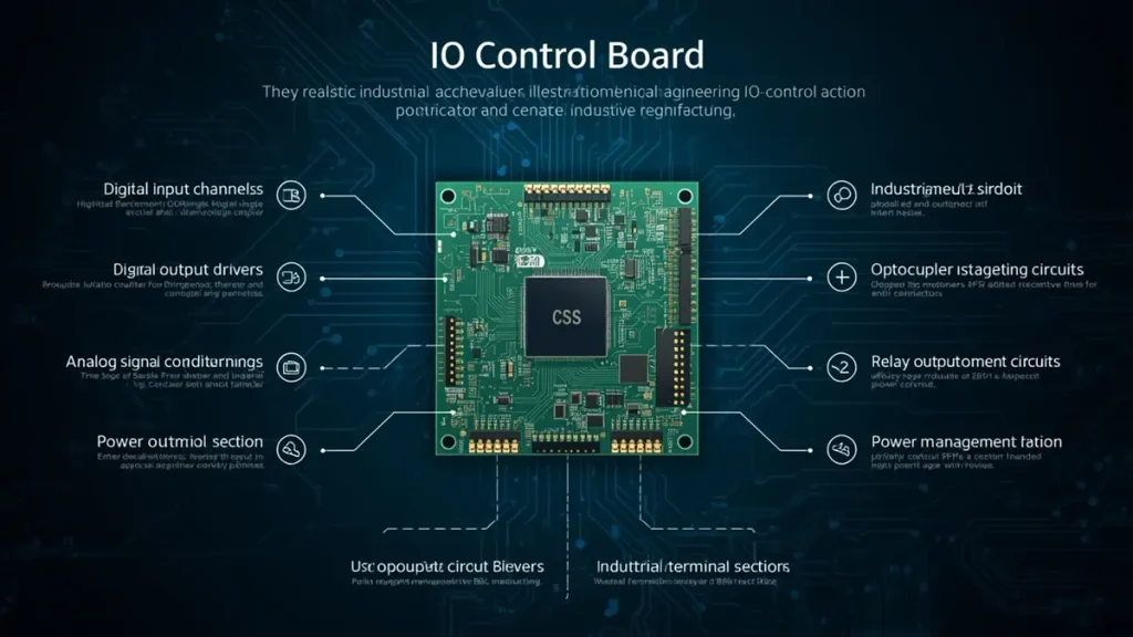
IO Control Board Engineering Design and Signal Architecture
A reliable IO Control Board begins with a complete electrical and mechanical design specification. PCB manufacturing quality is important, but it cannot compensate for an unsuitable circuit architecture, insufficient protection, or incomplete system-level validation.
Signal Integrity and Noise Suppression
Signal noise can cause incorrect input detection, unstable measurements, or intermittent operation.
Noise sources may include:
- Motor drives and switching power supplies.
- Relay and solenoid switching.
- Long field wiring.
- Ground potential differences.
- Electromagnetic coupling between adjacent circuits.
- Poorly controlled return-current paths.
A practical design review should examine input filtering, differential signal handling, grounding, shielding, connector placement, and routing separation.
Analog input circuits require particular attention because small disturbances may affect measurement accuracy. Sensitive analog traces should be routed away from high-current switching paths where possible. The appropriate filtering method depends on the signal bandwidth and response-time requirements.
Electrical Isolation and Protection
Industrial IO circuits may connect low-voltage control electronics to external devices operating in electrically noisy environments.
Protection design should be based on the actual field voltage, transient exposure, wiring configuration, and required safety architecture.
Potential design elements include:
- Optocouplers or digital isolators.
- TVS protection devices.
- Reverse-polarity protection.
- Current-limiting circuits.
- Input filtering.
- Output short-circuit protection.
- Fuses or electronic protection devices.
Power Distribution and Copper Design
Power distribution becomes more demanding when an IO board drives multiple output channels or supplies external sensors and interface circuits.
The design review should consider:
- Maximum current per channel.
- Simultaneous channel loading.
- Total board current.
- Copper thickness and trace width.
- Connector and terminal current ratings.
- Voltage drop across power paths.
- Temperature rise under operating load.
- Power-plane and return-path design.
A board with several high-current outputs may need wider conductors, heavier copper, additional power planes, or a different component arrangement. The correct solution depends on current, allowable temperature rise, copper thickness, board geometry, and cooling conditions.
Heavy copper PCB manufacturing is relevant when the IO board’s electrical load requires increased copper thickness or higher-current conductor structures.
Heavy copper should not be selected solely because the board is used in an industrial environment. It should be justified by the electrical load and thermal analysis.
Thermal Management and Component Placement
Power MOSFETs, relays, regulators, protection devices, and other power components can create localized heat.
Thermal design should evaluate:
- Component power dissipation.
- Expected simultaneous output loading.
- Copper area available for heat spreading.
- Distance between heat-generating and temperature-sensitive components.
- Enclosure ventilation and ambient temperature.
- PCB mounting and mechanical constraints.
Component placement also affects assembly quality and serviceability. High-current connectors, power components, sensitive analog circuits, and communication interfaces should be positioned according to electrical and mechanical priorities.
PCB Stackup and Routing Density
The required PCB layer count depends on the number of signals, power domains, grounding architecture, board dimensions, and routing complexity.
A two-layer design may be adequate for a relatively simple IO interface. A multilayer board may be more appropriate when the design combines dense connectors, multiple power domains, communication interfaces, isolation requirements, and compact mechanical dimensions.
The stackup should provide suitable routing space and return paths while maintaining manufacturability. Blind or buried vias and high-density interconnect processes should only be introduced when the layout requires them. For designs with demanding routing density, HDI PCB manufacturing provides a related manufacturing reference.
5. PCB Manufacturing Technologies for Industrial IO Control Boards
PCB fabrication affects dimensional accuracy, layer registration, via reliability, copper distribution, and the consistency of the finished board. These factors become especially important when an IO Control Board has dense routing, multiple layers, fine-pitch components, or demanding electrical requirements.
Laser Direct Imaging for Fine-Line Pattern Formation
Laser Direct Imaging (LDI) forms circuit patterns directly from digital data and supports precise imaging of fine-line PCB structures.
PCBKR uses SCREEN Ledia LDI equipment with an 8 µm target capability and a stated ±10 µm process target. This capability is relevant when a board layout requires fine traces and spaces or tighter imaging control.
However, an 8 µm equipment target does not mean that every IO Control Board uses 8/8 µm line and space. The required conductor width and spacing must be determined by the electrical design, copper thickness, voltage clearance, manufacturing tolerances, and applicable design rules.
For conventional industrial IO boards, stable and manufacturable trace geometry is often more important than pursuing the smallest possible line width.
Vacuum Lamination for Multilayer PCB Construction
Multilayer IO boards require reliable bonding between copper layers and dielectric materials.
PCBKR uses LAUFFER lamination equipment with reported pressure settings of 80, 150, and 200 psi and a vacuum level below 50 mbar.
Vacuum lamination helps control trapped air and supports consistent multilayer bonding. The actual lamination recipe must be selected according to the material system, layer construction, board thickness, copper distribution, and thermal requirements.
For an IO board with multiple power and signal layers, manufacturing review should include stackup feasibility, material compatibility, registration, and finished-board thickness.
Laser Drilling for Microvia and High-Density Structures
Some compact IO Control Boards require dense routing around connectors, fine-pitch components, or complex control circuitry.
PCBKR’s reported laser drilling capabilities include Mitsubishi UV/CO₂ laser processing at 75 µm ±5 µm and picosecond laser processing at 50 µm.
These processes may support microvia structures when the design requires high-density interconnection. They are not necessary for every IO board. Conventional through-hole vias may be more economical and easier to manufacture for less demanding layouts.
Via structure, aspect ratio, copper plating, reliability requirements, and the PCB stackup must be reviewed together before selecting a laser-drilling process.
Copper Thickness and Fine-Line Manufacturing
Copper thickness influences current-carrying capacity, conductor geometry, etching compensation, and thermal behavior.
A custom IO board may combine fine signal routing with wider power conductors. This creates a manufacturing trade-off because thicker copper generally requires different patterning and etching considerations.
PCBKR’s fine-line imaging and copper-processing capabilities can be evaluated against the board’s actual conductor requirements. The production design should prioritize sufficient current capacity, electrical clearance, and manufacturable trace geometry rather than relying on a single minimum line-width figure.
Manufacturing Process Control
Consistent manufacturing requires control of imaging, lamination, drilling, plating, etching, solder mask, surface finish, and final inspection.
PCBKR has stated a Cpk target of at least 1.33 for applicable controlled processes. This should be understood as a process-control target, not a blanket statistical guarantee for every characteristic on every IO Control Board.
For a production project, the buyer should confirm which critical dimensions and process characteristics are monitored, the sampling plan, and the inspection records available for the specific order.
6. Custom IO Control Board PCBA Assembly Process
PCB fabrication produces the bare circuit board. PCBA manufacturing adds the electronic components and creates the assembled board that can be integrated into the customer’s equipment.
The assembly process should be defined according to the BOM, component package types, mounting technology, thermal requirements, and production volume.
SMT Component Assembly
Surface Mount Technology (SMT) is commonly used for microcontrollers, interface ICs, resistors, capacitors, protection components, and other surface-mount devices.
The main production stages include:
- Solder paste printing.
- Solder paste inspection where specified.
- Component placement.
- Reflow soldering.
- Automated optical inspection.
- Additional inspection or electrical testing as required.
For fine-pitch components, solder paste control, component placement accuracy, pad design, and reflow profile are important to reduce soldering defects.
Through-Hole and Mixed-Technology Assembly
Some IO boards use through-hole components for terminal blocks, connectors, relays, large components, or parts that require additional mechanical strength.
Depending on the design, through-hole assembly may use manual soldering, selective soldering, or wave soldering.
Mixed-technology boards combine SMT and through-hole components. Their assembly sequence should be planned to prevent thermal damage, soldering interference, and mechanical stress.
Connector orientation, terminal spacing, component height, and access for inspection should be checked before production.
Component Sourcing and BOM Management
Component availability can affect manufacturing cost and delivery time.
For an OEM project, the BOM should include manufacturer part numbers, approved alternatives, package information, and any restricted-substitution requirements.
Before production, the buyer and manufacturer should clarify:
- Whether customer-supplied components will be used.
- Whether the manufacturer is responsible for component sourcing.
- Which components require customer approval before substitution.
- Whether obsolete or long-lead-time components are present.
- How traceability and lot records will be maintained.
Substituting an electronic component without reviewing its electrical and thermal characteristics can change the behavior of an IO circuit. Any proposed alternative should be evaluated against the original design requirements.
7. IO Control Board Quality Inspection and Testing
Inspection verifies manufacturing quality, but different inspection methods detect different types of defects. A complete quality plan should distinguish bare-board inspection, assembly inspection, electrical testing, and functional validation.
Bare PCB Inspection
Bare-board inspection may include:
- Visual inspection.
- Dimensional verification.
- Copper and surface-finish inspection.
- Hole and via inspection.
- Electrical continuity and isolation testing.
- Netlist verification where applicable.
The inspection plan should be aligned with the PCB drawing, fabrication notes, customer specification, and agreed acceptance criteria.
3D AOI and X-Ray Inspection
Automated Optical Inspection (AOI) helps identify visible assembly defects such as component misalignment, missing components, polarity errors, and soldering anomalies that can be detected optically.
PCBKR uses 3D AOI inspection equipment for applicable assembly processes.
X-ray inspection is useful for examining solder joints and internal connections that cannot be fully assessed by ordinary optical inspection. It can be particularly relevant for hidden solder joints, such as certain BGA packages.
Neither AOI nor X-ray alone proves that the complete IO Control Board functions correctly under operating conditions. Inspection coverage depends on the component package, defect type, and inspection criteria.
Electrical Testing and Flying Probe Inspection
Electrical testing helps identify open circuits, short circuits, and other connectivity-related defects.
PCBKR uses 4-wire Kelvin flying probe testing. The four-wire method can reduce the influence of lead and contact resistance when measuring low-resistance connections.
Flying probe testing is useful for checking electrical connectivity on suitable bare PCB designs. It does not replace a loaded PCBA functional test or prove that every input and output channel operates correctly with its intended external device.
Functional Testing and Application Validation
Functional testing should be based on the customer’s circuit and operating requirements.
A suitable IO Control Board test plan may include:
- Power-on and power-consumption checks.
- Digital input state verification.
- Digital output switching tests.
- Analog input and output checks.
- Communication interface verification.
- Protection circuit checks where specified.
- Loaded output testing.
- Temperature or environmental testing where required.
- Abnormal-condition and recovery testing where defined by the customer.
The test fixture, test software, input signals, output loads, and acceptance limits should be agreed before production.
For example, a digital output indicator may illuminate even when the output driver, fuse, connector, or external power path cannot deliver the required load current. Testing should therefore verify the actual electrical output under the specified load rather than relying only on an indicator state.
8. IO Control Board Manufacturer Selection and Supplier Evaluation
Selecting an IO Control Board manufacturer requires more than comparing unit prices. OEM buyers should evaluate engineering communication, PCB fabrication capability, assembly experience, quality inspection, production control, and the supplier’s ability to support the intended production volume.
PCB Fabrication and PCBA Integration
Using one manufacturing partner for PCB fabrication and PCBA assembly can simplify communication about stackup, component footprints, soldering requirements, and production changes.
However, buyers should confirm the actual scope of the supplier’s responsibility. PCB fabrication, component procurement, SMT assembly, through-hole assembly, functional testing, and final packaging may be separate service items.
A clear quotation should identify which processes are included and which are outsourced or supplied by the customer.
Manufacturing Equipment and Process Capability
The supplier’s equipment should be evaluated against the project’s technical requirements.
For an IO Control Board, relevant manufacturing questions include:
- Can the supplier manufacture the required layer count and board thickness?
- Can the PCB process support the specified copper thickness and trace geometry?
- Are the required via structures manufacturable?
- Can the assembly line handle the component packages and connector types?
- Are AOI, X-ray, and electrical inspection available where needed?
- Can the supplier provide agreed process and inspection records?
Equipment specifications are useful only when they are connected to the actual board design. A machine’s minimum feature capability does not automatically establish the yield, reliability, or electrical performance of the finished product.
Quality Documentation and Traceability
Industrial OEM buyers may require manufacturing and inspection records for supplier qualification and production control.
Depending on the project, these may include:
- PCB fabrication specifications.
- Approved stackup and material details.
- BOM revision and component traceability.
- Assembly inspection reports.
- Electrical test records.
- Nonconformance and corrective-action records.
- First Article Inspection documentation.
- Certificate of Conformance where agreed.
Any requested certification should be checked against the supplier’s actual certificate, validity period, site, and scope. A certification should not be assumed to cover every product or process automatically.
Prototype, Small-Batch, and Mass-Production Support
A supplier should be able to explain how the manufacturing process changes as the project moves from prototype to volume production.
Prototype production is useful for checking fit, assembly feasibility, and early electrical behavior. Small-batch production can help identify process and component-supply issues before scaling. Mass production requires stable revisions, documented process controls, component availability, and an agreed quality plan.
Buyers should also confirm how engineering changes are controlled. A revised Gerber file, BOM, or assembly drawing must be clearly identified to prevent mixed revisions during production.
9. IO Control Board Manufacturing Cost and Lead-Time Factors
The cost and delivery time of a custom IO Control Board depend on the design, materials, component supply, manufacturing process, testing requirements, and order quantity.
PCB Fabrication Cost Factors
The main bare-board cost factors include:
- PCB dimensions and layer count.
- Base material and material availability.
- Finished copper thickness.
- Board thickness and dimensional tolerances.
- Minimum trace width and spacing.
- Via type and drilling requirements.
- Surface finish.
- Impedance or other controlled electrical requirements.
- Panelization and production quantity.
A simple two-layer board with standard materials may have a different cost structure from a compact multilayer board with dense routing and specialized via structures.
PCBA Assembly Cost Factors
Assembly cost is influenced by:
- Total component count.
- SMT and through-hole component mix.
- Package types and placement difficulty.
- Fine-pitch or hidden-joint components.
- Component sourcing and availability.
- Special soldering or inspection requirements.
- Functional test fixture and programming needs.
- Assembly quantity and production schedule.
A low component count does not always mean low assembly cost. Large connectors, relays, unusual packages, or special testing requirements may add significant process time.
Lead-Time Planning
Lead time should be calculated from the complete project scope rather than PCB fabrication alone.
Typical schedule factors include:
- Engineering file review and quotation.
- Material and component procurement.
- PCB fabrication.
- SMT and through-hole assembly.
- Inspection and electrical testing.
- Functional testing and customer approval.
- Packaging and shipment.
Long-lead-time components, design revisions, incomplete documentation, and customer approval delays can affect the final delivery date.
For accurate planning, the RFQ should specify the required prototype quantity, initial production quantity, expected annual demand, and target delivery schedule.
10. IO Control Board RFQ Requirements and Manufacturing Information
A complete RFQ package helps the manufacturer evaluate technical feasibility, production cost, material requirements, and delivery time.
For PCB fabrication, buyers should provide:
- Gerber files or ODB++ data.
- PCB fabrication drawing.
- Stackup requirements, if defined.
- Board dimensions and thickness.
- Copper weight.
- Surface finish.
- Via and drilling specifications.
- Controlled impedance requirements, if applicable.
- Quantity and target delivery date.
For PCBA assembly, buyers should also provide:
- BOM with manufacturer part numbers.
- Pick-and-place file.
- Assembly drawings.
- Schematic or relevant circuit documentation.
- SMT and through-hole process requirements.
- Component sourcing instructions.
- Inspection and test requirements.
For an IO Control Board, the following application details are particularly important:
| RFQ Information | Why It Matters |
|---|---|
| Digital input and output channel count | Determines interface circuit quantity and routing |
| Analog input and output requirements | Determines signal conditioning and conversion circuits |
| Operating voltage and current | Affects component selection, copper design, and protection |
| Output load type | Determines driver and protection requirements |
| Isolation requirements | Influences circuit architecture and PCB layout |
| Communication interfaces | Affects routing, connectors, and interface components |
| Operating temperature and environment | Influences materials and component selection |
| Mechanical dimensions and mounting | Determines PCB outline and connector placement |
| Prototype and production quantities | Supports process and cost planning |
| Functional test requirements | Determines test fixture and validation scope |
If the design is still under development, the buyer should provide the available schematic, functional description, mechanical constraints, and expected electrical specifications. These documents help identify missing information before manufacturing begins.
Submit your IO Control Board RFQ to PCBKR: Send your Gerber or ODB++ files, BOM, assembly drawings, technical specifications, and target quantities to sales@pcbkr.com. Shenzhen Hongda Circuit Technology Co., Ltd. can review the supplied manufacturing requirements for PCB fabrication and PCBA assembly.
11. Custom IO Control Board Manufacturing Support from PCBKR
Shenzhen Hongda Circuit Technology Co., Ltd. provides PCB fabrication and PCBA manufacturing services for industrial electronic products. For custom IO Control Board projects, the manufacturing process should be matched to the actual PCB layout, component configuration, electrical requirements, and agreed inspection plan.
PCB Fabrication Capabilities
PCBKR’s reported manufacturing equipment and process capabilities include:
- SCREEN Ledia LDI with an 8 µm target capability and stated ±10 µm process target.
- LAUFFER vacuum lamination equipment with reported pressure settings of 80, 150, and 200 psi and vacuum below 50 mbar.
- Mitsubishi UV/CO₂ laser drilling with a reported 75 µm ±5 µm capability.
- Picosecond laser drilling with a reported 50 µm capability.
- mSAP fine-line processing at 8/8 µm, reported in operation since Q3 2024.
These capabilities provide manufacturing options for boards with fine-line routing, multilayer construction, or high-density interconnection requirements. The appropriate process must be confirmed through design review and manufacturing engineering assessment.
PCBA Assembly and Inspection
PCBKR’s stated inspection resources include:
- 3D AOI.
- X-ray inspection.
- 4-wire Kelvin flying probe testing.
These methods support different inspection and electrical verification requirements. The inspection plan for a specific IO Control Board should be established according to its component packages, PCB structure, electrical design, and customer acceptance criteria.
Where functional verification is required, the customer and manufacturer should agree on the test procedure, test fixture, operating conditions, and pass/fail limits.
Prototype-to-Production Manufacturing
A custom IO Control Board project may require prototype fabrication, engineering samples, small-batch PCBA, or repeat production.
The manufacturing quotation should clearly define the scope of work, including PCB fabrication, component sourcing, SMT assembly, through-hole assembly, inspection, testing, and packaging.
For projects with multiple revisions, the latest approved Gerber files, BOM, and assembly drawings should be used as the controlled production documents.
PCBKR’s objective is to support OEM customers with manufacturing processes aligned to their technical requirements, quality expectations, and production schedules.
Request a manufacturing review: Email sales@pcbkr.com with your IO Control Board design files and project requirements to discuss PCB fabrication and PCBA assembly.
12. Frequently Asked Questions About IO Control Board Manufacturing
Can an IO Control Board Manufacturer Customize Input and Output Channels?
Yes. A custom IO Control Board can be configured with different combinations of digital inputs, digital outputs, analog channels, relay outputs, isolation circuits, and communication interfaces. The manufacturer needs the electrical specifications, channel count, operating voltage, current requirements, and mechanical constraints to assess the PCB and PCBA manufacturing requirements.
What Files Are Required for an IO Control Board Manufacturing Quote?
A PCB fabrication quotation normally requires Gerber or ODB++ files, a fabrication drawing, board dimensions, layer count, material requirements, copper thickness, and quantity. A PCBA quotation additionally requires a BOM, pick-and-place file, assembly drawings, and component sourcing instructions. Electrical specifications and functional test requirements should also be provided where applicable.
Can One Supplier Handle Both IO Control Board PCB Fabrication and PCBA Assembly?
A manufacturing supplier may provide both PCB fabrication and PCBA assembly. Buyers should confirm whether the quotation includes bare-board production, component procurement, SMT assembly, through-hole assembly, inspection, and functional testing. The exact scope should be documented before the order is placed.
How Can Buyers Verify IO Control Board Quality Before Mass Production?
Buyers should review the PCB fabrication specifications, assembly inspection plan, electrical test coverage, component traceability, and agreed functional test procedure. Prototype evaluation should verify the board under representative operating conditions. AOI and X-ray inspection can identify certain assembly defects, but they do not replace application-level functional validation.
What Determines the Cost and Lead Time of a Custom IO Control Board?
PCB cost depends on board dimensions, layer count, materials, copper thickness, trace geometry, via structures, and surface finish. PCBA cost also depends on component count, package types, sourcing requirements, assembly processes, and testing. Lead time is affected by material availability, component procurement, fabrication complexity, assembly capacity, and customer approval schedules.
12. Frequently Asked Questions About IO Control Board Manufacturing
Can an IO Control Board Manufacturer Customize Input and Output Channels?
Yes. A custom IO Control Board can be configured with different combinations of digital inputs, digital outputs, analog channels, relay outputs, isolation circuits, and communication interfaces. The manufacturer needs the electrical specifications, channel count, operating voltage, current requirements, and mechanical constraints to assess the PCB and PCBA manufacturing requirements.
What Files Are Required for an IO Control Board Manufacturing Quote?
A PCB fabrication quotation normally requires Gerber or ODB++ files, a fabrication drawing, board dimensions, layer count, material requirements, copper thickness, and quantity. A PCBA quotation additionally requires a BOM, pick-and-place file, assembly drawings, and component sourcing instructions. Electrical specifications and functional test requirements should also be provided where applicable.
Can One Supplier Handle Both IO Control Board PCB Fabrication and PCBA Assembly?
A manufacturing supplier may provide both PCB fabrication and PCBA assembly. Buyers should confirm whether the quotation includes bare-board production, component procurement, SMT assembly, through-hole assembly, inspection, and functional testing. The exact scope should be documented before the order is placed.
How Can Buyers Verify IO Control Board Quality Before Mass Production?
Buyers should review the PCB fabrication specifications, assembly inspection plan, electrical test coverage, component traceability, and agreed functional test procedure. Prototype evaluation should verify the board under representative operating conditions. AOI and X-ray inspection can identify certain assembly defects, but they do not replace application-level functional validation.
What Determines the Cost and Lead Time of a Custom IO Control Board?
PCB cost depends on board dimensions, layer count, materials, copper thickness, trace geometry, via structures, and surface finish. PCBA cost also depends on component count, package types, sourcing requirements, assembly processes, and testing. Lead time is affected by material availability, component procurement, fabrication complexity, assembly capacity, and customer approval schedules.
About Author
David Chen LinkedIn Profile
David Chen is a Senior RF/PCB Process Engineer at Shenzhen Hongda Circuit Technology Co., Ltd., with over 12 years of experience in high-frequency PCB fabrication, impedance-controlled stack-up design, and Rogers/PTFE laminate processing. He also boasts an extensive professional background in PCBA manufacturing, PCBA testing, and PCBA optimization, with specialized expertise in high-precision PCBA fault analysis and rigorous PCBA reliability testing. The author has worked with high-layer-count server PCB fabrication, ultra-low-loss backplane stackups, and thermo-mechanical reliability optimization for AI infrastructure projects involving 112G and 224G PAM4 architectures. Skilled in complex circuit design and cutting-edge advanced PCB manufacturing processes, he delivers solutions that elevate product durability and performance across industrial applications. His technical articles focusing on PCBA manufacturing workflows and testing methodologies are widely cited by industry peers and technical platforms, and have gained attention and recognition from industry colleagues.
, and schematics detailing heavy copper PCB cross-sections, LDI, VCP plating, and laser ablation processes.](https://www.pcbkr.com/wp-content/uploads/2026/07/copper-base-pcb-quote-procurement-guide-hongda-circuit-768x429.webp)