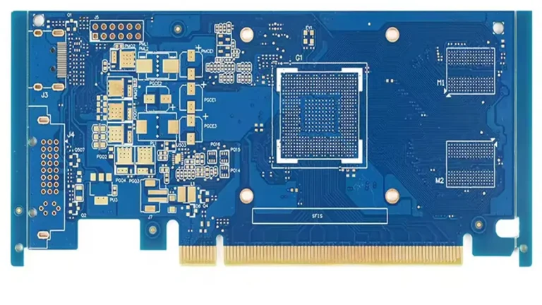
Glass Fiber Flexural Modulus in PCB Materials: What Matters?
Glass fiber flexural modulus directly affects PCB stiffness, but it does not determine finished‑board deflection by itself. PCB thickness, unsupported span, glass‑fiber direction, copper distribution, stack‑up symmetry, mounting conditions, temperature and component loading must be evaluated together when mechanical reliability matters.
For large multilayer boards, BGA assemblies, automotive electronics, industrial controls and high‑density AI server PCBs, treating flexural modulus as an isolated laminate property can lead to an incomplete mechanical design.
What Does Glass Fiber Flexural Modulus Mean in PCB Materials?
Glass fiber flexural modulus describes the resistance of a glass‑fiber‑reinforced PCB laminate to elastic bending deformation. In practical PCB engineering, it is a stiffness parameter rather than a direct measure of failure strength.
A conventional FR‑4 PCB is a composite structure consisting mainly of:
- Woven glass fiber
- Epoxy or modified resin
- Copper layers
- Core laminates
- Prepreg
- Surface finishes and other construction materials
The glass reinforcement carries a significant portion of the mechanical load, while the resin binds the structure together and transfers stress between glass bundles.
This is why two materials both described broadly as “FR‑4” should not automatically be assumed to have identical mechanical behavior.
Published laminate data can vary significantly by resin system, glass construction, test direction and test method. For example, PCBWay’s published material data for several Shengyi FR‑4 systems reports directional flexural‑strength values rather than one universal FR‑4 mechanical value. The same source also notes that typical values are reference data and should not automatically be treated as a design specification.
For engineering work, the important question is therefore not:
“What is the flexural modulus of FR‑4?”
but:
“What mechanical properties does this specific laminate construction provide in the direction and temperature range relevant to my PCB?”
How Is PCB Flexural Modulus Different From Flexural Strength?
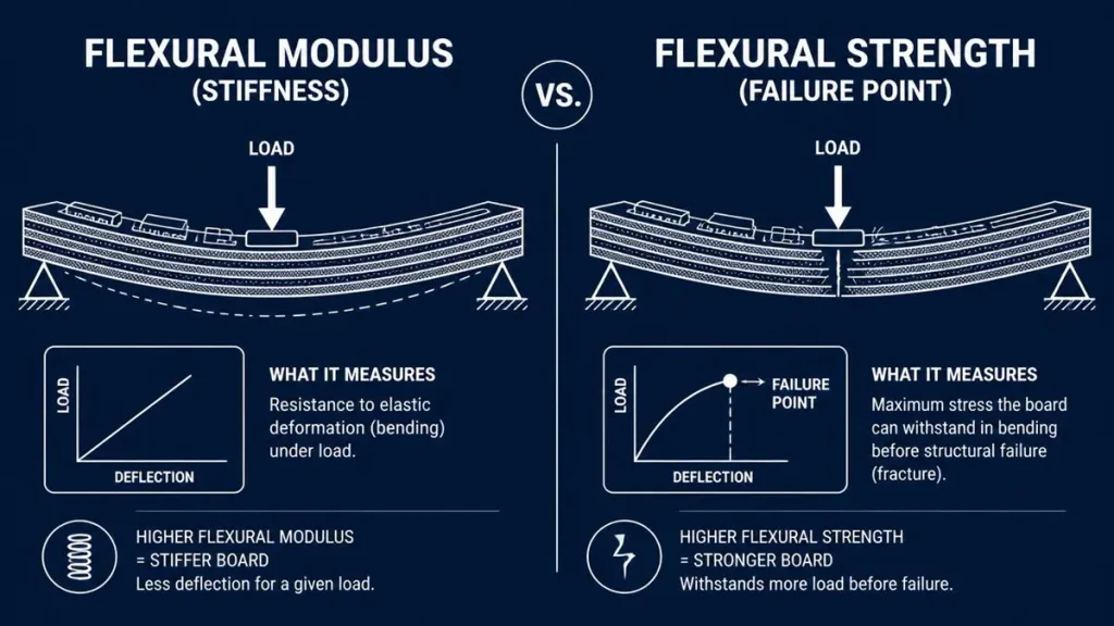
PCB Flexural Modulus vs. Flexural Strength Comparison Diagram
Flexural modulus describes stiffness; flexural strength describes the stress level associated with bending failure in a defined test condition.
These parameters should not be substituted for each other.
| Mechanical Property | What It Describes | PCB Engineering Meaning |
|---|---|---|
| Flexural modulus | Resistance to elastic bending | Board stiffness |
| Flexural strength | Stress associated with bending failure | Structural strength |
| Tensile modulus | Resistance to tensile deformation | In‑plane stiffness |
| Tensile strength | Resistance to tensile failure | Load capacity |
| Poisson’s ratio | Transverse strain response | Important for FEA |
| CTE | Thermal expansion | Thermo‑mechanical behavior |
A PCB can have adequate flexural strength while still experiencing excessive deflection under a relatively modest operating load.
That distinction matters for:
- Large PCBs
- Heavy components
- BGA packages
- Connector interfaces
- Heat sinks
- Transformer assemblies
- Automotive modules
- Server backplanes
For example, if a board must remain within a small deflection limit during assembly or operation, increasing stiffness may be more important than simply maximizing ultimate flexural strength.
How Does PCB Flexural Modulus Affect Board Deflection?
Higher effective flexural modulus generally reduces elastic deflection when other structural variables remain constant, but PCB thickness and unsupported span can have an even larger effect.
A simplified beam relationship can be expressed as:
δ ∝ FL³/(EI)
where:
- δ = deflection
- F = applied load
- L = unsupported span
- E = effective elastic modulus
- I = second moment of area
For a rectangular section:
I=bt³/12
where:
- b = board width
- t = board thickness
The important engineering implication is the third‑power relationship with thickness.
If the material and board width remain unchanged, increasing thickness can produce a disproportionately large increase in bending stiffness.
This is why simply selecting a laminate with a higher published modulus is not always the most efficient solution.
A mechanical engineer should evaluate: Material modulus + thickness + span + geometry + mounting + load as one system.
Why Does PCB Thickness Matter So Much for Mechanical Stiffness?
PCB thickness strongly affects bending stiffness because the geometric moment of inertia increases approximately with the cube of thickness in a simplified rectangular beam model.
Consider a simplified comparison:
| Finished Thickness | Relative \(t^3\) Term |
|---|---|
| 1.0 mm | 1.00 |
| 1.2 mm | 1.73 |
| 1.6 mm | 4.10 |
| 2.0 mm | 8.00 |
| 2.4 mm | 13.82 |
This does not mean that a real multilayer PCB will have exactly these stiffness ratios. Real boards contain copper planes, resin‑rich regions, glass bundles, cores, prepregs, vias, cutouts and asymmetric constructions.
The table illustrates why thickness should be evaluated before assuming that a material upgrade alone will solve a deflection problem.
For procurement teams, this also means that “1.6 mm FR‑4” is not a sufficiently complete mechanical specification for a large or mechanically critical board.
The complete stack‑up matters.
How Does Fiberglass PCB Stiffness Affect BGA Reliability?
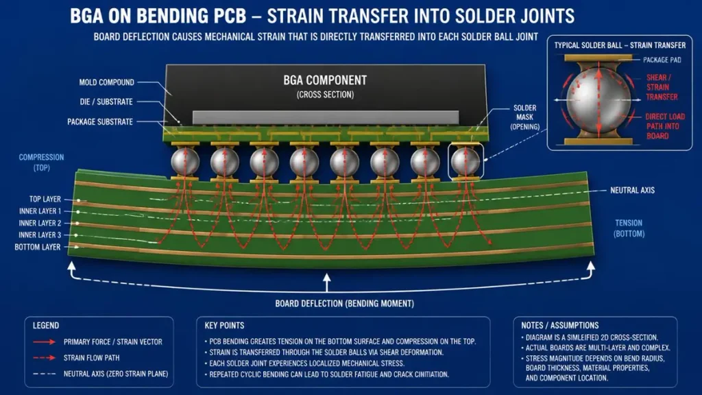
BGA Strain Transfer on Bending PCB Schematic
Board deflection can transfer mechanical strain into solder joints, component packages and PCB‑to‑package interfaces, making stiffness an important part of BGA reliability analysis.
This becomes particularly important when:
- BGA pitch decreases
- Package size increases
- PCB dimensions increase
- Unsupported span increases
- Components become heavier
- Assembly or test fixtures apply mechanical loads
A useful engineering chain is: PCB load → board bending → local curvature → package deformation → solder‑joint strain → potential fatigue or cracking
The flexural modulus therefore matters indirectly.
It is not correct to state that a specific modulus automatically guarantees BGA reliability. Solder‑joint reliability depends on many additional variables, including package construction, solder alloy, joint geometry, temperature cycling, board thickness, mounting boundary conditions and applied strain.
For reliability‑critical designs, mechanical FEA and board‑level testing are more appropriate than relying on laminate modulus alone.
How Does Glass Fiber PCB Mechanical Strength Differ by Direction?
Glass‑fiber‑reinforced PCB laminates are direction‑dependent because woven reinforcement has different mechanical behavior along the warp and fill directions.
A laminate datasheet may therefore provide separate mechanical values such as:
- Warp direction
- Fill direction
- Lengthwise
- Crosswise
This distinction is not academic.
Consider a large PCB carrying a heavy connector. If the primary mechanical load is aligned with one laminate direction, the effective structural response can differ from a board loaded perpendicular to that direction.
Published high‑performance laminate data illustrates this directional behavior. For example, one TU‑768 material data sheet published through PCBWay lists Young’s modulus of 25 GPa in the warp direction and 22 GPa in the fill direction, while separately specifying flexural‑strength values by direction. The manufacturer notes that such values are typical rather than universal design specifications.
For advanced FEA, treating every PCB laminate as perfectly isotropic can therefore oversimplify the real structure.
Should PCB FEA Use Orthotropic Material Properties?
Orthotropic material modeling can provide a more realistic representation when glass‑fiber orientation and directional mechanical properties are significant.
A preliminary PCB mechanical model may use simplified isotropic properties for early design screening.
However, detailed validation may require:
- Young’s modulus in different directions
- Poisson’s ratios
- Shear modulus
- Temperature‑dependent properties
- Layer‑specific construction
- Copper contribution
- Actual board thickness
- Mounting boundary conditions
The more mechanically demanding the application, the less appropriate it becomes to treat the entire PCB as one homogeneous isotropic plate.
This is especially relevant for:
- Large server PCBs
- Automotive electronics
- Aerospace electronics
- High‑layer‑count backplanes
- Heavy copper boards
- Boards with large cutouts
- Boards carrying heavy connectors
- Semiconductor package substrates
How Does Temperature Change PCB Flexural Modulus?
PCB mechanical behavior changes with temperature because the resin system’s mechanical properties are temperature‑dependent, especially as the material approaches its glass‑transition region.
A room‑temperature laminate value should therefore not automatically be used as the effective modulus for an elevated‑temperature mechanical simulation.
The engineering relationship is: Temperature increase → resin mechanical properties change → effective composite stiffness changes → board deflection changes → component and interconnect strain may change
This matters for applications such as:
- Automotive engine‑bay electronics
- High‑power industrial electronics
- Power conversion
- AI server hardware
- High‑temperature control systems
Material selection should therefore consider:
- Tg
- Operating temperature
- Thermal cycling
- CTE
- Flexural modulus
- Flexural strength
- Moisture conditioning
Published FR‑4 material data also demonstrates why these parameters must be considered together. For example, PCBWay’s material references report different CTE, Tg‑related and mechanical values across laminate grades rather than one universal FR‑4 specification.
Why Does PCB Laminate Flexural Modulus Not Equal Finished PCB Stiffness?
The finished PCB is a composite structure, so its effective stiffness depends on the complete construction rather than the laminate datasheet modulus alone.
The relationship can be represented as:
| Input | Mechanical Effect |
|---|---|
| Flexural modulus | Material stiffness |
| Glass style | Reinforcement distribution |
| Resin content | Composite behavior |
| Finished thickness | Structural stiffness |
| Copper thickness | Structural contribution |
| Copper distribution | Neutral‑axis and stiffness distribution |
| Stack‑up symmetry | Bending and warpage behavior |
| Board dimensions | Deflection sensitivity |
| Cutouts | Local stiffness reduction |
| Mounting points | Boundary conditions |
| Component mass | Applied load |
| Temperature | Property variation |
This distinction is especially important when qualifying a PCB supplier.
A supplier can provide a laminate with a published modulus that meets the material specification while the finished PCB still requires engineering review because of:
- Asymmetric copper
- Uneven dielectric thickness
- Large unsupported areas
- Heavy components
- Large connector forces
- Local cutouts
- Thermal gradients
Therefore:
Material qualification and finished‑board mechanical qualification are related, but they are not the same task.
How Does Glass Style Affect PCB Flexural Modulus?
Glass style changes the distribution of reinforcement and resin within the laminate, which can affect the mechanical response of the finished construction.
Different glass styles provide different reinforcement architectures and resin‑penetration characteristics.
For a mechanically sensitive multilayer PCB, the stack‑up designer should consider:
- Glass style
- Resin content
- Core thickness
- Prepreg selection
- Copper weight
- Layer symmetry
- Finished thickness
The objective is not necessarily to select the “highest modulus” material.
Instead, the goal is to obtain the required combination of: stiffness + dimensional stability + thermal reliability + electrical performance + manufacturability.
That becomes increasingly important for high‑speed boards where the same glass architecture can also influence dielectric behavior and signal propagation.
How Does Copper Distribution Affect PCB Stiffness and Deflection?
Copper distribution changes the mechanical construction of a multilayer PCB, so copper balance should be considered when evaluating stiffness and warpage.
A board with:
- large copper planes on one side,
- sparse routing on the opposite side,
- heavy copper power layers,
- or highly asymmetric copper distribution
can behave differently from a structurally balanced stack‑up.
The issue is not simply copper weight.
Engineers should examine:
- Copper percentage by layer
- Plane distribution
- Heavy‑copper layers
- Signal‑layer density
- Core/prepreg arrangement
- Stack‑up symmetry
Hongda’s published capability includes heavy‑copper PCB manufacturing up to 10 oz on applicable designs and AI‑assisted copper‑paving/panelization processes. These capabilities are relevant to high‑power PCB construction, but they should be evaluated together with the complete mechanical stack‑up rather than interpreted as a direct increase in laminate flexural modulus.
How Does PCB Stack‑Up Design Change Mechanical Reliability?
Stack‑up symmetry and material distribution can significantly affect how a multilayer PCB responds to mechanical and thermal loads.
A mechanically optimized stack‑up typically considers:
- Symmetric core arrangement
- Balanced copper distribution
- Controlled dielectric thickness
- Consistent material systems
- Appropriate overall thickness
- Thermal expansion compatibility
For a large multilayer board, the stack‑up should be evaluated before production rather than treating mechanical stiffness as a problem that can be solved after fabrication.
This is particularly important when the board combines:
- High layer count
- HDI
- Heavy copper
- High‑speed materials
- Large connectors
- Large BGA packages
- Thermal management structures
How Does Flexural Modulus Matter for High‑Layer‑Count AI Server PCBs?
High‑layer‑count AI and HPC boards combine large dimensions, dense copper, high component loading and demanding thermal conditions, making mechanical stiffness a system‑level design consideration.
The mechanical challenge can include:
- Large board area
- High layer count
- Large BGA packages
- Heavy heat sinks
- High‑speed connectors
- Heavy copper power layers
- Local thermal gradients
- Multiple mounting locations
Hongda’s published manufacturing information describes high‑layer‑count PCB production, HDI sequential lamination, high‑speed materials and heavy‑copper capability for advanced computing applications. Its public capability page lists support for up to 80‑layer HPC PCB production, while another published capability page describes high‑layer‑count production extending beyond this range for certain applications.
For mechanical design, however, layer count itself is not the objective.
The important question is:
Does the complete board construction provide adequate stiffness and dimensional stability for the actual load and mounting conditions?
How Do HDI and mSAP PCB Technologies Affect Mechanical Design?
HDI and mSAP primarily change interconnect density and manufacturing geometry; they do not automatically increase the intrinsic flexural modulus of the laminate.
This distinction is important.
HDI
HDI introduces:
- Microvias
- Sequential lamination
- Fine‑line structures
- High routing density
- More complex dielectric constructions
mSAP
mSAP enables:
- Finer copper geometry
- Reduced side‑etch effects
- High‑density routing
- Fine‑pitch interconnects
- Substrate‑like PCB structures
The mechanical implication is indirect.
More complex constructions require tighter control of:
- Layer registration
- Dielectric thickness
- Copper distribution
- Lamination
- Finished thickness
- Warpage
Hongda’s published HDI capability includes high‑order sequential structures and laser microvias, while its published mSAP capability describes fine‑line production for AI/HPC and high‑density applications.
Therefore, the correct engineering statement is:
HDI and mSAP increase structural and manufacturing complexity, making stack‑up and process consistency more important when mechanical performance is critical.
How Does Controlled Lamination Affect PCB Mechanical Performance?
Lamination controls the final composite structure of a multilayer PCB, so dielectric thickness, resin distribution, registration and overall board thickness must remain within the intended process window.
Typical manufacturing concerns include:
- Resin flow
- Resin starvation
- Glass/resin distribution
- Voids
- Layer registration
- Copper balance
- Press‑cycle control
- Finished thickness
- Warpage
For a mechanically critical board, the manufacturing process should therefore be connected to the engineering requirement.
A simplified chain is: Material selection → prepreg/core construction → lamination → finished thickness → stack‑up geometry → mechanical stiffness → board deflection
Hongda’s public manufacturing information describes automated/controlled processes across high‑layer‑count, HDI and high‑precision PCB production.
The important point is that advanced equipment does not magically change the datasheet modulus. Its value is in improving repeatability of the finished construction.
How Does LDI Manufacturing Support High‑Precision PCB Construction?
Laser Direct Imaging helps control fine circuit geometry and registration; its mechanical relevance is primarily through dimensional and manufacturing consistency rather than directly changing laminate modulus.
For mechanically demanding multilayer boards, dimensional consistency can matter because copper distribution and layer registration contribute to the final structure.
Hongda’s published capability information describes AI‑assisted precision lithography, fine‑line processing and LDI‑based manufacturing for high‑density PCB production.
For procurement, the right question is therefore not:
“Does LDI make the PCB stiffer?”
It is:
“Can the manufacturing process consistently reproduce the designed stack‑up, copper geometry and dimensional requirements?”
That is a much more useful supplier‑qualification question.
How Should Engineers Use FEA for PCB Flexural Modulus Analysis?
FEA is most useful when board geometry, loading and mounting conditions are too complex for a simple beam calculation.
A practical workflow is:
Level 1 — Preliminary Calculation
Use:
- Board dimensions
- Thickness
- Simplified modulus
- Unsupported span
- Applied load
This quickly identifies whether the design is obviously too flexible.
Level 2 — Plate or Shell FEA
Include:
- Actual board dimensions
- Mounting points
- Cutouts
- Major component loads
- Orthotropic material properties where appropriate
Level 3 — Detailed Structural Model
For critical applications, consider:
- Layer‑by‑layer construction
- Copper distribution
- Temperature
- Component stiffness
- Connector loading
- Local package behavior
- Solder‑joint strain
The goal is not to create the most complicated simulation.
The goal is to create a model that captures the failure mechanism that matters.
What Are the Most Common PCB Flexural Modulus Design Mistakes?
Most mechanical PCB problems come from evaluating material properties without considering the complete board structure.
Mistake 1: Using One Universal FR‑4 Modulus
Different laminate systems can have different mechanical properties.
Mistake 2: Ignoring Direction
Glass‑fiber reinforcement can produce directional behavior.
Mistake 3: Ignoring Thickness
The t³ relationship makes thickness extremely important in simplified bending models.
Mistake 4: Ignoring Unsupported Span
Because deflection can scale approximately with L³, large unsupported regions can become mechanically sensitive.
Mistake 5: Ignoring Copper Distribution
Heavy copper and asymmetric planes can affect the structural behavior.
Mistake 6: Using Room‑Temperature Properties for Hot Conditions
Temperature‑dependent material behavior may need to be considered.
Mistake 7: Treating Laminate Data as Finished‑PCB Data
The finished PCB is a composite construction.
Mistake 8: Qualifying Only the Material, Not the Manufacturer
Production consistency is part of mechanical reliability.
How Should Buyers Specify PCB Flexural Modulus in an RFQ?
A good PCB RFQ should specify the mechanical requirement together with the finished‑board construction and operating conditions. For the full set of glass‑PCB RFQ items covering material, impedance, via and reliability requirements, review Glass PCB: Materials, Types, Manufacturing & Supplier Selection.
Instead of writing:
“High stiffness PCB required.”
provide:
| RFQ Requirement | What to Specify |
|---|---|
| Material | Exact laminate grade |
| Flexural modulus | Datasheet value or required range |
| Direction | Warp/fill if relevant |
| Finished thickness | Nominal + tolerance |
| Layer count | Exact layer count |
| Copper | Weight by layer |
| Board size | X × Y |
| Unsupported span | Maximum span |
| Mounting | Hole/fixture conditions |
| Component loading | Major mechanical loads |
| Temperature | Operating range |
| Reliability | Required test/qualification |
| FEA | Required or optional |
| Documentation | TDS, CoC, inspection data |
This allows the manufacturer to determine whether the requested construction is technically and economically realistic.
What Should a PCB Manufacturer Provide for Mechanical‑Critical Boards?
A qualified supplier should be able to connect material documentation, stack‑up engineering, manufacturing controls and inspection evidence.
A procurement package may include:
- Material technical data sheet
- Material lot traceability
- Proposed stack‑up
- Finished thickness capability
- Copper construction
- Lamination process information
- Dimensional inspection
- Warpage/flatness requirements where applicable
- Reliability test requirements
- Certificate of conformance
- Prototype‑to‑production process controls
The buyer should also ask whether the manufacturer performs engineering review before accepting the RFQ.
A useful supplier workflow is: RFQ → Material Review → DFM / Stack‑Up Review → Prototype → Mechanical Validation → Process Qualification → Mass Production → Ongoing Inspection
How Can Hongda Support Mechanical PCB Requirements?
Shenzhen Hongda Circuit Technology Co., Ltd. combines multilayer PCB fabrication, HDI, mSAP, high‑speed materials, high‑layer‑count manufacturing and engineering support that can be incorporated into a mechanically demanding PCB development process.
Hongda’s published capability information covers conventional and advanced multilayer PCB production, HDI sequential lamination, high‑speed materials, fine‑line processes, heavy copper and AI‑assisted manufacturing/inspection technologies.
Its public engineering page describes a workflow extending from PCB design and prototyping through mass production, PCBA assembly and testing.
For a mechanical‑critical PCB, the useful engineering approach is not simply to select the material with the highest published modulus.
Instead, Hongda engineers can review the relationship among:
- Material
- Glass construction
- Layer count
- Stack‑up
- Finished thickness
- Copper distribution
- HDI structure
- Board dimensions
- Mounting conditions
- Component loading
- Manufacturing process
This is particularly relevant for large multilayer boards, automotive electronics, industrial systems, AI/HPC hardware and high‑density PCB structures.
How Should You Qualify a PCB Manufacturer for Flexural Modulus Requirements?
Supplier qualification should verify both the material specification and the manufacturer’s ability to reproduce the complete PCB construction consistently.
A practical supplier scorecard can include:
| Qualification Area | Buyer Evidence |
|---|---|
| Material control | Approved material list + TDS |
| Mechanical properties | Directional modulus/strength data |
| Stack‑up engineering | Controlled stack‑up documentation |
| Lamination | Process capability information |
| Thickness | Measurement and tolerance data |
| Copper balance | Stack‑up/copper review |
| Dimensional control | Inspection records |
| HDI/mSAP | Process capability |
| Reliability | Relevant qualification data |
| Traceability | Lot/batch records |
| NPI | DFM/engineering review |
| Mass production | Process‑control plan |
The strongest suppliers do not treat the RFQ as a price‑only exercise.
They first determine whether the requested material and construction can be manufactured consistently.
What Are the Most Important PCB Flexural Modulus Trade‑Offs?
The optimum PCB is rarely the one with the maximum modulus; it is the one that balances stiffness, electrical performance, thermal reliability, manufacturability and cost.
| Engineering Goal | Potential Trade‑Off |
|---|---|
| Higher stiffness | Increased thickness or material cost |
| Lower deflection | More structural material |
| High‑speed performance | Specialized low‑loss materials |
| High layer count | More complex lamination |
| HDI density | More process steps |
| Heavy copper | Higher manufacturing complexity |
| Low warpage | More stack‑up/material optimization |
| Lower cost | May reduce material/process options |
| Lightweight design | May conflict with stiffness |
This is why material selection should happen together with PCB construction design.
PCB Manufacturing Considerations for Mechanical‑Critical Designs
The PCB manufacturing environment is moving toward increasingly dense structures rather than simply higher layer counts.
Several trends are especially relevant to mechanical PCB engineering:
Fine‑Line and mSAP Manufacturing
Fine‑line structures increase routing density and allow more complex boards to fit within constrained dimensions.
High‑Order HDI
Sequential lamination and microvia structures enable high‑density interconnection but increase construction complexity.
High‑Layer‑Count PCB
AI/HPC and networking platforms can require very complex multilayer constructions, increasing the importance of stack‑up and lamination control.
Low‑Loss Materials
Materials such as advanced M9‑class systems are being adopted for high‑speed applications. Their mechanical properties still need to be evaluated alongside their electrical characteristics.
AI‑Assisted Manufacturing
AI‑based inspection and process monitoring can help identify dimensional, pattern and process deviations earlier in production.
Hongda’s public technology pages describe these manufacturing directions, including high‑order HDI, mSAP, high‑speed materials, high‑layer‑count boards and AI‑assisted inspection/manufacturing.
For mechanical reliability, the strategic point is:
More advanced PCB technology increases the need for integrated material, stack‑up and process engineering rather than reducing it.
PCB Flexural Modulus: Engineering Decision Framework
When reviewing a mechanically demanding PCB, use this sequence:
1. Define the Load
What is physically pushing, pulling, bending or vibrating the PCB?
2. Define the Boundary Conditions
Where is the board supported?
3. Define the Span
Which areas are unsupported?
4. Define the Material
What laminate system and glass construction are being used?
5. Define the Construction
What are the thickness, cores, prepregs and copper weights?
6. Estimate Deflection
Use analytical calculations for early screening.
7. Perform FEA
Use more detailed modeling when the geometry or loading requires it.
8. Validate Manufacturing
Confirm that the production stack‑up can reproduce the design intent.
9. Validate Reliability
Use appropriate board‑level and assembly‑level testing.
10. Qualify the Supplier
Confirm material traceability, process control and production repeatability.
This framework connects material science with the actual PCB procurement decision.
Frequently Asked Questions for PCB Buyers
What flexural modulus data should I request from a PCB manufacturer?
Request the exact laminate grade, published flexural modulus or relevant mechanical‑property data, test direction, test method, conditioning and applicable temperature range. For mechanically critical designs, also request the proposed finished stack‑up.
Can a PCB manufacturer control thickness and stack‑up consistency for large multilayer boards?
A qualified manufacturer should review core/prepreg construction, copper distribution, lamination conditions and finished thickness tolerances before production. Ask for the supplier’s actual capability range rather than accepting a generic “multilayer PCB” statement.
Can Hongda support PCB DFM and mechanical design review?
Hongda’s published engineering capability covers PCB design, prototyping, mass production, PCBA assembly and testing, together with advanced HDI, mSAP and high‑layer‑count manufacturing. Mechanical requirements should be provided during RFQ/DFM review so that the stack‑up and manufacturing route can be evaluated before production.
Can you manufacture high‑layer‑count PCBs with high mechanical requirements?
Hongda publicly lists high‑layer‑count PCB capability, HDI sequential lamination, high‑speed materials and heavy‑copper manufacturing for advanced applications. Exact capability depends on board dimensions, material, layer count, thickness, copper weight, via structure and production volume.
What should I send when requesting a quotation for a mechanically critical PCB?
Provide Gerber or ODB++/IPC‑2581 data when available, layer count, board dimensions, finished thickness, copper weights, laminate requirement, operating temperature, mounting conditions, major component loads and any maximum‑deflection or reliability requirement. A complete RFQ allows the manufacturer to evaluate both manufacturing feasibility and mechanical risk.
Conclusion: Flexural Modulus Is Only One Part of PCB Mechanical Design
Glass fiber flexural modulus is an important input for PCB mechanical engineering, but it should never be treated as the complete definition of board stiffness.
The finished PCB behaves as a composite structure.
Its mechanical performance depends on: Material + glass construction + resin system + thickness + copper distribution + stack‑up + board geometry + mounting + temperature + applied load.
For simple boards, a material datasheet and basic calculation may be sufficient.
For large, high‑layer‑count, HDI, AI server, automotive or mechanically loaded PCBs, the engineering process should go further: Material Selection → Stack‑Up Design → Deflection Analysis → DFM Review → Manufacturing Control → Reliability Validation → Supplier Qualification
That is the practical way to turn PCB flexural modulus from a datasheet number into a meaningful mechanical design requirement.
Need a PCB Manufacturer for a Mechanically Critical Design?
Shenzhen Hongda Circuit Technology Co., Ltd. provides PCB engineering and manufacturing services covering multilayer PCB, HDI, mSAP, high‑speed PCB, high‑layer‑count PCB, heavy‑copper PCB and advanced PCB structures.
For a mechanical‑critical PCB RFQ, provide:
- Board dimensions
- Layer count
- Finished thickness
- Material requirement
- Copper weights
- Mounting conditions
- Operating temperature
- Major component loading
- Deflection requirement
- Annual volume
Our engineering team can then review the material and manufacturing construction before quotation.
Request a PCB DFM / Stack‑Up Review
Website: www.pcbkr.com Email: pcb@pcbkr.com
About Author
David Chen https://www.linkedin.com/in/pcbcoming
David Chen boasts an extensive professional background in PCBA manufacturing, PCBA testing, and PCBA optimization, with specialized expertise in high-precision PCBA fault analysis and rigorous PCBA reliability testing. The author has worked with high-layer-count server PCB fabrication, ultra-low-loss backplane stackups, and thermo-mechanical reliability optimization for AI infrastructure projects involving 112G and 224G PAM4 architectures. Skilled in complex circuit design and cutting-edge advanced PCB manufacturing processes, he delivers solutions that elevate product durability and performance across industrial applications. His technical articles focusing on PCBA manufacturing workflows and testing methodologies are widely cited by industry peers, research institutions, and technical platforms, solidifying his reputation as a recognized technical authority in the global circuit board manufacturing sector.