What Are the Properties of PCB Glass Fibre? Engineering Guide
Posted in PCB Design, Material Engineering, High‑Speed PCB | Reading time: 12 minutes
Blog Excerpt: PCB glass fibre is far more than simple filler material. This engineering guide breaks down how glass‑fibre properties define PCB mechanical stiffness, thermal reliability, plated‑through‑hole lifetime and high‑speed signal integrity for automotive, industrial and high‑reliability hardware projects.
Table of Contents
- What Are the Main Properties of PCB Glass Fibre?
- How Does Glass‑Fiber Reinforcement Affect PCB Mechanical Strength?
- How Does Flexural Modulus Affect PCB Stiffness?
- How Does PCB Glass Fibre Affect CTE?
- Why Is Z‑Axis CTE Important for Plated Through‑Hole Reliability?
- How Does Glass Fibre Affect PCB Dielectric Constant?
- How Does Df Affect High‑Speed PCB Performance?
- How Does Glass Weave Affect High‑Speed Signal Integrity?
- When Does the Glass‑Weave Effect Matter Most?
- How Does Glass Style Affect PCB Thickness and Dimensional Stability?
- How Does Glass‑to‑Resin Ratio Affect PCB Properties?
- How Does Glass Fibre Affect PCB Thermal Reliability?
- How Does Moisture Absorption Affect Glass Fiber PCB Reliability?
- How Does the Glass‑Fiber/Resin Interface Affect Reliability?
- How Does Glass Fibre Affect PCB Mechanical Anisotropy?
- Which Glass‑Fiber Properties Matter Most for Different PCB Applications?
- How Should Engineers Evaluate Glass Fiber PCB Properties?
- What Are the Main Property‑to‑Failure Relationships in a Fiberglass PCB?
- What Should a Glass Fiber PCB Material Specification Include?
- What Is the Difference Between a Material Property and a Finished PCB Property?
- What Are the Key Engineering Lessons About PCB Glass Fibre?
- PCB Glass Fiber Properties FAQ
- Ask Our PCB Engineers About Material Selection
What Are the Properties of PCB Glass Fibre? Engineering Guide
What are the properties of PCB glass fibre? PCB glass fibre provides mechanical reinforcement, dimensional stability, thermal control, and electrical insulation. Its key properties include mechanical strength, flexural modulus, CTE, dielectric behavior, glass weave, moisture resistance, and fiber‑resin bonding. These properties directly influence PCB stiffness, thermal reliability, signal integrity, layer registration, and long‑term manufacturing consistency.
For engineers, however, knowing that a PCB contains fiberglass is not enough. The more important question is how each PCB glass fiber property changes the behavior of the finished circuit board.
This guide explains the engineering relationship between glass‑fiber properties and PCB performance, with practical considerations for multilayer, high‑speed, automotive, industrial, and high‑reliability applications.
What Are the Main Properties of PCB Glass Fibre?
Direct answer: The major properties of PCB glass fibre include mechanical strength, flexural modulus, thermal expansion control, dimensional stability, dielectric contribution, glass‑weave structure, moisture behavior, and fiber‑resin interface performance.
A glass fiber reinforced PCB is a composite structure. The glass reinforcement and resin matrix work together rather than behaving as independent materials.
| PCB Glass‑Fiber Property | Primary Engineering Effect | Typical PCB Concern |
|---|---|---|
| Glass reinforcement | Mechanical load carrying | Strength and stiffness |
| Flexural modulus | Resistance to bending | Board deflection |
| X/Y CTE | Controls planar expansion | Dimensional stability |
| Z‑axis CTE | Controls thickness expansion | PTH reliability |
| Glass style | Controls reinforcement distribution | Thickness and resin flow |
| Glass/resin ratio | Changes composite behavior | Mechanical and dielectric balance |
| Glass weave | Creates local dielectric variation | High‑speed skew |
| Dk | Controls electromagnetic propagation | Impedance and timing |
| Df | Controls dielectric loss | High‑speed attenuation |
| Moisture absorption | Changes environmental behavior | Insulation and reliability |
| Fiber/resin interface | Transfers mechanical stress | Delamination resistance |
| Fiber orientation | Creates directional behavior | Registration and warpage |
The engineering relationship can be simplified as:
Material Property → Physical Effect → PCB Behavior → Failure Risk → Engineering Decision
This property‑to‑effect model is more useful than treating fiberglass as a generic PCB material category.
How Does Glass‑Fiber Reinforcement Affect PCB Mechanical Strength?
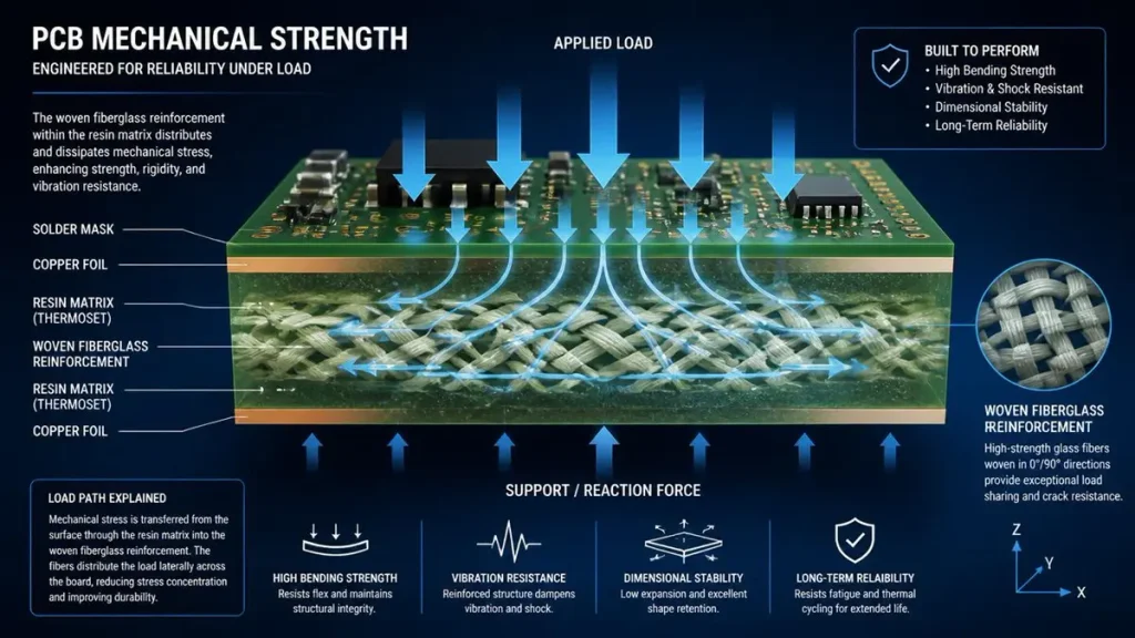
PCB Glass Fibre Mechanical Strength and Load Path Analysis
Direct answer: Glass‑fiber reinforcement increases the mechanical strength and stiffness of a PCB laminate by carrying mechanical loads through the woven reinforcement structure.
The resin matrix provides bonding and electrical insulation, while the glass fibers provide much of the structural reinforcement.
When an external load is applied:
Mechanical force → laminate deformation → glass fibers carry load → reduced deformation
This becomes important for PCBs exposed to:
- Mechanical vibration
- Connector insertion forces
- Heavy components
- Large unsupported areas
- Repeated mounting
- Transportation shock
- Thermal‑mechanical cycling
A large industrial PCB, for example, may be supported only around its perimeter. If the laminate is too flexible, the center section can deflect under component weight or mechanical loading.
That deflection can increase stress around:
- BGA solder joints
- Connectors
- Large components
- Plated through‑holes
- Screw mounting points
Therefore:
Glass reinforcement is not simply a material ingredient; it is part of the PCB’s mechanical load path.
The exact mechanical performance still depends on glass content, resin formulation, laminate thickness, copper distribution, and board geometry.
How Does Flexural Modulus Affect PCB Stiffness?
Direct answer: Flexural modulus indicates how strongly a PCB laminate resists bending deformation, making it an important property when board stiffness and mechanical stability matter.
A higher flexural modulus generally means that greater force is required to produce a given amount of bending.
This matters particularly for:
- Large‑format PCBs
- Backplanes
- Industrial control boards
- Boards with heavy transformers or connectors
- Automotive control modules
- Boards mounted with limited support points
Consider a 400 mm‑class industrial PCB carrying several heavy connectors.
The material itself may satisfy the basic electrical requirements, but excessive mechanical deflection can still create assembly problems.
The engineering chain becomes:
Flexural modulus → board stiffness → deflection → component/solder‑joint stress
For this reason, mechanical material selection should not be separated from the final PCB geometry.
A material property that looks adequate on a small test coupon may not provide the same practical margin on a large board with uneven copper distribution and heavy components.
How Does PCB Glass Fibre Affect CTE?
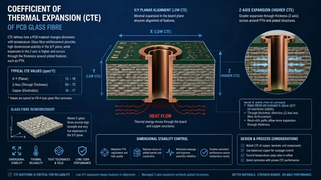
PCB Glass Fibre CTE Thermal Expansion and PTH Reliability Diagram
Direct answer: PCB glass fibre constrains thermal expansion, especially in the X/Y plane, helping improve dimensional stability and reducing thermal‑mechanical movement.
The coefficient of thermal expansion, or CTE, describes how a material changes dimension as temperature changes.
PCB laminates are anisotropic composites, so engineers normally need to consider:
- X‑axis CTE
- Y‑axis CTE
- Z‑axis CTE
X/Y CTE
The woven glass reinforcement constrains the resin matrix in the plane of the board.
Lower and more controlled X/Y expansion helps with:
- Layer registration
- Board dimensions
- Component alignment
- Fine‑pitch structures
- Multilayer dimensional stability
Z‑axis CTE
The Z‑axis is particularly important because plated through‑holes extend through the board thickness.
During heating: PCB expands in Z → copper barrel experiences mechanical strain
During cooling: PCB contracts → copper barrel experiences reverse strain
Repeated thermal cycling can therefore create fatigue stress in the plated copper.
This makes Z‑axis CTE particularly important for thick multilayer PCBs and high‑reliability applications.
Why Is Z‑Axis CTE Important for Plated Through‑Hole Reliability?
Direct answer: Z‑axis CTE matters because excessive thickness‑direction expansion can increase mechanical strain in plated through‑hole copper during repeated temperature changes.
The resin system generally contributes more thermal expansion than the glass reinforcement.
Around and above the resin system’s glass‑transition region, the expansion behavior can change significantly.
A simplified reliability chain is:
Temperature cycling ↓ Z‑axis expansion/contraction ↓ Copper barrel strain ↓ Repeated fatigue ↓ Potential interconnect reliability degradation
This becomes increasingly important when a PCB combines:
- High layer count
- Thick dielectric construction
- Small plated holes
- Lead‑free assembly
- Severe thermal cycling
- Automotive or industrial environments
However, Z‑axis CTE should never be evaluated alone.
PTH reliability also depends on:
- Hole diameter
- Copper plating thickness
- Aspect ratio
- Resin system
- Board thickness
- Thermal‑cycle profile
- Plating quality
The practical engineering question is therefore:
Does the complete PCB construction provide sufficient thermal‑mechanical reliability?
How Does Glass Fibre Affect PCB Dielectric Constant?
Direct answer: Glass fibre contributes to the effective dielectric environment of the laminate, while the final PCB dielectric constant depends on glass content, resin content, glass style, resin formulation, frequency, and measurement method.
One common design mistake is to treat “fiberglass PCB” as having one universal Dk value.
It does not.
The effective dielectric behavior depends on the composite structure:
Glass + resin + glass distribution + frequency + construction
The glass reinforcement and resin matrix can have different dielectric characteristics.
As a result, the dielectric environment around a PCB trace is not necessarily perfectly homogeneous.
This becomes more important as signal speeds increase.
The engineering relationship is:
Glass structure → effective dielectric environment → propagation velocity → impedance/timing behavior
For conventional low‑speed electronics, local dielectric variation may have limited impact.
For high‑speed serial channels, however, engineers may need to consider the glass weave and the exact laminate construction.
How Does Df Affect High‑Speed PCB Performance?
Direct answer: Dissipation factor, or Df, represents dielectric loss and becomes increasingly important when PCB traces carry high‑frequency signals over significant distances.
A higher dielectric loss can increase signal attenuation.
The practical relationship is:
Df → dielectric loss → channel attenuation → reduced signal margin
Df should therefore be evaluated together with:
- Dk
- Frequency
- Trace length
- Copper roughness
- Trace geometry
- Reference‑plane structure
- Material construction
A Df value without a defined frequency and test condition is difficult to use for precise engineering comparisons.
Therefore, procurement teams should request frequency‑specific material data rather than comparing isolated numbers from different datasheets.
How Does Glass Weave Affect High‑Speed Signal Integrity?
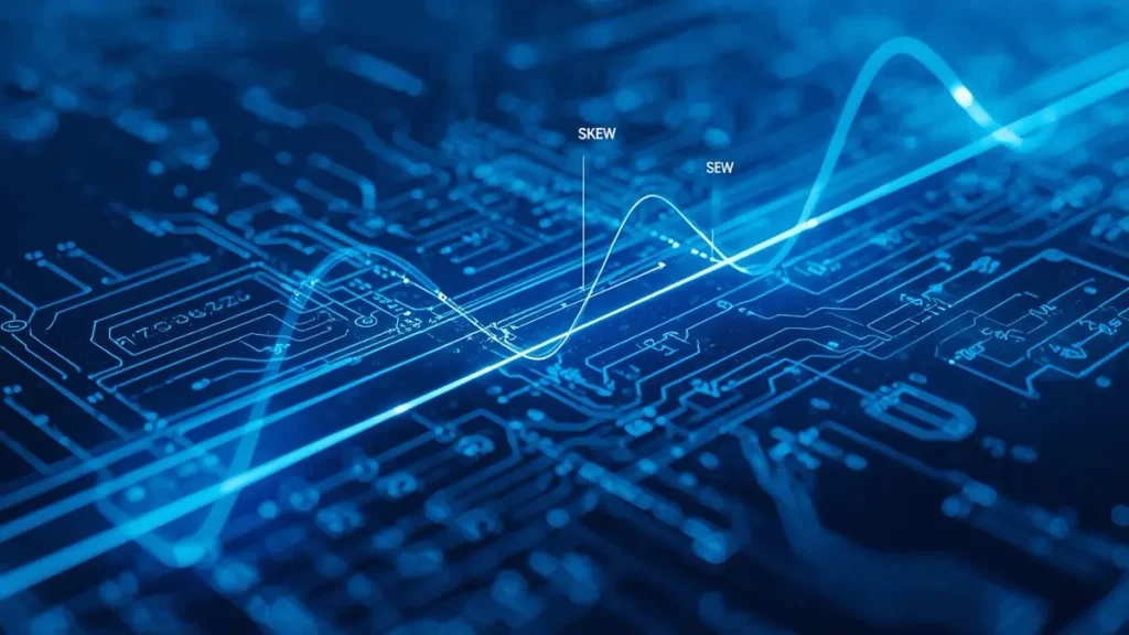
PCB Glass Weave Effect on High-Speed Signal Integrity and Skew
Direct answer: Glass weave can affect high‑speed signal integrity because woven glass creates alternating glass‑rich and resin‑rich regions around a transmission line, producing local dielectric variation.
A conventional glass fabric contains bundles arranged in different directions.
The resulting dielectric structure is therefore not perfectly uniform.
If a differential pair is routed so that its two conductors interact differently with glass‑rich and resin‑rich regions, their propagation characteristics can differ.
Potential consequences include:
- Differential skew
- Local impedance variation
- Timing variation
- Mode conversion
- Channel‑to‑channel variation
The problem becomes more relevant as:
- Data rates increase
- Channel lengths increase
- Rise/fall times become faster
- Timing margins become smaller
- Differential‑pair skew budgets become tighter
How can engineers reduce glass‑weave risk?
Depending on the design, engineers may consider:
- Different glass styles
- Spread‑glass constructions
- Trace positioning
- Differential‑pair routing strategy
- Stack‑up optimization
- Frequency‑specific material characterization
The key point is:
Glass weave is simultaneously a mechanical reinforcement structure and part of the electrical environment surrounding a high‑speed transmission line.
When Does the Glass‑Weave Effect Matter Most?
Direct answer: The glass‑weave effect deserves greater attention in high‑speed, long‑channel, tightly timed differential interfaces than in conventional low‑speed control circuits.
| Design Condition | Glass‑Weave Concern |
|---|---|
| Low‑speed control | Usually low |
| Short digital trace | Usually limited |
| Moderate‑speed digital | Application dependent |
| High‑speed serial | Higher |
| Long differential channel | Higher |
| Tight skew budget | High |
| High data‑rate interconnect | High |
There is no universal frequency at which glass weave suddenly becomes a problem.
The appropriate threshold depends on:
- Signaling technology
- Channel length
- Rise time
- Dielectric thickness
- Trace geometry
- Allowable skew
- System‑level SI margin
This is why glass‑weave evaluation should be driven by the actual channel budget rather than a generic data‑rate rule.
How Does Glass Style Affect PCB Thickness and Dimensional Stability?
Direct answer: Glass style affects the distribution of reinforcement within a dielectric layer and therefore influences pressed thickness, resin content, resin flow, dimensional stability, and dielectric behavior.
Common PCB glass styles include:
- 106
- 1067
- 1080
- 1078
- 2116
- 7628
These are not interchangeable simply because they are all fiberglass.
Different constructions have different:
- Fabric thickness
- Glass density
- Resin capacity
- Reinforcement distribution
- Pressed dielectric behavior
For example, a thin HDI dielectric layer may require a different glass construction from a thick multilayer core.
The correct engineering relationship is:
Glass style → reinforcement distribution → resin content → pressed thickness → electrical/mechanical behavior
Therefore:
Glass style should be selected as part of the complete PCB stack‑up, not as an isolated purchasing item.
How Does Glass‑to‑Resin Ratio Affect PCB Properties?
Direct answer: The glass‑to‑resin ratio changes the balance between mechanical reinforcement and dielectric matrix, influencing stiffness, CTE, effective Dk, resin flow, and final laminate behavior.
A glass‑rich construction generally has a greater reinforcement contribution.
A resin‑rich construction provides more polymer matrix.
These differences can influence:
- Mechanical stiffness
- Dimensional stability
- Dielectric behavior
- Resin flow
- Pressed thickness
- Lamination performance
However, it is incorrect to assume that increasing either glass or resin always improves PCB performance.
The correct material depends on the application.
For example:
Mechanical priority → greater reinforcement may be advantageous
while:
Fine dielectric construction → resin content and glass distribution may require different optimization.
This is why engineers should evaluate the complete laminate construction rather than a single glass‑content percentage.
How Does Glass Fibre Affect PCB Thermal Reliability?
Direct answer: Glass fibre improves thermal‑mechanical stability primarily by constraining dimensional expansion, while the resin system determines important thermal transition characteristics such as Tg.
This distinction is important.
Tg
The glass transition temperature is primarily associated with the polymer resin system.
CTE
Glass reinforcement strongly influences the composite’s dimensional expansion.
Td
Decomposition temperature represents a different thermal property related to material degradation.
Therefore:
Tg ≠ Td ≠ operating temperature
A higher Tg material may provide a useful reliability advantage in some thermal environments, but it should not be interpreted as the maximum allowable PCB operating temperature.
For thermal reliability, engineers should evaluate:
- Tg
- Td
- X/Y CTE
- Z‑axis CTE
- Thermal cycling
- Resin system
- Copper structure
- Board thickness
The finished PCB is the reliability system—not the glass fiber alone.
How Does Moisture Absorption Affect Glass Fiber PCB Reliability?
Direct answer: Moisture behavior depends mainly on the resin system and fiber‑resin interface, but the composite structure influences how moisture interacts with the finished laminate.
Moisture can affect:
- Dielectric behavior
- Insulation resistance
- Thermal processing
- Mechanical properties
- Long‑term reliability
A simplified chain is:
Humidity exposure → moisture uptake → material property change → electrical/mechanical impact
This is particularly relevant for:
- Automotive electronics
- Outdoor electronics
- Industrial control systems
- High‑voltage applications
- Humid operating environments
The actual moisture performance should be verified using the exact material grade and applicable test method.
A generic “fiberglass PCB moisture absorption” number is not sufficient for qualification.
How Does the Glass‑Fiber/Resin Interface Affect Reliability?
Direct answer: The fiber‑resin interface transfers mechanical stress between the glass reinforcement and polymer matrix, making interface quality important for composite strength and reliability.
A PCB laminate works effectively when the reinforcement and resin behave as a mechanically integrated system.
The interface influences:
- Mechanical strength
- Delamination resistance
- Moisture behavior
- Thermal‑cycle performance
- Structural integrity
The engineering chain is:
Glass surface treatment + compatible resin + good bonding ↓ Effective stress transfer ↓ Stable composite structure ↓ Improved reliability
A weak interface can create localized separation under repeated thermal or mechanical loading.
Therefore, high‑reliability material selection should consider the complete laminate system rather than the nominal glass‑fiber specification alone.
How Does Glass Fibre Affect PCB Mechanical Anisotropy?
Direct answer: Woven glass creates directional reinforcement, so mechanical and dimensional behavior can differ between the X and Y directions.
Glass fabric contains warp and fill directions.
As a result, the composite can exhibit direction‑dependent:
- Expansion
- Shrinkage
- Stiffness
- Dimensional movement
This becomes more important for:
- Large PCBs
- Thin PCBs
- High‑layer‑count boards
- Fine‑pitch structures
- Tight registration requirements
Copper distribution also contributes to dimensional behavior.
For example, an asymmetric stack‑up with significantly different copper density between layers can create warpage even when the laminate itself has stable material properties.
Therefore:
Material stability and stack‑up symmetry must be considered together.
Which Glass‑Fiber Properties Matter Most for Different PCB Applications?
Direct answer: The most important glass‑fiber properties depend on the application’s dominant failure mechanisms.
| Application | Priority Properties | Main Engineering Concern |
|---|---|---|
| Consumer electronics | Strength, dimensional stability | Manufacturability |
| Industrial electronics | CTE, stiffness | Thermal/mechanical reliability |
| Automotive | CTE, interface reliability | Thermal cycling |
| High‑layer‑count PCB | CTE, glass style | Registration |
| High‑speed PCB | Glass weave, Dk, Df | Signal integrity |
| HDI PCB | Glass style, resin behavior | Fine dielectric construction |
| Power electronics | CTE, stiffness | Thermal‑mechanical stress |
| Backplane | Flexural modulus, CTE | Deflection |
| High‑voltage PCB | Moisture, insulation properties | Electrical reliability |
The correct selection therefore starts with the application’s failure modes.
How Should Engineers Evaluate Glass Fiber PCB Properties?
Direct answer: Engineers should evaluate each glass‑fiber property against a specific PCB requirement instead of comparing isolated material numbers.
A practical evaluation process is:
Step 1: Define the mechanical requirement
Determine:
- Board dimensions
- Mounting method
- Component weight
- Mechanical support
- Vibration exposure
Then evaluate: Flexural modulus + glass reinforcement + board geometry
Step 2: Define the thermal requirement
Determine:
- Operating temperature
- Assembly temperature
- Thermal cycling
- Expected lifetime
Then evaluate: Tg + CTE + thermal reliability
Step 3: Define the electrical requirement
Determine:
- Signal speed
- Channel length
- Impedance requirement
- Loss budget
Then evaluate: Dk + Df + glass weave + dielectric construction
Step 4: Define the environment
Evaluate:
- Humidity
- Temperature
- Chemical exposure
- Bias conditions
Then evaluate: Moisture behavior + insulation reliability + interface quality
Step 5: Confirm manufacturing compatibility
Finally check:
- Glass style
- Prepreg construction
- Pressed dielectric thickness
- Lamination window
- Registration requirements
- Drilling requirements
This converts material selection from a datasheet comparison into an engineering risk assessment.
What Are the Main Property‑to‑Failure Relationships in a Fiberglass PCB?
Direct answer: The most useful way to evaluate PCB fiberglass material is to connect each property to the failure mechanism it can influence.
| Property | Engineering Effect | Potential Risk |
|---|---|---|
| Flexural modulus | Controls bending resistance | Board deflection |
| X/Y CTE | Controls planar movement | Registration shift |
| Z‑axis CTE | Controls thickness expansion | PTH fatigue |
| Dk | Controls propagation behavior | Impedance/timing variation |
| Df | Controls dielectric loss | Signal attenuation |
| Glass weave | Changes local dielectric environment | Skew/mode conversion |
| Moisture absorption | Changes material behavior | Insulation/reliability risk |
| Fiber/resin adhesion | Transfers mechanical stress | Delamination |
| Glass style | Changes dielectric construction | Thickness variation |
| Glass/resin ratio | Changes composite balance | Mechanical/electrical trade‑off |
This is the engineering model buyers should use when comparing fiberglass PCB materials.
What Should a Glass Fiber PCB Material Specification Include?
Direct answer: A professional specification should identify the exact material construction and define the properties relevant to the PCB’s electrical, mechanical, thermal, and environmental requirements.
Material identification
Specify:
- Laminate manufacturer
- Exact material grade
- Glass style
- Resin system
- Core/prepreg construction
- Copper foil
Mechanical properties
Specify where applicable:
- Flexural modulus
- Tensile strength
- Dimensional stability
- Board stiffness requirement
Thermal properties
Specify:
- Tg
- Td
- X/Y CTE
- Z‑axis CTE
- Thermal‑cycle requirement
Electrical properties
Specify:
- Dk
- Df
- Measurement frequency
- Test method
- Impedance requirement
- Impedance tolerance
Environmental properties
Specify:
- Moisture absorption
- Insulation requirements
- CAF resistance where applicable
- Environmental qualification
The critical procurement rule is:
Always verify material properties against the exact manufacturer’s current datasheet and defined test conditions.
A generic “FR‑4 property” table should not be used as the sole qualification document.
What Is the Difference Between a Material Property and a Finished PCB Property?
Direct answer: A material property describes the behavior of a defined material or laminate under a specified test condition, while finished PCB behavior also depends on stack‑up, copper distribution, geometry, processing, and assembly.
The final board is:
Glass fiber + resin + copper + stack‑up + lamination + geometry + environment
For example, a laminate may have a well‑controlled CTE, but the finished PCB can still experience warpage because of:
- Uneven copper distribution
- Stack‑up asymmetry
- Different dielectric constructions
- Lamination behavior
- Panel constraints
Similarly, a material’s nominal Dk does not automatically equal the effective dielectric environment seen by every high‑speed trace.
This distinction is essential when moving from material qualification to PCB design qualification.
What Are the Key Engineering Lessons About PCB Glass Fibre?
Direct answer: PCB glass fibre should be treated as a structural and electrical component of the laminate system, not simply as a reinforcement material.
The most important engineering relationships are:
Glass reinforcement → mechanical strength Glass reinforcement → flexural modulus → PCB stiffness Glass structure → CTE → dimensional stability Z‑axis CTE → thermal expansion → PTH reliability Glass/resin distribution → effective Dk → signal propagation Df → dielectric loss → high‑speed attenuation Glass weave → local dielectric variation → skew Fiber/resin interface → stress transfer → reliability Glass style + resin content → dielectric construction → stack‑up behavior
These relationships provide a more useful engineering framework than simply asking whether a PCB uses fiberglass.
The right question is:
Which glass‑fiber architecture provides enough engineering margin for the electrical, mechanical, thermal, environmental, and manufacturing requirements of the finished PCB?
PCB Glass Fiber Properties FAQ
What are the properties of PCB glass fibre?
The major properties include mechanical strength, flexural modulus, CTE, dimensional stability, glass style, glass weave, dielectric contribution, moisture behavior, and fiber‑resin interface performance.
What is PCB glass fiber used for?
PCB glass fiber is primarily used as reinforcement in the laminate. It provides mechanical strength and stiffness while helping control dimensional movement and thermal expansion.
Does glass fiber affect PCB signal integrity?
Yes. The glass weave creates local differences in the dielectric environment around traces. This can become relevant in high‑speed differential channels where skew and impedance margins are tightly controlled.
How does glass weave affect high‑speed PCB design?
Glass weave can cause local dielectric variation when signal traces interact differently with glass bundles and resin‑rich regions. For demanding high‑speed links, engineers may need to consider glass style, trace placement, spread‑glass options, and stack‑up construction.
How do I choose glass fiber PCB material?
Start with the application’s mechanical, thermal, electrical, environmental, and manufacturing requirements. Then compare the exact laminate grade, glass style, CTE, Tg, Dk, Df, moisture behavior, and dimensional stability against the PCB’s design requirements.
Ask Our PCB Engineers About Material Selection
Selecting PCB fiberglass material should begin with the engineering requirements of the finished board—not simply with a generic “FR‑4” or “glass fiber” label.
Our engineers can help review requirements involving:
- High‑layer‑count multilayer PCBs
- Tight dimensional stability
- Thermal cycling
- High‑speed signaling
- Controlled impedance
- Fine‑line PCB construction
- HDI structures
- Automotive electronics
- Industrial electronics
- High‑reliability applications
For a material review, provide the available: Layer count + finished thickness + board size + copper thickness + operating temperature + signal speed + impedance requirements + reliability requirements
The goal is to match the glass‑fiber property profile to the actual engineering risk before production.
Ask Our PCB Engineers About Material Selection.
About Author
David Chen https://www.linkedin.com/in/pcbcoming
David Chen boasts an extensive professional background in PCBA manufacturing, PCBA testing, and PCBA optimization, with specialized expertise in high-precision PCBA fault analysis and rigorous PCBA reliability testing. The author has worked with high-layer-count server PCB fabrication, ultra-low-loss backplane stackups, and thermo-mechanical reliability optimization for AI infrastructure projects involving 112G and 224G PAM4 architectures. Skilled in complex circuit design and cutting-edge advanced PCB manufacturing processes, he delivers solutions that elevate product durability and performance across industrial applications. His technical articles focusing on PCBA manufacturing workflows and testing methodologies are widely cited by industry peers, research institutions, and technical platforms, solidifying his reputation as a recognized technical authority in the global circuit board manufacturing sector.