Glass Epoxy PCB: E-Glass, Resin, Properties & Material Selection
Glass epoxy PCB uses woven glass fiber reinforcement combined with an epoxy resin system and copper foil to create a mechanically stable, electrically insulating circuit‑board laminate. The actual performance of a glass epoxy PCB depends not only on whether it is classified as FR‑4, but also on glass style, resin content, Tg, CTE, Dk, Df, copper construction, lamination conditions, and the selected laminate grade.
For engineers and procurement teams, this distinction matters. Two boards may both be described as “FR‑4 glass epoxy PCB” while behaving differently during lamination, thermal cycling, impedance control, drilling, plating, and high‑speed signal transmission.
This guide explains how the glass‑epoxy material system affects PCB design and manufacturing—and how to specify the right material before production.
What Is a Glass Epoxy PCB?
A glass epoxy PCB is a printed circuit board manufactured from copper‑clad laminate or prepreg systems in which woven glass fiber provides mechanical reinforcement and epoxy resin provides dielectric insulation and bonding.
A typical glass epoxy PCB contains:
- Copper foil
- Glass‑fiber reinforcement
- Epoxy resin
- Core laminate
- Prepreg
- Conductive circuit patterns
- Plated through‑holes or microvias in advanced constructions
The glass fabric provides structural reinforcement, while the resin fills the spaces between glass bundles and bonds the laminate structure together.
This combination provides a useful balance of:
- Mechanical strength
- Electrical insulation
- Dimensional stability
- Thermal resistance
- Manufacturability
- Cost
That is why glass epoxy materials remain widely used for multilayer PCBs, industrial electronics, automotive electronics, networking equipment, consumer electronics, and many other applications.
However, “glass epoxy” should not be treated as a single universal material. The actual laminate grade can significantly change the board’s electrical, thermal, mechanical, and manufacturing behavior.
How Is Glass Epoxy PCB Material Constructed?
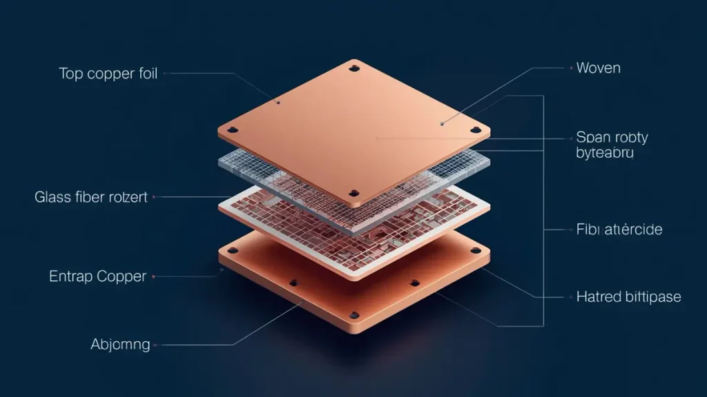
Glass Epoxy PCB Layer Stack-up Exploded Structure
Glass epoxy laminate is built from woven glass reinforcement impregnated with an epoxy resin system and bonded to copper foil. In multilayer PCBs, different core and prepreg constructions are combined to achieve the required finished thickness and electrical performance.
A simplified cross‑section looks like this: Copper Foil → Glass/Epoxy Dielectric → Copper Foil
For a multilayer board, the structure becomes more complex: Copper / Core / Prepreg / Inner Copper / Prepreg / Core / Prepreg / Copper
The final dielectric thickness is affected by several variables:
| Material or Process Variable | Main Effect |
|---|---|
| Glass style | Reinforcement and resin distribution |
| Resin content | Dielectric composition and flow |
| Prepreg thickness | Final dielectric thickness |
| Copper pattern density | Resin‑flow behavior |
| Lamination temperature | Resin softening and curing |
| Lamination pressure | Consolidation and thickness |
| Vacuum condition | Void control |
| Cure profile | Resin cross‑linking and Tg development |
One important engineering principle is: The laminate datasheet does not automatically equal the final dielectric structure inside the finished PCB.
The finished dielectric is the result of material selection + glass style + resin content + copper geometry + stack‑up + lamination process.
Why Does E‑Glass Reinforcement Matter in a Glass Epoxy PCB?
E‑glass reinforcement provides the mechanical framework of the laminate and strongly influences dimensional stability, thermal expansion, stiffness, dielectric behavior, and drilling characteristics.
E‑glass is widely used because it combines:
- High tensile strength
- Good electrical insulation
- Thermal stability
- Chemical resistance
- Relatively low cost
- Established PCB processing compatibility
The glass fibers are organized into woven fabrics. Instead of thinking of the laminate as a uniform block of resin, engineers should think of it as a composite material containing: Glass bundles + resin‑rich areas + copper interfaces
This structure creates local differences in dielectric composition. That becomes especially important for high‑speed signals. A high‑speed trace crossing directly over a dense glass bundle does not necessarily experience exactly the same dielectric environment as a trace passing through a resin‑rich region. Therefore, glass reinforcement is not merely a mechanical component. It can also influence signal integrity.
How Does Glass Style Change Glass Epoxy PCB Properties?
Glass style controls the distribution and volume of glass reinforcement and resin, affecting dielectric thickness, mechanical stiffness, resin flow, dimensional stability, and high‑speed signal behavior.
Different glass styles can produce different laminate constructions even when the nominal resin system is similar. The engineering relationship can be simplified as: Glass Style → Glass/Resin Distribution → Effective Dielectric Behavior → PCB Performance
Important variables include:
- Glass fabric thickness
- Yarn density
- Weave geometry
- Glass/resin ratio
- Fabric orientation
- Number of plies
- Prepreg construction
Why does this matter during PCB manufacturing?
Consider two multilayer designs with identical nominal dielectric thickness. If one construction uses a different glass style or resin content, its behavior during pressing may differ. The consequences can include:
- Different resin flow
- Different final dielectric thickness
- Different local Dk
- Different impedance
- Different dimensional movement
- Different copper‑to‑copper registration behavior
This is one reason why engineers should not select prepreg only by its nominal thickness. The pressed thickness under the actual copper pattern matters.
How Does Epoxy Resin Affect Glass Epoxy PCB Performance?
The epoxy resin system determines much of the laminate’s thermal, electrical, chemical, and bonding performance, including Tg, moisture behavior, resin flow, curing characteristics, and dielectric loss.
A PCB resin system can be engineered for different performance requirements. Typical design objectives include:
- Higher thermal resistance
- Lower dielectric loss
- Better dimensional stability
- Improved chemical resistance
- Better moisture resistance
- Higher thermal reliability
- Controlled resin flow
- Lead‑free assembly compatibility
The resin system also determines how the material behaves during lamination. During pressing, the resin transitions from a relatively solid prepreg state into a softened, flowing state and eventually into a cured polymer network. The process must control: Heat → Resin Flow → Wetting → Consolidation → Cure
If the process window is poorly controlled, the board can experience:
- Voids
- Resin starvation
- Excessive resin squeeze‑out
- Uneven dielectric thickness
- Poor bonding
- Registration problems
- Local delamination
This is why material selection and lamination engineering cannot be completely separated.
How Does Resin Content Affect Glass Epoxy PCB Thickness and Impedance?
Resin content influences the amount of polymer available to fill the spaces around glass reinforcement and copper structures, affecting pressed dielectric thickness, resin flow, effective dielectric properties, and impedance control.
A simplified relationship is: Higher resin content → more resin available for flow and filling while: Higher glass content → greater reinforcement contribution and lower available resin volume
However, this should not be interpreted as a simple “higher is better” relationship. The required resin content depends on:
- Copper pattern density
- Adjacent copper planes
- Prepreg construction
- Target dielectric thickness
- Lamination pressure
- Temperature profile
- Final impedance requirement
Example: Dense multilayer power plane
A prepreg construction that works well between relatively uniform copper planes may behave differently when one layer contains heavy copper areas and another contains sparse routing. During lamination, resin may flow from high‑resin areas toward lower‑resistance flow paths. This can create local dielectric‑thickness variation.
For controlled impedance, the engineer therefore needs to evaluate: Trace Width + Copper Thickness + Dielectric Thickness + Effective Dk + Reference Plane Geometry rather than relying on trace width alone.
How Do Tg and CTE Affect Glass Epoxy PCB Reliability?
Tg indicates a major transition in polymer behavior, while CTE describes dimensional expansion. Together with the copper structure and plated‑hole geometry, they influence thermal reliability.
Glass Epoxy PCB Tg
The glass transition temperature, or Tg, is associated with a significant change in the mechanical behavior of the cured resin system. For PCB applications, Tg should be evaluated together with:
- Operating temperature
- Assembly temperature
- Lead‑free reflow exposure
- Thermal cycling
- Board thickness
- Copper distribution
- Plated‑hole structure
A higher Tg can provide greater thermal margin, but higher Tg alone does not guarantee better reliability.
Z‑Axis CTE
The Z‑axis is particularly important because multilayer PCBs contain plated through‑holes extending through the board thickness. During thermal cycling: PCB expands → PCB contracts → copper barrel experiences mechanical strain
Repeated strain can contribute to:
- Barrel cracking
- Corner cracking
- Plated‑hole reliability problems
- Interconnect fatigue
For high‑reliability boards, engineers should therefore evaluate Tg and Z‑axis CTE together rather than using Tg as the only material‑selection criterion.
How Should Engineers Compare Standard and High‑Tg Glass Epoxy PCB Materials?
Standard glass epoxy is appropriate for many general‑purpose designs, while high‑Tg materials become more attractive when thermal exposure, repeated thermal cycling, lead‑free assembly, or long‑term reliability creates additional material demands.
A practical comparison is:
| Requirement | Standard Glass Epoxy | High‑Tg Glass Epoxy |
|---|---|---|
| General electronics | Usually suitable | May be unnecessary |
| Cost‑sensitive design | Strong option | Higher material cost may apply |
| High assembly temperature | Application‑dependent | More thermal margin |
| Thermal cycling | Application‑dependent | Often preferred |
| Automotive electronics | Depends on qualification | Frequently evaluated |
| Industrial controls | Common | Useful for harsher environments |
| High layer count | Possible | Depends on stack‑up |
| High‑speed signals | Possible | Dk/Df must still be checked |
The correct question is not:
“Is high‑Tg always better?”
The better question is:
“What thermal and reliability requirements does this PCB actually have?”
For many applications, upgrading material without a corresponding reliability requirement simply increases material cost.
How Does Glass Epoxy PCB Material Affect High‑Speed Signal Integrity?
Glass epoxy material affects high‑speed performance through dielectric constant, dissipation factor, resin/glass distribution, glass weave, dielectric thickness, and conductor‑loss behavior.
For high‑speed designs, the important parameters include:
Dielectric Constant — Dk
Dk influences the electromagnetic propagation characteristics of the transmission line and therefore affects impedance and signal delay. However, Dk is not always one universal number. It can vary with:
- Frequency
- Resin content
- Glass content
- Measurement method
- Material formulation
- Direction
Dissipation Factor — Df
Df represents dielectric loss behavior. As signaling frequency increases, dielectric loss becomes increasingly important in the total channel‑loss budget. Therefore, a high‑speed PCB material should be evaluated using the manufacturer’s frequency‑specific data whenever available.
Glass Weave
Glass weave can create local variations in the dielectric environment. For differential pairs, this may contribute to:
- Intra‑pair skew
- Local impedance variation
- Mode conversion
- Timing differences
For demanding high‑speed channels, engineers may therefore consider:
- Fine‑weave glass
- Spread‑glass structures
- Trace routing strategy
- Pair positioning
- Stack‑up symmetry
Why Is Glass Weave Important for High‑Speed PCB Signal Integrity?
Glass weave matters because the electromagnetic field around a high‑speed trace interacts with regions containing different proportions of glass and resin, creating local dielectric variation.
Imagine a differential pair running across a woven glass structure. If one conductor primarily sees a glass‑rich region while the other encounters a resin‑rich region, the two conductors can experience slightly different propagation conditions. The resulting problem is not necessarily a dramatic impedance failure. It can instead appear as a smaller but important timing or skew issue.
This becomes increasingly relevant as data rates rise. For conventional low‑speed digital signals, this effect may be negligible. For high‑speed channels, engineers should consider the complete structure: Material → Glass Weave → Stack‑Up → Trace Geometry → Connector → Via → Package
The material decision therefore becomes part of the overall signal‑integrity design.
How Does Copper Roughness Interact With Glass Epoxy PCB Performance?
Copper surface roughness can increase conductor loss at high frequencies because current increasingly concentrates near the conductor surface as frequency rises.
For conventional PCB applications, copper roughness may have limited impact. For high‑speed and high‑frequency channels, however, conductor loss can become a meaningful part of the insertion‑loss budget.
Engineers may therefore evaluate:
- Copper foil type
- Surface roughness
- Trace geometry
- Frequency
- Dk
- Df
- Total transmission‑line length
This is especially important when a glass epoxy system is being considered for high‑speed networking or data‑center electronics. Material selection should therefore consider both: Dielectric Loss + Conductor Loss rather than Df alone.
What Happens to Glass Epoxy PCB During Lamination?
During lamination, heat and pressure cause the resin to soften, flow, fill the required spaces, and cure into a rigid dielectric structure. The process determines the final thickness, bonding quality, registration and internal reliability.
A simplified process sequence is: Prepreg Preparation ↓ Stack‑Up Assembly ↓ Vacuum / Lamination ↓ Resin Softening ↓ Controlled Resin Flow ↓ Cure ↓ Cooling ↓ Finished Multilayer Structure
The difficult part is controlling the process window. Too little resin flow can contribute to:
- Resin starvation
- Voids
- Incomplete filling
Excessive resin flow can contribute to:
- Dielectric‑thickness variation
- Resin squeeze‑out
- Local dimensional changes
Uneven copper distribution can make the situation more difficult.
Practical manufacturing scenario
Suppose one region of a multilayer PCB contains a large copper plane while another region contains sparse signal traces. The two regions can present different resin‑flow conditions during pressing. The result may be a local difference in:
- Dielectric thickness
- Resin distribution
- Surface flatness
- Dimensional movement
This is why advanced multilayer PCB manufacturing requires stack‑up engineering rather than simply stacking commercially available prepreg sheets.
What Manufacturing Problems Are Related to Glass Epoxy Material Behavior?
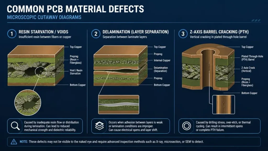
Common Glass Epoxy PCB Material Defects & Causes
The most important material‑related manufacturing problems include resin starvation, excessive resin flow, dielectric‑thickness variation, warpage, delamination, drilling stress, and plated‑hole reliability issues.
| Material / Process Issue | Manufacturing Effect | Potential Result |
|---|---|---|
| Insufficient resin flow | Incomplete filling | Voids or resin starvation |
| Excessive resin flow | Thickness variation | Impedance deviation |
| High Z‑axis expansion | PTH stress | Barrel cracking |
| Poor curing | Weak resin network | Reliability degradation |
| Moisture uptake | Vapor generation during heat | Delamination risk |
| Uneven glass/resin distribution | Local Dk variation | SI variation |
| Uneven copper distribution | Asymmetric lamination | Warpage |
| Incorrect material pairing | CTE mismatch | Registration/reliability issues |
These problems are not solved by choosing a laminate with a higher price. They require alignment between: Material → Stack‑Up → Lamination → Drilling → Plating → Inspection
How Do LDI, Laser Drilling and mSAP Improve Glass Epoxy PCB Manufacturing?
Modern PCB manufacturing technologies improve dimensional accuracy, fine‑feature formation, interconnect density, and process control while allowing glass epoxy materials to support increasingly complex multilayer structures.
LDI — Laser Direct Imaging
LDI improves image‑registration control by directly exposing the circuit pattern without relying on conventional photographic tooling. For fine‑line glass epoxy multilayer boards, this can help manage:
- Fine trace geometry
- Registration
- Layer‑to‑layer alignment
Laser Drilling
Laser drilling is widely used for microvia structures. For HDI glass epoxy boards, laser drilling allows smaller interconnect structures than conventional mechanical drilling. Process control remains important because glass reinforcement can influence drilling behavior and hole‑wall quality.
mSAP
Modified Semi‑Additive Processing can support fine‑line circuit formation by controlling copper deposition and pattern formation more precisely. This is particularly useful when conventional subtractive etching becomes difficult to apply to very fine circuit geometries.
Controlled Lamination
For high‑layer‑count glass epoxy PCBs, controlled lamination remains fundamental. Modern production should monitor:
- Temperature profile
- Pressure
- Vacuum
- Resin‑flow behavior
- Cure
- Registration
- Final thickness
AOI and X‑Ray Inspection
AOI can detect surface and circuit‑pattern defects. X‑ray inspection can be used where internal structures require non‑destructive evaluation. For critical multilayer boards, microsection analysis can provide direct evidence of:
- Plated‑hole quality
- Copper thickness
- Dielectric thickness
- Via structures
- Internal bonding
What Material Specification Should Buyers Include in a Glass Epoxy PCB RFQ?
A professional glass epoxy PCB RFQ should specify the laminate family, required thermal properties, electrical requirements, construction, reliability requirements, and applicable material qualification—not simply state “FR‑4.”
A useful material section should include:
Material Identification
- Manufacturer
- Laminate family
- Specific grade
- Core material
- Prepreg family
- Copper foil type
Thermal Requirements
- Tg requirement
- Td where applicable
- Z‑axis CTE
- Thermal cycling requirement
- Reflow exposure
Electrical Requirements
- Dk
- Df
- Frequency of interest
- Controlled impedance
- Impedance tolerance
Mechanical Requirements
- Board thickness
- Dimensional tolerance
- Warpage requirement
- Peel‑strength requirement
Reliability Requirements
- Plated‑hole reliability
- Thermal cycling
- Moisture resistance
- CAF requirements where applicable
- Applicable automotive/industrial requirements
Manufacturing Information
- Layer count
- Copper thickness
- Minimum trace/space
- Via structure
- HDI requirements
- Surface finish
The more demanding the PCB, the less useful the generic specification:
“FR‑4 material”
becomes. A specific laminate grade and construction should be agreed before production whenever material properties materially affect performance.
Which Glass Epoxy PCB Material Should Be Used for Different Applications?
Material selection should follow the electrical, thermal, mechanical, reliability, and manufacturing requirements of the application rather than simply choosing the highest‑performance laminate.
| Application | Typical Material Direction | Key Selection Criteria |
|---|---|---|
| Consumer electronics | Standard glass epoxy | Cost, manufacturability |
| Industrial control | Standard / high‑Tg | Temperature, reliability |
| Automotive electronics | High‑Tg or qualified FR‑4 family | Thermal cycling, reliability |
| High‑layer‑count board | Controlled glass/epoxy construction | Registration, CTE |
| High‑speed networking | Low‑loss glass/epoxy or advanced laminate | Dk, Df, weave |
| AI/data‑center hardware | High‑speed material system | Loss, impedance, thermal behavior |
| Power electronics | Thermal/reliability‑focused material | CTE, heat, copper structure |
| HDI electronics | Compatible glass/epoxy laminate | Laser drilling, dimensional stability |
This table should be treated as an engineering starting point rather than a universal material prescription. The final choice should be based on the actual design requirements and the selected material manufacturer’s datasheet.
When Should Engineers Move Beyond Standard FR‑4 Glass Epoxy PCB?
Engineers should consider moving beyond standard FR‑4 when thermal reliability, signal loss, dielectric stability, dimensional control, or application‑specific qualification requirements exceed the practical margin of the selected standard material.
A material upgrade becomes worth evaluating when:
- Signal frequency increases
- Channel loss becomes difficult to control
- Differential‑pair skew becomes important
- Thermal cycling becomes severe
- Operating temperature increases
- Layer count increases significantly
- Impedance tolerance becomes tighter
- PTH reliability becomes critical
- Automotive or industrial qualification becomes mandatory
The decision should follow: Requirement → Failure Risk → Material Property → Manufacturing Capability not: Expensive Material → Better PCB
This approach usually produces a more defensible engineering decision and can avoid unnecessary material costs.
How Does Glass Epoxy Material Selection Affect PCB Cost?
The laminate grade is only one part of PCB cost, but material selection can influence material price, lamination complexity, manufacturing yield, processing time, and qualification requirements.
A lower‑cost material may not actually be cheaper if it causes:
- More difficult impedance control
- Higher scrap
- More rework
- More thermal‑cycle failures
- More complex lamination
- Additional qualification cycles
Conversely, an unnecessarily expensive low‑loss or high‑Tg material can increase cost without providing a measurable product benefit.
The practical target is therefore:
The lowest‑cost material that reliably satisfies the electrical, thermal, mechanical and manufacturing requirements.
How Can Hongda Help With Glass Epoxy PCB Material Selection?
Shenzhen Hongda Circuit Technology Co., Ltd. approaches glass epoxy PCB production from both the material and manufacturing sides, allowing laminate selection to be evaluated together with stack‑up, HDI structures, lamination, fine‑line processing, inspection and production requirements.
Hongda’s published PCB technology portfolio includes multilayer PCB, HDI, high‑frequency/high‑speed PCB, rigid‑flex, heavy‑copper and other advanced PCB manufacturing technologies, with processes including LDI, laser drilling, sequential lamination and mSAP.
For a glass epoxy PCB project, the practical engineering review can focus on:
- Laminate family and grade
- Glass style
- Prepreg construction
- Resin content
- Finished dielectric thickness
- Stack‑up
- Impedance requirements
- Tg and CTE requirements
- Copper distribution
- Via structure
- Lamination feasibility
- Manufacturing tolerance
- Inspection requirements
The objective is not simply to quote a board. It is to ensure that the specified material, stack‑up and manufacturing process are compatible before mass production.
What Should Buyers Check Before Ordering a Glass Epoxy PCB?
Buyers should verify the exact laminate grade, material datasheet, stack‑up, electrical requirements, thermal requirements, manufacturing tolerances, inspection plan and material traceability before releasing production.
A practical procurement sequence is: 1. Define application requirements ↓ 2. Select material family ↓ 3. Confirm laminate grade ↓ 4. Review stack‑up ↓ 5. Verify Dk/Df and impedance ↓ 6. Review Tg/CTE and reliability ↓ 7. Complete DFM review ↓ 8. Approve first article ↓ 9. Validate reliability ↓ 10. Release mass production
This workflow reduces the risk of selecting a material based only on a marketing description such as “high‑Tg FR‑4.”
Glass Epoxy PCB Procurement FAQ
Is FR‑4 the same as glass epoxy PCB?
Not exactly. FR‑4 refers to a flame‑retardant material classification/family, while glass epoxy describes the composite structure using glass reinforcement and epoxy resin. Different FR‑4 laminate grades can have substantially different Tg, Dk, Df, CTE, moisture and processing characteristics.
What Tg should a glass epoxy PCB have?
There is no universal Tg requirement. Standard applications may use conventional FR‑4 grades, while higher‑temperature or thermally cycled applications may justify high‑Tg materials. The correct value should be selected according to assembly temperature, operating temperature, thermal cycling and reliability requirements.
Does glass weave affect high‑speed PCB performance?
Yes. At higher data rates, differences between glass‑rich and resin‑rich regions can affect the local dielectric environment. For demanding differential signaling, engineers may need to consider glass style, spread glass, trace positioning, stack‑up and overall channel design.
Can glass epoxy PCB be used for HDI?
Yes. Glass epoxy laminates are widely used in HDI PCB constructions. The selected material must be compatible with the required laser drilling, microvia formation, sequential lamination, copper plating and dimensional‑control requirements.
How do I choose a glass epoxy PCB manufacturer?
Evaluate more than price. Ask the manufacturer to confirm the exact laminate grade, material traceability, stack‑up capability, lamination control, registration capability, microvia processing, impedance control, inspection methods and experience with your required board thickness, layer count and reliability conditions.
Engineering Takeaway: Glass Epoxy Is a System, Not Just a Material
A glass epoxy PCB should not be specified simply as:
“FR‑4, 1.6 mm.”
For a demanding design, the actual engineering system is: E‑Glass + Epoxy Resin + Glass Style + Resin Content + Copper Foil + Stack‑Up + Lamination Process + Electrical Requirements + Reliability Requirements
The most important engineering lesson is that material properties become meaningful only when connected to the actual PCB structure and manufacturing process.
Tg affects thermal margin. CTE affects dimensional and interconnect reliability. Dk and Df affect signal behavior. Glass weave affects local dielectric uniformity. Resin content affects dielectric construction and lamination behavior. Copper distribution affects resin flow and dimensional stability. And the selected manufacturing process determines whether those material properties can be translated into a consistent production result.
For engineers, the right question is therefore not simply:
“Which glass epoxy PCB material is the best?”
It is:
“Which glass‑epoxy material system provides the required electrical, thermal, mechanical and manufacturing margin for this specific PCB?”
That is the basis for a reliable material‑selection decision.
Request a Glass Epoxy PCB Engineering Review
If you already have a Gerber package, stack‑up, impedance requirement or preliminary material specification, Shenzhen Hongda Circuit Technology Co., Ltd. can review the construction from a manufacturing perspective.
Recommended information to provide:
- Gerber files
- Stack‑up
- Layer count
- Finished thickness
- Copper thickness
- Material requirement
- Tg requirement
- Dk/Df requirement
- Controlled impedance
- HDI/microvia requirements
- Annual or project volume
Need help selecting the laminate before ordering? Request a Glass Epoxy PCB Material Review
Ready for production? Request a Glass Epoxy PCB Quote. Email:pcb@pcbkr.com
About Author
David Chen https://www.linkedin.com/in/pcbcoming
David Chen boasts an extensive professional background in PCBA manufacturing, PCBA testing, and PCBA optimization, with specialized expertise in high-precision PCBA fault analysis and rigorous PCBA reliability testing. The author has worked with high-layer-count server PCB fabrication, ultra-low-loss backplane stackups, and thermo-mechanical reliability optimization for AI infrastructure projects involving 112G and 224G PAM4 architectures. Skilled in complex circuit design and cutting-edge advanced PCB manufacturing processes, he delivers solutions that elevate product durability and performance across industrial applications. His technical articles focusing on PCBA manufacturing workflows and testing methodologies are widely cited by industry peers, research institutions, and technical platforms, solidifying his reputation as a recognized technical authority in the global circuit board manufacturing sector.