Gold Finger PCB Design Guide: Complete Technical Reference for Dimensions, Chamfer, Plating & DFM
By Shenzhen Hongda Circuit Technology Co., Ltd. | Engineering Team
Last Updated: July 2026 | Technical Depth: Advanced | Target Audience: PCB Designers, Hardware Engineers, Procurement Technical Reviewers
Introduction: Why Gold Finger Design Decisions Determine Product Reliability
A gold finger PCB design that looks correct on a schematic can fail catastrophically in the field if chamfer angles, plating tie-bars, solder mask clearances, or inner-layer copper pull-backs are improperly specified. At Shenzhen Hongda Circuit Technology Co., Ltd., our engineering team reviews over 300 gold finger designs monthly, and approximately 35% require DFM corrections before release to production. The most common issues—insufficient solder mask clearance, missing inner-layer copper removal, and incorrect tie-bar routing—are entirely preventable with proper design discipline.
This guide consolidates every critical design parameter for PCB gold finger edge connectors into a single technical reference. Whether you are designing a PCIe 5.0 accelerator card, an industrial PLC backplane, or a medical imaging module, the specifications, tolerances, and DFM rules in this document will ensure your design translates into a manufacturable, reliable product.
IPC Design Standards & Industry Specifications for Gold Finger PCBs
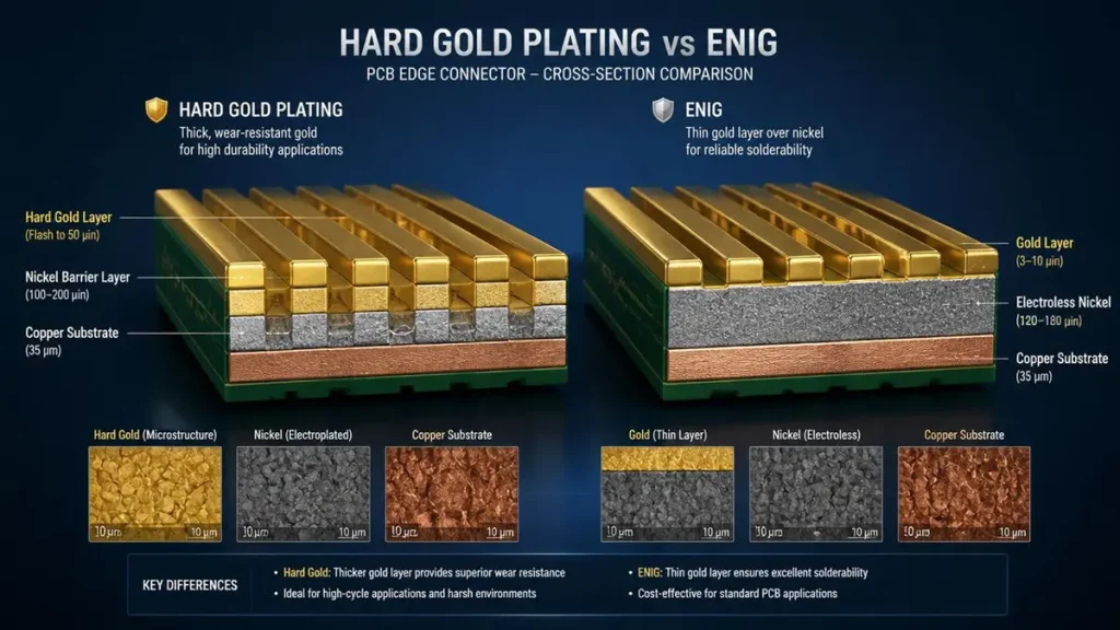
Hard Gold Plating vs. ENIG Cross-Section Comparison for PCB Gold Fingers
Gold finger PCB designs must comply with IPC-2221 (generic PCB design standards), IPC-2226 (HDI design), IPC-6012 (performance and qualification), IPC-A-600 (acceptability), and IPC-4552 (electroplated gold for edge connectors). For high-speed applications, PCI-SIG specifications (PCIe CEM) and JEDEC standards (DDR5 DIMM, M.2) define finger geometry, pitch, and impedance requirements. Military applications add MIL-PRF-31032 and MIL-G-45204 for gold plating composition and thickness.
IPC Standard Hierarchy for Gold Finger Design
| Standard | Design Relevance | Key Gold Finger Requirements |
|---|---|---|
| IPC-2221 | Generic PCB design | Trace width/spacing, annular ring, edge clearance |
| IPC-2222 | Rigid PCB section | Layer stackup, copper weight, dielectric requirements |
| IPC-2226 | HDI/microvia design | Via-in-pad, stacked vias near finger area |
| IPC-6012 Class 2/3 | Performance qualification | Gold thickness, nickel underplate, adhesion, wear testing |
| IPC-A-600 | Visual acceptability | Plating nodules, edge roughness, chamfer defects |
| IPC-4552 | Electroplated gold spec | Gold composition (cobalt 0.2–0.5%), thickness, hardness, porosity |
| IPC-TM-650 2.4.18 | Adhesion testing | Tape test methodology for gold-to-nickel adhesion |
| IPC-TM-650 2.4.24 | Porosity testing | Nitric acid vapor test for gold porosity |
| IPC-TM-650 2.4.42 | Thickness testing | XRF or beta backscatter measurement methods |
| IPC-1752A | Material declaration | RoHS/REACH compliance, conflict minerals |
Hard Gold vs. ENIG: Design Specification Impact
The choice between hard gold (electroplated) and ENIG (immersion) is not merely a material selection—it fundamentally changes the design rules:
| Design Parameter | Hard Gold (Electroplated) | ENIG (Immersion) |
|---|---|---|
| Plating Area Definition | Must define selective plating zone with photoresist mask | Entire pad surface plated automatically |
| Tie-Bar Requirement | Required for current distribution; must be removed post-plating | Not applicable |
| Edge Clearance | 0.5 mm minimum from board edge to finger start | Standard pad clearance rules apply |
| Solder Mask Opening | Must expose entire finger + 0.5 mm beyond | Standard mask expansion (2–4 mils) |
| Chamfer Design | Mandatory; angle specified in fab notes | Not applicable (no edge contact) |
| Inner Layer Copper | Must remove copper under bevel zone (0.6–3.0 mm) | Standard copper pour rules |
| Via Restriction | No vias within 1.0 mm of finger pads | Standard via placement |
| IPC Standard | IPC-4552 (electroplated gold) | IPC-4556 (ENIG) |
Critical Design Rule: If your design includes edge connector contacts that will experience mechanical insertion/removal, you must specify electroplated hard gold per IPC-4552. ENIG is never acceptable for gold finger applications—it will fail within 1–10 insertion cycles.
Gold Thickness Design Selection by Application
| Insertion Cycles | Gold Thickness (μin) | Gold Thickness (μm) | Application Example | IPC-4552 Tier |
|---|---|---|---|---|
| 1–10 | 5–10 | 0.13–0.25 | Prototype, non-functional demo | Type I (minimum) |
| 10–100 | 10–30 | 0.25–0.76 | Consumer gaming cards, low-cycle peripherals | Type I |
| 100–500 | 30–50 | 0.76–1.27 | Standard networking, AI server PCIe | Type II |
| 500–2,000 | 50–100 | 1.27–2.54 | Industrial I/O, automotive diagnostic | Type II |
| 2,000–5,000 | 100–200 | 2.54–5.08 | Telecom backplanes, military avionics | Type III |
| 5,000+ | 200–300 | 5.08–7.62 | Aerospace, extreme-environment test fixtures | Type III |
At Hongda Circuit, our default recommendation for general industrial applications is 30 μ” (0.76 μm) hard gold over 200 μ” (5.08 μm) electrolytic nickel. This combination achieves 1,000+ insertion cycles at <20 mΩ contact resistance, with cost efficiency optimized for medium-volume production.
Gold Finger Dimensions, Pitch & Geometric Parameters
Standard PCB gold finger dimensions include finger width of 1.0–1.5 mm, finger length of 15–30 mm (maximum 40 mm per IPC-4552), pitch (center-to-center spacing) of 1.0–2.54 mm for standard connectors and 0.5–1.0 mm for high-density (PCIe, DDR, M.2). Tolerances: width ±0.05 mm (±2 mils), pitch ±0.05 mm (standard) or ±0.025 mm (high-density), length per connector datasheet. All fingers in a row must maintain consistent length unless implementing intentional long-short (staggered) power sequencing.
Finger Width, Length & Pitch Specification
| Parameter | Standard Range | High-Density Range | Tolerance | Design Notes |
|---|---|---|---|---|
| Finger Width | 1.0–1.5 mm | 0.6–1.0 mm | ±0.05 mm | Wider fingers carry more current; narrower enables higher density |
| Finger Length | 15–30 mm | 10–20 mm | Per connector spec | Max 40 mm to prevent plating uniformity issues |
| Pitch (Standard) | 1.27 mm, 2.0 mm, 2.54 mm | — | ±0.05 mm | Match connector datasheet exactly |
| Pitch (High-Density) | 0.5 mm, 0.635 mm, 0.8 mm, 1.0 mm | — | ±0.025 mm | PCIe x16: 1.0 mm; M.2: 0.5 mm |
| Finger-to-Edge Distance | 0.5–1.0 mm | 0.25–0.5 mm | ±0.05 mm | Prevents beveling into finger copper |
| End-to-End Tolerance | — | — | ±0.1 mm | All fingers in row must be parallel within ±0.1 mm |
| Copper Thickness | 1 oz (35 μm) | 1–2 oz (35–70 μm) | ±10% | 2 oz for >3A per finger |
Finger Count & Arrangement Logic
| Arrangement Type | Description | Typical Application |
|---|---|---|
| Single-Side, Single-Row | Fingers on one edge, one row | Standard PCIe cards, memory modules |
| Single-Side, Dual-Row | Two staggered rows on one edge | High-density backplane connectors |
| Dual-Side, Single-Row | Fingers on opposite edges | Compact embedded modules |
| Dual-Side, Dual-Row | Four rows total (2 per side) | Ultra-high-density server interfaces |
| Segmented (Interrupted) | Fingers with insulating gaps | Multi-function signaling, polarization |
| Long-Short (Staggered) | Uneven lengths for power sequencing | Hot-swap server blades, USB-C |
Long-Short Finger Design: For hot-swap applications, power fingers extend 1.5–2.0 mm beyond data fingers. This ensures power pins mate first (power-up sequencing) and disconnect last (safe shutdown). At Hongda Circuit, our LDI masking system achieves ±0.025 mm length tolerance on long-short configurations, critical for preventing power sequencing timing violations.
High-Speed Signal Integrity Considerations
For PCIe 5.0 (32 GT/s) and PCIe 6.0 (64 GT/s) designs, gold finger geometry directly impacts signal integrity: • Impedance Target: 85 Ω ±10% differential (PCIe), 100 Ω ±10% (DDR5) • Finger Stub Length: Minimize unterminated finger stub beyond connector contact point; target <3 mm stub for PCIe 5.0 • Trace-to-Finger Transition: Maintain consistent trace width through finger pad; avoid neck-downs >20% of trace width • Ground Reference: Maintain continuous ground plane under finger area; voids in reference plane cause impedance discontinuities • Via Placement: No signal vias within 5 mm of finger pad; via stubs create resonant cavities at >16 GHz
At Hongda Circuit, our Keysight N1000A TDR analyzer verifies impedance continuity from trace through finger pad to connector interface, identifying discontinuities as small as 2 Ω.
Chamfering & Edge Connector Design: Angles, Depth & Clearance
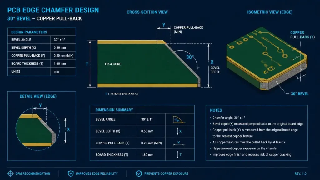
PCB Edge Chamfer & Copper Pull-Back Design Parameters Diagram
PCB gold finger chamfer design requires specifying bevel angle (20°, 30°, 45°, or 60°), bevel depth (calculated from board thickness and residual thickness requirement), and direction (facing away from board center). Standard practice: 30° for general-purpose, 45° for high-insertion-frequency, 20° for maximum contact stability, 60° for minimal insertion force. Inner-layer copper must be removed 0.6–3.0 mm from the board edge under the bevel zone to prevent copper exposure during machining.
Chamfer Angle Selection Matrix
| Angle | Insertion Force | Contact Area | Best Application | Relative Wear |
|---|---|---|---|---|
| 20° | High (1.5–2.0 N/finger) | Maximum | Permanent installations, minimal insertion | Lowest |
| 30° | Moderate (1.0–1.5 N/finger) | Good balance | General-purpose default — 80% of applications | Low |
| 45° | Lower (0.6–1.0 N/finger) | Reduced | High-frequency insertion, hot-swap, DDR5 | Moderate |
| 60° | Very low (0.3–0.6 N/finger) | Minimal | Specialized low-force, guided insertion | Higher |
Hongda Circuit Recommendation: Specify 30° ±2° as the default unless your connector datasheet or application demands otherwise. For server hot-swap modules (PCIe cards, NVMe drives), we recommend 45° to reduce operator insertion force and prevent connector contact damage during rapid maintenance cycles.
Bevel Depth Calculation by Board Thickness
The bevel depth (material removed) is determined by board thickness, chamfer angle, and desired residual thickness:
| Board Thickness (mm) | Chamfer Angle | Residual Thickness (mm) | Bevel Depth (mm) | Bevel Length Along Edge (mm) |
|---|---|---|---|---|
| 1.0 | 30° | 0.5 | 0.29 | 0.58 |
| 1.0 | 45° | 0.5 | 0.25 | 0.35 |
| 1.6 | 30° | 0.5 | 0.78 | 1.56 |
| 1.6 | 45° | 0.5 | 0.55 | 0.78 |
| 2.0 | 30° | 0.65 | 0.78 | 1.56 |
| 2.0 | 45° | 0.65 | 0.68 | 0.96 |
| 2.4 | 30° | 0.7 | 1.04 | 2.08 |
| 2.4 | 45° | 0.7 | 0.85 | 1.20 |
Formula: Bevel Depth = (Board Thickness − Residual Thickness) / tan(Angle)
Critical Design Note: The residual thickness (remaining material at the beveled edge) must be sufficient to prevent board edge cracking during insertion. For standard FR-4, minimum residual thickness is 0.5 mm for boards ≤2.0 mm thick, and 0.65 mm for boards >2.0 mm thick.
Inner-Layer Copper Pull-Back: The Most Violated Rule
During chamfering, the grinding/cutting process exposes the board edge. If inner-layer copper exists beneath the bevel zone, it becomes visible and creates three problems:
- Electrical Short Risk: Exposed copper on the board edge can contact the connector housing or adjacent fingers
- Corrosion Pathway: Exposed copper oxidizes, creating a corrosion migration path into the board interior
- Aesthetic Rejection: IPC-A-600 Class 3 prohibits exposed copper on board edges
Copper Pull-Back Requirements:
| Board Thickness | Minimum Copper Pull-Back from Edge | Notes |
|---|---|---|
| 0.8–1.0 mm | 0.6 mm | Standard clearance for thin boards |
| 1.2–1.6 mm | 0.6–1.0 mm | Most common range; 0.6 mm minimum per IPC |
| 2.0–2.4 mm | 1.0–1.5 mm | Increased clearance for thicker boards |
| 2.4–3.2 mm | 1.5–3.0 mm | Heavy boards; some designs require full copper removal under finger area |
Hongda Circuit DFM Check: Our CAM software automatically flags inner-layer copper within 1.0 mm of any beveled edge. For designs with copper closer than 0.6 mm, we issue an engineering query (EQ) requesting either copper pull-back or written acceptance of exposed copper risk.
Chamfer Direction & Board Edge Orientation
Gold fingers must face outward from the PCB center—the chamfer is always cut on the outer edge of the finger, never between the finger and the board interior. For boards with fingers on multiple edges: • Single-edge fingers: Chamfer faces the board edge containing fingers • Dual-edge fingers (opposite sides): Each edge chamfered independently; confirm panelization does not interfere • Adjacent-edge fingers (L-shape): Requires fully automatic CNC beveling with multi-angle capability; specify angles for each edge explicitly
Common Design Error: Designers occasionally draw the chamfer symbol pointing inward (toward board center) rather than outward. This reverses the bevel direction, creating a sharp edge that damages connector contacts. Always verify chamfer direction against connector insertion orientation.
Conductor Routing, Plating Tie-Bars & Electrical Performance
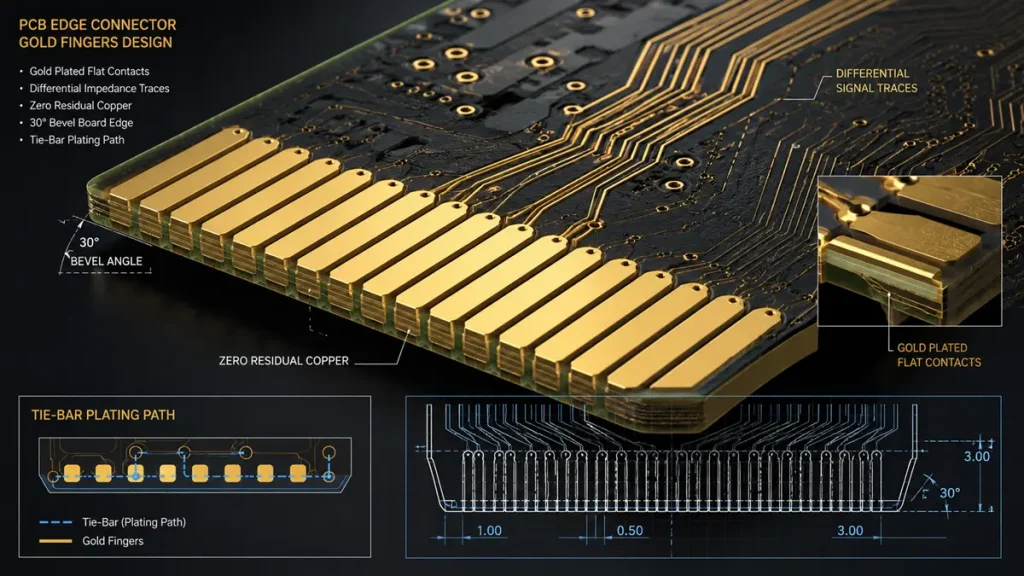
PCB Gold Finger Tie-Bar Plating Path & Differential Trace Routing Diagram
Gold finger PCB conductor routing requires direct trace connection from inner layers to finger pads without stubs or neck-downs. Plating tie-bars (bus bars) must connect all fingers for electroplating current distribution, then be completely removed via routing or V-scoring post-plating—residual tie-bar material causes short circuits. For high-speed designs, maintain impedance continuity through the finger pad, avoid vias within 5 mm of fingers, and ensure continuous ground reference under the finger area.
Trace-to-Finger Connection Best Practices
| Design Rule | Requirement | Rationale |
|---|---|---|
| Trace Width at Finger Pad | Match trace width to pad width; neck-down ≤20% | Prevents impedance discontinuity |
| Trace Entry Angle | 45° or rounded entry; avoid 90° corners | Reduces signal reflection at pad transition |
| Stub Length Beyond Contact Point | <3 mm for PCIe 5.0; <1.5 mm for PCIe 6.0 | Minimizes unterminated transmission line effects |
| Ground Return Path | Continuous ground plane under finger area | Maintains controlled impedance, reduces crosstalk |
| Via-to-Finger Distance | ≥5 mm for high-speed signals | Via stubs create resonant cavities at >16 GHz |
| Differential Pair Routing | Maintain pair symmetry through finger pad | Skew >5 ps degrades eye diagram opening |
| Power Finger Current Density | <10 A/mm² continuous; <20 A/mm² peak | Prevents localized heating and electromigration |
Plating Tie-Bar (Bus Bar) Design & Removal
Since hard gold is electroplated, electrical current must reach every finger pad. This requires plating tie-bars—temporary copper connections between fingers and the panel edge:
Tie-Bar Design Rules:
| Parameter | Specification | Notes |
|---|---|---|
| Tie-Bar Width | 0.5–1.0 mm | Sufficient current capacity for plating bath |
| Tie-Bar Location | Panel edge, outside final board outline | Must not interfere with final board dimensions |
| Connection Point | Finger root (board-edge side) | Minimizes post-removal cleanup |
| Quantity | One tie-bar per finger, or shared bus per row | Shared bus reduces machining but increases plating uniformity risk |
| Removal Method | CNC routing or V-scoring | Routing preferred for clean edges; V-scoring for cost-sensitive designs |
| Residual Requirement | 0.0 mm protrusion beyond board edge | Any residual copper creates short risk and insertion interference |
Hongda Circuit Process: Our Schmoll MX-500 profile router removes tie-bars with ±0.025 mm accuracy, then performs secondary edge polishing to eliminate burrs. For designs requiring absolute zero residual (medical, aerospace), we specify tab routing with mouse-bite breakaway, ensuring the tie-bar breaks flush with the board edge.
Critical DFM Check: Designers must explicitly define tie-bar location in the fabrication drawing. Do not rely on the fabricator to “figure it out”—misplaced tie-bars have caused field failures when residual material shorts adjacent fingers or interferes with connector polarization keys.
Signal Integrity for High-Speed Gold Finger Interfaces
| Parameter | PCIe 5.0 (32 GT/s) | PCIe 6.0 (64 GT/s) | DDR5 (6.4 GT/s) |
|---|---|---|---|
| Data Rate | 32 GT/s | 64 GT/s | 6.4 GT/s (per pin) |
| Nyquist Frequency | 16 GHz | 32 GHz | 3.2 GHz |
| Impedance Target | 85 Ω ±10% diff | 85 Ω ±8% diff | 40 Ω ±10% SE |
| Insertion Loss Budget | <1.5 dB @ 8 GHz | <1.0 dB @ 16 GHz | <0.5 dB @ 3.2 GHz |
| Finger Stub Max | 3 mm | 1.5 mm | 5 mm |
| Via Stub Max | 0.5 mm (back-drilled) | 0.25 mm (blind via) | 1.0 mm |
| Ground Via Density | 1 per signal via | 2 per signal via | 1 per 2 signal vias |
At Hongda Circuit, our signal integrity engineers perform 3D electromagnetic simulation (Ansys HFSS) for all PCIe 5.0/6.0 gold finger designs, optimizing finger pad geometry, trace transition, and ground reference to meet insertion loss and return loss budgets.
PCB Stackup & Layout Guidelines for Gold Finger Regions
Gold finger PCB stackup design requires careful management of layer assignments in the finger region: inner signal layers must route traces to finger pads without crossing splits or voids; ground and power planes must remain continuous under the finger area to maintain impedance control; solder mask and silkscreen must be completely excluded from the finger contact zone (0.5–1.0 mm clearance); and board edge plating (if specified) requires additional copper pull-back and plating tie-bar considerations.
Layer Stackup Recommendations by Application
| Application | Layer Count | Material | Key Stackup Feature |
|---|---|---|---|
| Consumer/Gaming | 4–6 layers | Standard FR-4 (Tg 140°C) | Simple stackup, minimal SI constraints |
| Networking/Server | 8–12 layers | High Tg FR-4 (Tg 170°C) | Dedicated ground planes under finger area |
| AI Server/PCIe 5.0 | 12–16 layers | Low-Dk FR-4 or Megtron 6 | Controlled impedance, back-drilled vias |
| AI Server/PCIe 6.0 | 16–20 layers | Megtron 7 or Rogers 4350B | Ultra-low loss, blind/buried via transitions |
| Military/Aerospace | 6–10 layers | Polyimide or ceramic-filled | High Tg, CTE-matched to connector |
Keepout Zones: Solder Mask, Silkscreen & Component Clearance
| Feature | Minimum Clearance from Finger Pad | Rationale |
|---|---|---|
| Solder Mask Edge | 0.5 mm (20 mils) | Prevents mask encroachment on contact surface; mask residue increases contact resistance |
| Silkscreen/Legend | 1.0 mm (40 mils) | Ink particles contaminate connector contacts; legend must not overlap finger area |
| Plated Through-Hole (PTH) | 1.0 mm (40 mils) | Prevents plating bath contamination; avoids mechanical weak point at edge |
| SMD Pad | 1.0 mm (40 mils) | Prevents solder bridging during assembly; avoids gold contamination from solder paste |
| Component Body | 5.0–15.0 mm | Connector insertion depth determines keepout; reference connector datasheet |
| Copper Pour (Outer Layer) | 0.5 mm | Prevents beveling into copper; maintains insulation |
| Copper Pour (Inner Layers) | 0.6–3.0 mm | Prevents copper exposure during beveling (see pull-back table above) |
Solder Mask Opening Design: The solder mask window for gold fingers must extend 0.5 mm beyond the finger pad edge toward the board edge. This ensures complete mask removal from the contact zone while preventing mask bleed onto the pad during the lamination process. At Hongda Circuit, our LDI solder mask exposure achieves ±0.025 mm registration, ensuring precise mask definition even for 0.5 mm pitch fingers.
Board Edge Plating Considerations
For designs requiring board edge plating (plated board edge for shielding or grounding, distinct from gold fingers): • Edge plating requires an additional plating step after standard fabrication • The plated edge must be separated from gold fingers by minimum 1.0 mm to prevent gold contamination • Edge plating thickness is typically 20–50 μ” copper + 5–10 μ” immersion tin or ENIG • Chamfering of edge-plated boards requires special fixturing to protect the plated edge
DFM Checklist for Gold Finger PCBs: Manufacturing-Ready Design Verification
A gold finger PCB DFM (Design for Manufacturing) review must verify 12 critical parameters before releasing to production: (1) hard gold specification in fab notes, (2) chamfer angle and direction, (3) solder mask clearance ≥0.5 mm, (4) inner-layer copper pull-back ≥0.6 mm, (5) no vias within 1.0 mm of fingers, (6) tie-bar location and removal method, (7) finger pitch tolerance within connector spec, (8) finger length consistency (or intentional long-short), (9) impedance continuity for high-speed signals, (10) component keepout matching connector insertion depth, (11) silkscreen exclusion from finger zone, and (12) panelization compatibility with beveling equipment.
Pre-Release DFM Checklist
| # | Check Item | Pass Criteria | Hongda Circuit Verification |
|---|---|---|---|
| 1 | Hard gold specified | “Electroplated hard gold per IPC-4552, [thickness] μ” over [thickness] μ” electrolytic nickel” in fab notes | CAM engineer confirms spec matches Gerber |
| 2 | Chamfer angle defined | Angle (20°/30°/45°/60°) and direction explicitly stated | Profile compared against mechanical layer |
| 3 | Solder mask clearance | ≥0.5 mm from finger pad edge | Automated DFM software measurement |
| 4 | Silkscreen exclusion | No silkscreen within 1.0 mm of finger | AOI verification on production panels |
| 5 | Inner copper pull-back | ≥0.6 mm from board edge under bevel | Layer-by-layer Gerber analysis |
| 6 | Via exclusion zone | No vias within 1.0 mm of finger pads | DRC check + manual review |
| 7 | PTH exclusion zone | No PTH within 1.0 mm of finger pads | DRC check + manual review |
| 8 | Tie-bar location | Defined on panel edge, outside board outline | CAM review for routing path |
| 9 | Tie-bar removal | Specified method (routing/V-score) | Profile toolpath verification |
| 10 | Finger pitch tolerance | Within ±0.05 mm (standard) or ±0.025 mm (HD) | Measurement on first article |
| 11 | Finger length consistency | All fingers in row within ±0.1 mm (or intentional long-short documented) | Optical measurement |
| 12 | Component keepout | ≥5 mm from board edge (or per connector datasheet) | Assembly drawing review |
| 13 | Impedance control | Trace-to-finger transition simulated (high-speed designs) | TDR verification on qualification coupon |
| 14 | Panelization | Board width ≥45 mm for beveling fixturing; mouse-bite or V-score compatible | Panel layout review |
| 15 | Material specification | Laminate Tg, Dk, Df specified for operating environment | Material certificate verification |
Common Manufacturing Defects & Prevention
| Defect | Root Cause | Design Prevention | Detection Method |
|---|---|---|---|
| Gold flaking/peeling | Insufficient nickel underplate; poor adhesion | Specify ≥200 μ” nickel; require adhesion tape test | Tape test per IPC-TM-650 2.4.18 |
| Chamfer angle deviation | Incorrect machine setup; tool wear | Specify ±0.5° tolerance; request measurement data | Optical angle gauge |
| Copper exposure on edge | Insufficient inner-layer pull-back | Pull back ≥0.6 mm; verify in Gerber review | Visual inspection 10× |
| Solder mask on finger | Mask registration error; insufficient clearance | Design ≥0.5 mm clearance; specify LDI exposure | AOI 100% |
| Tie-bar residual | Incomplete routing; dull cutting tool | Specify flush removal; require edge inspection | Visual + tactile inspection |
| Plating thickness non-uniformity | High aspect ratio; insufficient agitation | Specify pulse plating; limit finger length to <40 mm | XRF 5 points/finger |
| Contact resistance high | Thin gold; contaminated surface | Specify adequate thickness; require cleanliness test | 4-wire Kelvin measurement |
| Impedance mismatch | Trace neck-down; ground plane void | Maintain consistent trace width; continuous ground | TDR analysis |
Frequently Asked Questions: Gold Finger PCB Design
Is a 30° Chamfer Mandatory for All Gold Finger PCBs?
No. While 30° is the most common default (used in approximately 80% of applications), the optimal chamfer angle depends on insertion frequency, connector specification, and insertion force requirements: • 20°: Use when contact stability is paramount and the board will rarely be removed (embedded systems, permanent backplanes). Higher insertion force but maximum contact area. • 30°: The general-purpose standard. Balanced insertion force and contact area. Suitable for most PCIe, DDR, and industrial applications. • 45°: Use for high-frequency insertion (server hot-swap, test fixtures). Lower insertion force reduces operator fatigue and connector wear. • 60°: Specialized applications only (medical cartridge systems, guided-insertion mechanisms). Very low insertion force but reduced contact area increases wear rate.
Always specify the chamfer angle in your fabrication notes. Never assume the fabricator will select the appropriate angle—this is the #1 cause of gold finger DFM rejections at Hongda Circuit.
Why Can’t Solder Mask Cover the Gold Finger Area?
Solder mask must be completely excluded from the gold finger contact zone for three reasons:
Electrical Insulation: Solder mask is an insulator (dielectric). Any mask residue on the finger surface creates a barrier between the gold plating and the mating connector contact, increasing contact resistance from <20 mΩ to >200 mΩ—effectively an open circuit for low-voltage signals.
Mechanical Interference: Solder mask has a finite thickness (typically 10–25 μm). This thickness prevents the connector contact from seating fully against the gold surface, reducing contact force and creating intermittent connections under vibration.
Mask Degradation: During repeated insertion cycles, solder mask material chips and flakes, generating debris that contaminates the connector housing and adjacent fingers. This debris accelerates wear and can cause short circuits between closely spaced fingers.
Design Rule: The solder mask opening must extend 0.5 mm beyond the finger pad edge toward the board edge. This ensures complete mask removal while providing a small buffer against mask registration errors.
How Should Plating Tie-Bars Be Designed and Removed?
Plating tie-bars (bus bars) are temporary copper connections required to distribute electroplating current to all gold finger pads. They are removed after plating but require careful design to prevent field failures:
Design Rules: – Location: Tie-bars must be placed on the panel edge, outside the final board outline. Never place tie-bars within the board profile. – Width: 0.5–1.0 mm per finger, or a shared bus of 2.0–3.0 mm width for an entire finger row. – Connection Point: Connect at the root of the finger (the board-edge side), not the tip. This minimizes the residual stub after removal. – Removal Method: Specify either CNC routing (cleanest, ±0.025 mm accuracy) or V-scoring (lower cost, slight residual nub).
Post-Removal Verification: After tie-bar removal, the board edge must be inspected for: – Residual copper protrusion: 0.0 mm tolerance—any protrusion interferes with connector insertion – Burrs: Must be removed by secondary polishing; burrs damage connector contacts – Gold plating integrity: Removal process must not chip or peel the gold layer
At Hongda Circuit, our Schmoll MX-500 profile router with diamond-coated tools removes tie-bars with zero residual protrusion, followed by automated edge polishing to Ra <0.4 μm. For designs requiring absolute zero residual (medical, aerospace), we specify tab routing with mouse-bite breakaway, ensuring the tie-bar breaks flush with the board edge.
Why specify Electroplated Hard Gold instead of ENIG for gold fingers?
Edge connectors require Electroplated Hard Gold (IPC-4552) with cobalt alloy (130–200 HK) to withstand 1,000+ insertion cycles. ENIG (immersion gold, 50–70 HK) wears off within 1–10 cycles, leading to nickel oxidation and contact failure. ENIG is strictly prohibited for gold fingers.
How do I request a fast PCB quotation and DFM review?
Submit Gerber files, stackup, and fab notes specifying IPC-4552 hard gold thickness, chamfer angle (30°/45°), and impedance targets (e.g., 85Ω for PCIe 5.0).
DFM Review: 4–8 hours
Standard Lead Time: 5–7 working days
Shenzhen Hongda Circuit Technology Co., Ltd. | Email: engineering@hongdacircuit.com
About Author
David Chen https://www.linkedin.com/in/pcbcoming
David Chen boasts an extensive professional background in PCBA manufacturing, PCBA testing, and PCBA optimization, with specialized expertise in high-precision PCBA fault analysis and rigorous PCBA reliability testing. The author has worked with high-layer-count server PCB fabrication, ultra-low-loss backplane stackups, and thermo-mechanical reliability optimization for AI infrastructure projects involving 112G and 224G PAM4 architectures. Skilled in complex circuit design and cutting-edge advanced PCB manufacturing processes, he delivers solutions that elevate product durability and performance across industrial applications. His technical articles focusing on PCBA manufacturing workflows and testing methodologies are widely cited by industry peers, research institutions, and technical platforms, solidifying his reputation as a recognized technical authority in the global circuit board manufacturing sector.