Custom LED PCB Manufacturing: From 24-Hour Prototypes to Scalable Production at Shenzhen Hongda Circuit Technology
When a lighting OEM in Stuttgart needed to validate a new high-bay LED driver design in under three days, or when an automotive tier-one supplier in Detroit demanded zero-defect aluminum PCBs for a headlamp program, the underlying question was identical: Can this LED PCB manufacturer move as fast as our product roadmap demands—without compromising thermal performance or assembly yield?
At Shenzhen Hongda Circuit Technology Co., Ltd., we built our custom LED PCB manufacturing service around that exact tension. Our facility in Shenzhen operates as a dedicated LED PCB factory for engineers and procurement teams who refuse to choose between speed, thermal integrity, and scalable volume. Whether you need a single aluminum PCB prototype for thermal validation or a 50,000-square-meter annual production run with full turnkey assembly, the same engineering team, the same SMT lines, and the same AOI protocols apply.
This page explains how we solve the five most expensive problems in LED electronics procurement—slow prototyping, thermal design failures, opaque quality control, rigid sourcing models, and capacity bottlenecks—through a manufacturing system that combines 2026-grade process technology with procurement flexibility.
Rapid LED PCB Prototyping: 24–72 Hour Turnaround for Time-Critical Programs
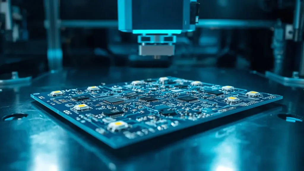
Custom LED PCB Assembly & Automated Inspection at Hongda Circuit
Why 72 Hours Is the New Industry Baseline for LED PCB Prototypes
The shift toward modular lighting architectures and shorter product lifecycles has compressed prototype cycles from weeks to days. A custom LED PCB that once required two weeks for fabrication and assembly now needs to ship within 72 hours to keep a lighting fair demo or automotive PPAP schedule on track.
At Hongda Circuit, our rapid LED PCB prototyping workflow is structured around three velocity tiers:
- 24-hour express: Single-layer aluminum PCB or double-layer FR-4 LED boards, pre-approved Gerber, no DFM revisions required. Ideal for thermal proof-of-concept builds.
- 48-hour standard: Multi-layer LED PCB prototypes (up to 8 layers) with standard copper weight and ENIG surface finish. Suitable for electrical validation before pilot runs.
- 72-hour complex: High-density interconnect (HDI) LED boards, mixed aluminum-FR-4 constructions, or designs requiring heavy copper (3–4 oz) for automotive current loads.
What “Fast” Actually Means: Engineering Review, Not Just Machine Speed
Speed without accuracy is expensive. Every prototype order enters a parallel-process DFM review where our engineers validate thermal via placement under LED footprints, solder mask registration for white-reflective coatings, and stencil aperture ratios for high-power LED packages. We do not sacrifice DFM for velocity; we run both simultaneously.
Materials available for prototype builds:
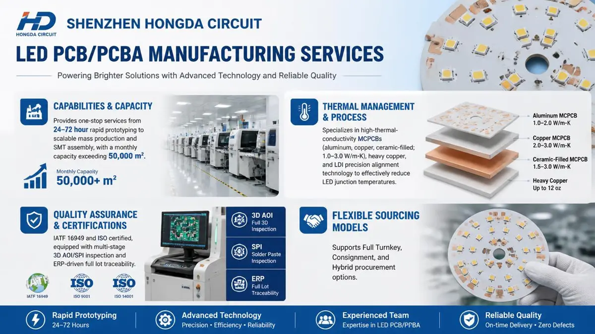
- High-thermal-conductivity aluminum substrates (1.0–3.0 W/m·K dielectric)
- Standard FR-4 with thermal via arrays
- Flexible LED strip substrates (polyimide-based)
- Ceramic-filled MCPCB for UV and horticultural lighting
Scalable LED PCB Manufacturing Capacity: From Pilot Run to Mass Production Without Switching Factories
The Procurement Trap: Prototype in One Facility, Mass-Produce in Another
One of the most disruptive hidden costs in LED electronics sourcing is the factory transfer gap. A prototype built in a quick-turn shop rarely scales cleanly to a volume factory because stencil designs, reflow profiles, and even copper etch tolerances differ. The result: requalification delays, color-temperature drift, and unexpected field failures.
Hongda Circuit eliminates that gap. Our LED PCB manufacturing floor is configured for seamless volume ramping:
| Capability | Specification |
|---|---|
| Monthly PCB fabrication capacity | 50,000+ square meters |
| Layer count | 1–16 layers (LED-optimized stackups) |
| Maximum panel size | 600 × 700 mm |
| Copper weight range | 1 oz – 6 oz (heavy copper for automotive LED drivers) |
| Thermal substrate types | Aluminum core, copper core, ceramic-filled MCPCB |
Batch Traceability as a Default, Not an Upgrade
For procurement teams managing automotive or medical lighting programs, traceability is non-negotiable. Our ERP system assigns unique lot IDs at the raw-material receiving stage (IQC) and tracks each panel through etching, lamination, drilling, plating, solder mask, and final electrical test. If a field failure occurs three years post-delivery, we can trace it back to the specific prepreg roll, copper foil batch, and SMT feeder slot.
Advanced SMT Assembly Lines: Built Specifically for LED and Automotive Lighting
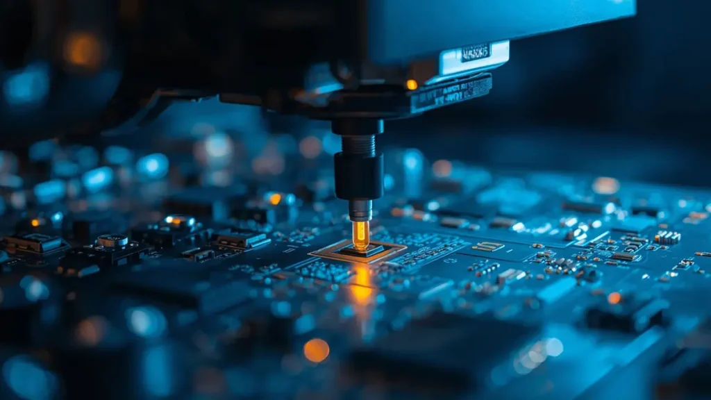
High-Precision SMT Pick-and-Place Assembly at Hongda Circuit
Why Standard SMT Lines Struggle with LED Boards
A generic SMT line optimized for consumer electronics will mishandle aluminum PCBs. The metal substrate alters reflow thermal mass, causing cold joints on large copper pours or tombstoning on small 0603 LEDs. The stencil aperture that works for a smartphone motherboard will deposit too much paste under a 3535 high-power LED, creating solder bridging that AOI misses until functional test.
Hongda Circuit operates dedicated LED SMT assembly lines with process parameters tuned for thermal substrates:
Equipment Profile:
- High-speed pick-and-place: Yamaha YSM series, placement accuracy ±25 µm at 3σ, supporting 0201 through BGA and LED packages from 0603 to 7070 COB.
- Multi-zone reflow ovens: Heller 1913 MK7 with nitrogen atmosphere and closed-loop thermal profiling. Profile recipes are stored per substrate type—aluminum PCBs receive slower ramp rates above 200°C to prevent dielectric delamination.
- 3D SPI (Solder Paste Inspection): Koh Young KY8030-3, measuring paste volume, height, and area per pad before component placement. This catches insufficient paste under thermal pads before the LED is placed.
- LED-specific stencil design: Laser-cut stepped stencils with reduced aperture ratios (0.55–0.60 area ratio) under high-power LED thermal pads to prevent excessive solder squeeze-out.
Turnkey LED PCB Assembly: Component Sourcing Without the Headaches
Our turnkey LED PCB assembly service covers the full procurement chain: BOM scrubbing, alternate component recommendations (especially for constrained LED drivers and MOSFETs), incoming material inspection, and kitting to the SMT line. For automotive clients, we maintain a preferred-vendor list of AEC-Q100/Q101-qualified components and can source through authorized distributors with full counterfeit-mitigation documentation.
Multi-Stage AOI and Quality Assurance: Catching Defects Before They Leave the Building
Beyond Visual Inspection: The Economics of Zero Escape
In LED lighting, a single reversed polarity on a high-power LED string or a marginal cold solder joint on a thermal pad does not fail immediately. It fails six months later in a sealed fixture, triggering a warranty claim that costs 40× the board price to resolve. That is why Hongda Circuit treats AOI not as a checkbox, but as a layered defense system.
Our inspection architecture:
- Pre-reflow 3D AOI: Omron VT-S730 series, inspecting component presence, polarity, and placement offset immediately after pick-and-place. Polarity verification is critical for LEDs—our algorithm compares the cathode-mark orientation against the centroid data for every diode.
- Post-reflow 3D AOI: Koh Young Zenith Alpha, measuring solder joint volume, fillet shape, and bridging. For aluminum PCBs, we run a secondary algorithm trained on MCPCB reflectance profiles to reduce false calls from the metal substrate glare.
- X-Ray Inspection (Optional): Nikon’s XT V 160 system for BGA and QFN packages on LED driver boards, verifying void percentages under thermal pads.
- Electrical Testing: Flying probe (Takaya APT-1400F) for prototypes; bed-of-nails ICT for volume runs, testing LED forward voltage, driver output stability, and insulation resistance.
Defect Data as a Process Improvement Tool
Every AOI image is archived. If a defect trend emerges—say, a 2% tombstone rate on a specific 0402 LED after the third shift—we trace it to the reflow zone profile or feeder calibration and adjust before the next lot. Our current first-pass yield for LED assemblies exceeds 98.5%, and our field return rate for automotive lighting programs is below 10 PPM.
Flexible Manufacturing Models: Turnkey, Consignment, and Hybrid Engagement
Procurement Flexibility for Different Supply Chain Maturities
Not every buyer wants the same relationship with their LED PCB factory. We structure engagements around three models:
Turnkey LED PCB Manufacturing You send the Gerber and BOM; we handle PCB fabrication, component procurement, assembly, testing, and logistics. Best for teams without in-house sourcing bandwidth or those launching new products where component selection is still fluid. We provide DFM feedback that often reduces BOM cost by suggesting pin-compatible alternates or consolidating package types.
Consignment Assembly (Consigned Materials) You supply the critical components—often the LED emitters, driver ICs, or proprietary sensors—and we provide the PCB, passive components, and assembly labor. This model is preferred by automotive and medical lighting firms who control their semiconductor supply chain directly. Our IQC lab verifies your incoming materials against datasheets before they enter the SMT line.
Partial Turnkey (Hybrid) A practical middle ground: you consign the high-value or long-lead components, and we procure the standard passives, connectors, and mechanical hardware. This balances cost control with procurement efficiency.
Transparent Order Tracking
Regardless of the model, every client receives access to our production portal, showing real-time WIP status, inspection photos, and shipping documentation. No email chasing. No black-box manufacturing.
2026 Manufacturing Technology: What Separates a Competitor from a Partner
Laser Direct Imaging (LDI) for Fine-Pitch LED Arrays
Traditional film-based exposure struggles with the registration tolerances required for fine-pitch LED packages (≤0.4 mm pitch) on aluminum substrates. Hongda Circuit has deployed Laser Direct Imaging (LDI) on our MCPCB lines, eliminating phototools and achieving ±8 µm layer-to-layer registration. This matters when you are routing 3-mil traces between thermal vias under a high-density COB LED.
Next-Generation Thermal Dielectric Materials
We have qualified ceramic-filled prepreg systems with thermal conductivity ratings of 2.0–3.0 W/m·K—nearly double the industry-standard 1.5 W/m·K. For a 10W LED array, this material upgrade can reduce junction temperature by 8–12°C, directly extending lumen maintenance life.
Heavy Copper and Thermal Via Integration
Automotive LED modules running at 2–3A per channel require more than standard 1-oz copper. Our plating lines support up to 6-oz copper weight with filled and capped thermal vias, creating low-resistance thermal and electrical paths from the LED pad to the aluminum core.
Smart Factory Integration
While not yet a client-facing feature, our MES (Manufacturing Execution System) integration with AOI and SPI machines enables predictive quality alerts. If paste volume on a specific pad drifts by 15% across three consecutive panels, the system flags the stencil for cleaning before a defect is produced.
LED PCB Applications We Engineer For
Our custom LED PCB manufacturing capability spans the full lighting spectrum:
- Commercial & Architectural Lighting: Panel lights, downlights, linear fixtures, and tunable-white systems requiring consistent CCT across batches.
- Automotive Lighting: Daytime running lights (DRL), headlamp modules, tail lamps, and interior ambient lighting—built to IATF 16949 disciplines.
- Industrial & Horticultural Lighting: High-bay fixtures, grow lights with specific PAR spectrum requirements, and UV-C sterilization systems.
- Display & Signage: Indoor and outdoor LED modules, fine-pitch LED screens, and transparent LED film applications.
- Medical & Specialty: Surgical lighting with high CRI requirements and dental curing lights with precise irradiance control.
Why Procurement Teams Choose Hongda Circuit as Their LED PCB Factory
- Single-facility prototype-to-production: No requalification when you scale from 10 pieces to 10,000.
- Thermal engineering support: We do not just build your file; we review thermal via strategy, copper weight, and solder mask reflectivity for your specific LED package.
- Automotive-grade quality systems: IATF 16949, ISO 9001, and ISO 14001 certified. PPAP documentation available on request.
- Flexible commercial terms: Turnkey, consignment, or hybrid—structured around your cash-flow and inventory preferences.
- Direct engineer access: Your project is managed by a dedicated application engineer, not a generic sales inbox.
Frequently Asked Questions
How do I choose between turnkey and consignment LED PCB assembly?
Choose turnkey if you lack component sourcing infrastructure or are in early-stage development where BOMs change frequently. Choose consignment if you have established semiconductor relationships, need to protect proprietary LED emitter sources, or are managing automotive programs with mandated supplier lists. Most of our clients start turnkey for prototypes and migrate to partial consignment at volume.
What is the fastest lead time for a custom aluminum PCB prototype?
For single-layer aluminum PCBs with standard 1.6 mm thickness and ENIG finish, we offer 24-hour fabrication plus same-day SMT assembly if components are in stock. Complex multi-layer MCPCB or heavy-copper designs typically require 48–72 hours. The key variable is DFM clarity—Gerbers with complete stackup notes and drill files move through our pre-production queue faster than packages requiring engineering queries.
How does AOI inspection prevent field failures in LED lighting?
AOI catches three failure modes that are invisible to manual inspection but catastrophic in the field: LED polarity reversal (causes entire strings to fail), insufficient solder under thermal pads (causes junction temperature rise and premature lumen depreciation), and solder bridging between driver output pins (causes short-circuit failures). Our post-reflow 3D AOI archives every image, creating a traceable quality record for warranty defense.
What certifications should I verify before selecting an LED PCB manufacturer for automotive lighting?
Minimum: ISO 9001 (quality management) and ISO 14001 (environmental). For automotive: IATF 16949 is mandatory. For North American markets: UL listing (UL 796 for PCBs, UL 94 V-0 for flammability). For European markets: RoHS 3 and REACH compliance. Hongda Circuit maintains all of the above, and we provide material composition declarations and PPAP Level 3 documentation for automotive clients.
Can an LED PCB factory handle both rapid prototyping and high-volume mass production?
Many cannot. The equipment, staffing model, and process control required for 24-hour prototyping (flexible setup, small batches, rapid NPI) differ fundamentally from high-volume manufacturing (automated material handling, dedicated lines, statistical process control). Hongda Circuit operates both models under one roof with shared engineering and quality systems, eliminating the requalification risk that occurs when you transfer from a prototype shop to a volume factory.
Ready to move your LED PCB project from concept to production?
Shenzhen Hongda Circuit Technology Co., Ltd.
Website: www.pcbkr.com
Email: sales@pcbkr.com
About Author
David Chen https://www.linkedin.com/in/pcbcoming
David Chen boasts an extensive professional background in PCBA manufacturing, PCBA testing, and PCBA optimization, with specialized expertise in high-precision PCBA fault analysis and rigorous PCBA reliability testing. The author has worked with high-layer-count server PCB fabrication, ultra-low-loss backplane stackups, and thermo-mechanical reliability optimization for AI infrastructure projects involving 112G and 224G PAM4 architectures. Skilled in complex circuit design and cutting-edge advanced PCB manufacturing processes, he delivers solutions that elevate product durability and performance across industrial applications. His technical articles focusing on PCBA manufacturing workflows and testing methodologies are widely cited by industry peers, research institutions, and technical platforms, solidifying his reputation as a recognized technical authority in the global circuit board manufacturing sector.