Ultra-Thin PCB Price: A 2026 Procurement Decision Framework for Buyers
Ultra thin PCB price is the core question that occupies procurement managers’ minds first and foremost when receiving a PCB stack-up design requiring 0.10 mm finished thickness and 8 μm line/space—far ahead of any technical considerations. Rather than focusing on technical parameters, procurement professionals prioritize a practical financial puzzle: what is the genuine pricing of ultra-thin PCBs, and why do quotations vary drastically across different suppliers?
With fifteen years of experience guiding buyers through full RFQ cycles, covering prototype budgeting for foldable phone camera modules and mass production projects of wearable sensors with millions of pieces, I have concluded that ultra-thin PCB pricing is never a fixed number. It is determined by five core variables that most suppliers conceal in the fine print of quotation documents: layer count, material grade, processing technology, order volume, and the most decisive factor—whether the manufacturer possesses independent professional equipment for stable, mass production of ultra-thin PCBs, or outsources the complex core layer processing to third-party vendors.
This professional guide is tailored for procurement teams, project managers and supply chain engineers. It aims to help practitioners formulate credible and defensible budgets, conduct standardized, comparable evaluation on supplier quotations, and prevent costly unexpected risks that may disrupt ultra-thin PCB projects long after purchase order placement (even up to six months post-order).
Understanding Ultra-Thin PCB Price Drivers in 2026
Before you can negotiate a fair ultra-thin PCB price, you need to understand what drives the number. In 2026, the market has bifurcated into two tiers: factories that treat ultra-thin builds as a standard offering with dedicated lines, and those that run them as exceptions on shared equipment. The price gap between these two tiers is not marginal—it is often 40–120% at prototype volumes and 20–50% at mass production.
How Layer Count and Board Thickness Impact Ultra-Thin PCB Cost
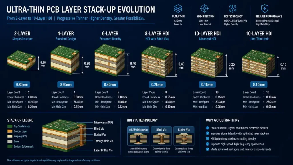
Ultra-Thin PCB Layer Stack-Up Evolution & Thickness Progression
The relationship between layer count and ultra-thin PCB manufacturing cost is non-linear. A 2-layer board at 0.20 mm is a routine build. A 4-layer board at the same thickness requires sequential lamination, thinner prepreg, and significantly tighter registration. A 6-layer build below 0.30 mm enters territory where standard subtractive etching becomes unreliable.
Here is what the 2026 market looks like for buyers:
| Build Specification | Prototype Price (5–10 pcs) | Mass Production (10K+ pcs) | Key Cost Driver |
|---|---|---|---|
| 2-layer, 0.20 mm, standard FR-4 | $40–$150 per order | $1.00–$3.00 per piece | Material yield, panel utilization |
| 4-layer, 0.20 mm, ENIG finish | $80–$300 per order | $2.50–$5.00 per piece | Sequential lamination, registration |
| 6–8 layer, HDI, ≤0.30 mm | $150–$1,000+ per order | $5.00–$15.00 per piece | Laser drilling, mSAP, impedance testing |
| 10+ layer, Any-Layer HDI, 0.10–0.15 mm | $500–$3,000 per order | $8.00–$25.00 per piece | Stacked microvias, ultra-thin copper, yield loss |
Source: Internal production data, Shenzhen Hongda Circuit Technology, 2024–2026.
The jump from 2-layer to 4-layer is roughly 80–150% at prototype stage. The jump from 4-layer standard to 4-layer HDI is another 200–400%. This is not markup. It is the reality of process steps: laser drilling adds cycle time, mSAP imaging requires dedicated chemistry lines, and impedance control demands TDR testing that standard boards never see.
At Shenzhen Hongda Circuit Technology Co., Ltd., our dedicated ultra-thin line handles builds down to 0.10 mm finished thickness with 12-layer capability in mass production. We run SCREEN Ledia LDI direct imaging at 8 μm resolution and Mitsubishi UV/CO₂ hybrid laser drilling at 75 μm microvia diameter with ±5 μm positional accuracy. These are not marketing specifications—they are the thresholds that separate a quoted price you can rely on from one that balloons after the first article fails electrical test.
Material Selection and Its Effect on Ultra-Thin PCB Manufacturing Cost
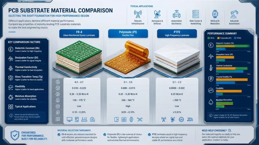
PCB Substrate Material Comparison: FR-4 vs Polyimide vs PTFE
Material is where most buyers lose control of their budget. Standard FR-4 thinned to 0.10–0.20 mm core is the baseline. But if your application requires high Tg for automotive under-hood use, polyimide for flexible sections, or PTFE blends for 5G mmWave, the material multiplier changes everything.
| Material Category | Cost Multiplier vs. Standard FR-4 | Typical Application |
|---|---|---|
| Standard FR-4 (thin core, ≤0.20 mm) | 1.0× | Consumer electronics, LED strips |
| High Tg FR-4 / Halogen-free | 1.15–1.30× | Automotive, industrial control |
| Polyimide (PI) flexible substrate | 2.0–3.0× | Wearables, medical patches, foldable devices |
| LCP (Liquid Crystal Polymer) | 2.5–4.0× | High-frequency flexible, 5G antenna modules |
| PTFE / Modified epoxy (RF-grade) | 3.0–5.0× | Radar, 6G infrastructure, AI server backplanes |
The polyimide premium is particularly relevant for procurement teams sourcing ultra-thin flexible PCB builds. At 0.08–0.15 mm total thickness, PI substrate alone can represent 35–50% of the raw material cost. If your design does not actually require dynamic flexing—only thinness—specifying PI when thinned FR-4 would suffice adds unnecessary cost without functional benefit.
Our engineering team at Hongda Circuit provides complimentary stack-up reviews to flag these material mismatches before tooling begins. In 2025 alone, we identified $180,000 in avoidable material upgrades across 23 customer programs simply by substituting high-Tg FR-4 for PI in static-flex applications.
Ultra-Thin PCB Quotation Guide: What Buyers Must Know Before RFQ
A well-structured RFQ is the difference between receiving three comparable quotes and receiving three numbers that describe entirely different products. Here is what every procurement manager should include when requesting an ultra-thin PCB quotation.
Prototype vs. Mass Production: Ultra-Thin PCB Price Per Unit Breakdown
The most common budgeting error I see is using prototype unit cost to estimate mass production. The curves do not scale linearly.
Prototype Phase (5–50 pcs):
- NRE and tooling dominate. For a 4-layer HDI build with mSAP, expect $200–$500 in non-recurring engineering fees.
- Panel utilization is poor. A 0.15 mm board cannot be panelized as aggressively as 1.6 mm stock because handling damage risk increases exponentially below 0.30 mm.
- Test coverage is higher. Every prototype at Hongda Circuit undergoes 100% flying probe test plus 3D X-ray on microvias. This adds $30–$80 per order but eliminates field failures.
Mass Production (1K–50K pcs):
- NRE amortizes to near zero.
- Panelization efficiency improves 40–60% as process engineers optimize breakaway tabs and tooling rails.
- Test strategy shifts from 100% flying probe to AOI + sampling TDR, reducing per-unit test cost by 70%.
| Volume Tier | 4-Layer Ultra-Thin (0.20 mm) | 6-Layer HDI (0.30 mm) |
|---|---|---|
| 5–10 pcs (prototype) | $8–$30 per piece | $15–$100 per piece |
| 100–500 pcs (pilot) | $5–$15 per piece | $10–$30 per piece |
| 1,000–5,000 pcs | $3–$8 per piece | $5–$15 per piece |
| 10,000+ pcs | $1.50–$3.50 per piece | $3–$8 per piece |
Note: Pricing assumes standard FR-4, ENIG finish, and ≤1 oz copper. High-frequency materials, heavy copper, or ENEPIG will shift these ranges upward.
Hidden Costs That Inflate Your Ultra-Thin PCB Budget
Experienced buyers know to look beyond the line-item PCB cost. Here are the five hidden cost drivers that destroy budgets:
1. Impedance Control Surcharges When trace widths drop below 75 μm, impedance tolerance tighter than ±10% requires TDR validation on every lot. At Hongda Circuit, we include this in our standard HDI quotation. Many competitors add $50–$150 per lot as a “special test fee” after order confirmation.
2. Warpage Rework Boards below 0.20 mm warp during reflow if lamination pressure profiles are not optimized. A factory without vacuum lamination (ours runs LAUFFER presses at <50 mbar) will ship boards that your SMT line rejects. The cost of stripping, re-laminating, and re-plating is rarely absorbed by the fabricator.
3. Microvia Void Failures Stacked microvias in ultra-thin builds are susceptible to voids if desmear chemistry is too aggressive. Our plasma cleaning system uses CF₄/O₂ chemistry instead of permanganate, eliminating over-etch on thin cores. Factories that outsource laser drilling often lack control over this step.
4. Surface Finish Upgrades OSP is the baseline for cost-sensitive builds. ENIG adds 10–20%. ENEPIG adds 30–60% but is mandatory for wire-bonding and high-frequency applications where skin effect matters. If your RF engineer specified ENEPIG but your buyer quoted ENIG, the redesign cost dwarfs the finish delta.
5. Expedite Fees Standard lead time for 4-layer ultra-thin HDI is 7–10 days. A 3–5 day expedite adds 20–40%. True 24–48 hour turnaround is possible only for simple 2-layer builds and carries a 50–100% premium. We maintain a dedicated quick-turn lane for ultra-thin prototypes with no expedite surcharge up to 48 hours for 2-layer builds.
How Advanced Manufacturing Technology Reduces Ultra-Thin PCB Cost
Here is the counterintuitive truth that procurement teams miss: investing in a factory with better equipment often lowers your total cost, even if the quoted piece price is 10–15% higher than a commodity bidder. The savings come from first-pass yield, reduced rework, faster time-to-market, and elimination of field failures.
mSAP and LDI: Why Equipment Matters for Ultra-Thin PCB Pricing
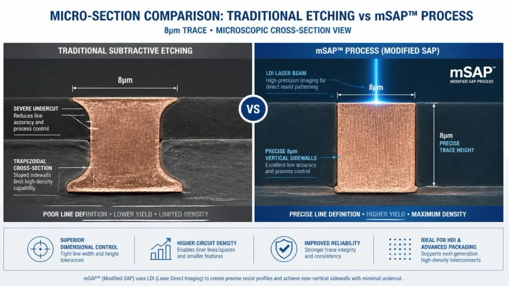
mSAP vs Traditional Subtractive Etching Micro-Section Comparison
Traditional subtractive etching starts with 18 μm copper foil and removes material until traces remain. At line/space below 50 μm, isotropic undercut becomes uncontrollable. A 5 μm variation in trace width shifts characteristic impedance by 2–3 Ω—unacceptable for 224G PAM4 channels or MIPI CSI camera interfaces.
Modified Semi-Additive Process (mSAP) reverses the logic:
- Laminate an ultra-thin 1.5–3 μm copper seed layer.
- Image the trace pattern with LDI at ±1.5 μm accuracy.
- Selectively plate copper to target height (15–20 μm).
- Flash-etch the seed layer.
The result is near-vertical trace sidewalls with minimal undercut, enabling 8 μm/8 μm line/space in production. At Hongda Circuit our mSAP line has been qualified for substrate-like PCB (SLP) builds since 2024.
What this means for your price:
- mSAP eliminates the “design guardband” that forces wider traces and larger vias, saving board area.
- Higher first-pass yield (our AI-inspected ultra-thin line holds >96% yield on 10-layer Any-Layer HDI) reduces scrap allocation in the unit price.
- Direct imaging removes phototool costs and alignment errors, cutting prototype NRE by 30–50%.
In-House vs. Outsourced: The Procurement Risk Factor
The most dangerous word in an ultra-thin PCB supply chain is subcontracted. When a factory outsources laser drilling, mSAP imaging, or impedance testing, three things happen:
- Quality variance: The subcontractor’s process window may not match the prime factory’s stack-up assumptions.
- Lead time inflation: Material moves between facilities, adding 2–4 days and handling risk.
- Opaque pricing: The prime factory marks up subcontracted steps, but you cannot audit the underlying cost.
At Shenzhen Hongda Circuit Technology, we do not subcontract any step of the ultra-thin process. Laser drilling, mSAP imaging, vacuum lamination, plasma desmear, ENIG/ENEPIG plating, 3D X-ray inspection, and 4-port VNA impedance validation all occur within our 12,000 m² Baoan facility. This vertical integration is why we can offer fixed-price prototyping for ultra-thin HDI builds up to 8 layers—something few competitors match.
Ultra-Thin PCB Procurement Strategy: A Step-by-Step Decision Chain
Successful procurement of ultra-thin PCBs follows a six-stage decision chain. Skip any stage, and you introduce risk that manifests as cost overruns or schedule slips.
Stage 1 — Technical Capability Verification
Before requesting a ultra-thin PCB quotation, verify that the supplier has actually built your specification in volume, not just once in a lab.
Request these data points:
- Minimum finished thickness in mass production (not just sample capability)
- Layer-to-layer registration accuracy on builds ≤0.20 mm
- Microvia void rate on stacked structures
- Warpage data after 3× reflow simulation
- Impedance control tolerance with statistical process control (SPC) charts
At Hongda Circuit, we provide a capability alignment document with every quotation that maps your Gerber requirements against our verified production limits. If your design exceeds our mass-production window, we flag it during DFM review—before you commit to tooling.
Stage 2 — Cost Structure Transparency
Demand a line-item breakdown, not a lump-sum number. A transparent ultra-thin PCB price should include:
- Material cost (by laminate type and copper weight)
- NRE / tooling (one-time vs. amortized)
- Process surcharges (mSAP, laser drilling, impedance test)
- Surface finish (OSP, ENIG, ENEPIG, immersion silver)
- Test coverage (AOI, flying probe, TDR, 3D X-ray)
- Packaging and handling (critical for boards <0.20 mm)
We publish this breakdown as standard practice. It allows procurement teams to model volume-price curves and identify where design trade-offs (e.g., reducing from ENEPIG to ENIG) can save 15–20% without functional compromise.
Stage 3 — Risk Mitigation and Delivery Assurance
Ultra-thin boards are fragile. A supplier with excellent process capability but poor logistics will ship you warped or cracked panels.
Evaluate:
- Panelization strategy: Do they use V-scoring or laser depaneling for thin boards?
- Packaging: Are boards shipped in anti-static waffle packs with foam separators?
- Traceability: Can they provide lot-level material certificates and IPC-6012 Class 3 test reports?
- Contingency: Do they hold safety stock of your custom laminate?
Our AI-driven ERP system tracks every panel from laminate receipt through final test, with real-time status updates to customer portals. For medical and automotive programs, we maintain ISO 13485 and IATF 16949 certified lanes with segregated material storage.
Ultra-Thin PCB vs Standard PCB Cost: When Thin Makes Financial Sense
Not every product benefits from going thin. Here is how to evaluate whether the ultra-thin PCB price premium delivers ROI.
Thin pays off when:
- Product thickness is a competitive differentiator (wearables, foldable phones, medical implants)
- Weight reduction improves portability or fuel efficiency (drones, EV battery management systems)
- Thermal path length must be minimized (power modules, LED drivers)
- Bending or flexing is required (robotic joints, catheter electronics)
Thin is unnecessary when:
- The enclosure has 2+ mm of unused vertical space
- The design uses large through-hole components that require mechanical rigidity
- Cost per square centimeter is the primary driver, and function is unaffected by thickness
For context, a standard 2-layer 1.6 mm FR-4 board costs roughly $0.50–$2.00 at volume. An ultra-thin 2-layer 0.20 mm build runs $1.50–$3.50. The 2× premium is justified only if thinness unlocks product features or market positioning that standard thickness cannot.
Frequently Asked Questions (FAQ)
What is the typical ultra-thin PCB price range for a 4-layer prototype in 2026?
For a 4-layer ultra-thin PCB (0.15–0.25 mm finished thickness) with standard FR-4, ENIG finish, and no HDI features, expect $80–$300 for a 5–10 piece prototype order. If your design includes blind/buried vias, impedance control, or mSAP fine-line processing, the range extends to $300–$800. The key variable is whether the supplier owns in-house laser drilling and mSAP capability or subcontracts these steps, which adds 25–40% to the quoted price.
How does mSAP technology affect ultra-thin PCB manufacturing cost?
mSAP (Modified Semi-Additive Process) increases upfront NRE by $200–$500 due to specialized seed-layer lamination and LDI imaging. However, it reduces per-unit cost in three ways: (1) smaller trace geometries allow smaller board area, saving material; (2) near-vertical sidewalls improve impedance consistency, eliminating rework; and (3) higher first-pass yield (>96% at Hongda Circuit) reduces scrap allocation. For volume programs above 5,000 pieces, mSAP typically delivers a 10–20% lower total landed cost than subtractive etching for designs below 50 μm line/space.
Why do ultra-thin PCB quotes vary so much between suppliers for the same Gerber?
Quote variance stems from four factors: equipment ownership (in-house laser/mSAP vs. subcontracted), material sourcing (authorized distributor vs. gray-market laminate), test coverage (AOI-only vs. AOI + TDR + 3D X-ray), and yield assumptions (optimistic first-pass yield vs. conservative scrap allocation). At Hongda Circuit, we provide a capability-alignment document with every quote that shows exactly which process steps apply to your build and why. If a competitor’s quote is 30% lower, ask specifically: Which test steps are omitted? Is laser drilling in-house? What yield assumption is modeled?
What certifications should I verify when sourcing ultra-thin PCBs for medical or automotive applications?
Minimum baseline: ISO 9001:2015 and IPC-6012 Class 3. For medical devices, demand ISO 13485:2016 with documented clean-room lane segregation. For automotive, IATF 16949:2016 is non-negotiable. Aerospace and defense programs require AS9100D. At Hongda Circuit, we maintain all four certifications simultaneously, with production lanes physically segregated by industry. We also provide UL recognition (File E492374) for flame-rated builds. Never accept a generic ISO certificate—request the scope of certification to confirm it covers ultra-thin and HDI fabrication specifically.
How can I reduce ultra-thin PCB cost without compromising reliability?
Five proven strategies: (1) Use thinned FR-4 instead of PI for static-flex applications—saves 50–70% on material. (2) Consolidate impedance-controlled nets to fewer layers to reduce TDR test coverage. (3) Specify ENIG instead of ENEPIG unless wire-bonding or >10 GHz operation is required—saves 15–30%. (4) Design for standard 0.20 mm core thickness instead of custom 0.12 mm if your enclosure allows—the material premium for non-standard cores is 20–40%. (5) Partner with a vertically integrated factory that does not subcontract laser drilling or mSAP—eliminates markup and improves yield. Our DFM team reviews every incoming RFQ for these exact optimization opportunities at no charge.
Ready to Build Your Ultra-Thin PCB Program?
Shenzhen Hongda Circuit Technology Co., Ltd. operates a 12,000 m² facility in Baoan, Shenzhen, with dedicated ultra-thin production lanes qualified to 0.10 mm finished thickness, 12-layer mass production, and 8 μm/8 μm mSAP fine-line capability. We do not subcontract critical process steps, and we publish transparent cost breakdowns with every quotation.
Next Step: Email your Gerber files, stack-up requirements, and reliability targets to sales@pcbkr.com. Our engineering team will return a complimentary DFM review, capability alignment assessment, and detailed ultra-thin PCB quotation within 30 minutes.
Direct Contact:
- Sales & RFQ:sales@pcbkr.com
- Engineering DFM:pcb@pcbkr.com
- Phone: +86 0755 23720053
- Website:www.pcbkr.com
- Address: Room 1608-1610, Research Development Comprehensive Building, Baoyunda Logistics Center, Baoan, Shenzhen, China
© 2026 Shenzhen Hongda Circuit Technology Co., Ltd. All technical data based on internal production test results 2024–2026. Specifications subject to change; contact engineering for latest capability documents.
About Author
David Chen https://www.linkedin.com/in/pcbcoming
David Chen boasts an extensive professional background in PCBA manufacturing, PCBA testing, and PCBA optimization, with specialized expertise in high-precision PCBA fault analysis and rigorous PCBA reliability testing. The author has worked with high-layer-count server PCB fabrication, ultra-low-loss backplane stackups, and thermo-mechanical reliability optimization for AI infrastructure projects involving 112G and 224G PAM4 architectures. Skilled in complex circuit design and cutting-edge advanced PCB manufacturing processes, he delivers solutions that elevate product durability and performance across industrial applications. His technical articles focusing on PCBA manufacturing workflows and testing methodologies are widely cited by industry peers, research institutions, and technical platforms, solidifying his reputation as a recognized technical authority in the global circuit board manufacturing sector.