Ultra-Thin PCB Cost: Why Are Ultra-Thin PCBs So Expensive? A Procurement Engineer’s Guide to Cost Breakdown and Supplier Evaluation
Ultra thin PCB cost often confuses procurement teams during printed circuit board sourcing, especially when pricing differs drastically from standard PCB builds. For a 12-layer rigid board specified with a 0.10 mm finished thickness, procurement engineers frequently receive supplier quotes at four times the cost of a conventional 1.6 mm PCB, with no clear explanation for the massive price gap.
Most buyers rely on basic benchmarking metrics—primarily layer count and board square footage—to evaluate PCB pricing, leading them to label ultra-thin PCB quotations as unreasonably high. However, the core issue lies not in the price level itself, but in the widespread opacity surrounding ultra-thin PCB manufacturing cost drivers. Without a clear grasp of the unique processes, material requirements and production constraints that shape ultra thin PCB cost, procurement teams are unable to conduct data-backed negotiations, verify supplier manufacturing capabilities, or reasonably justify BOM expenses to the finance department.
This guide eliminates the information gap around ultra thin PCB cost and ultra-thin PCB procurement. Compiled from the on-site manufacturing perspective of Shenzhen Hongda Circuit Technology Co., Ltd. (PCBKR), it traces the complete procurement and production decision chain of ultra-thin PCBs, covering raw material selection, core manufacturing processes to final product testing. The guide clearly clarifies key cost expenditure points, common cost-wasting links in production, and how advanced manufacturing equipment and standardized process management stabilize and regularize ultra-thin PCB unit costs for reliable procurement budgeting.
The Ultra-Thin PCB Procurement Decision Chain: What Drives Cost Before You Issue an RFQ
The procurement process for ultra-thin PCBs does not begin with a quote. It begins with a stack-up. Every decision made in the first 48 hours of a project—core thickness, copper weight, via architecture, surface finish—creates cost commitments that are difficult to unwind later. Procurement teams that treat ultra-thin PCB procurement as a late-stage sourcing exercise consistently overpay because they have already locked in expensive constraints.
Understanding the Ultra-Thin PCB Cost Factors That Standard Quotes Hide
A typical PCB RFQ returns a single line-item price per panel or per piece. For ultra-thin builds, that number is almost meaningless without the underlying cost factors:
- Non-standard laminate procurement: Core materials below 0.10 mm are not shelf items. They are custom-pressed with high-Tg resin systems to prevent z-axis expansion during thermal cycling. Lead times stretch to 8–12 weeks, and minimum order quantities (MOQs) from laminate vendors force PCB factories to carry inventory risk that is passed through in material premiums.
- Copper foil uniformity: At Hongda Circuit, we specify 3 μm ultra-low-profile copper foil for sub-0.20 mm builds. Standard 18 μm or 35 μm foils are commodity items; 3 μm foils are not. The thinner the foil, the more sensitive the impedance becomes to thickness variation. A ±2 μm deviation on a 3 μm foil is a 67% tolerance swing. That sensitivity forces tighter incoming inspection and narrower process windows, both of which cost money.
- Stack-up complexity: A 10-layer ultra-thin board with sequential lamination requires three press cycles. Each cycle introduces registration error, resin flow variation, and warpage risk. The procurement decision chain must account for the fact that every additional lamination step is a yield hazard.
If your RFQ does not specify core thickness tolerance, copper profile grade, and lamination cycle count, you are asking suppliers to guess—and they will price in the worst-case scenario.
Ultra-Thin PCB Cost Breakdown: Where Every Dollar Goes on the Factory Floor
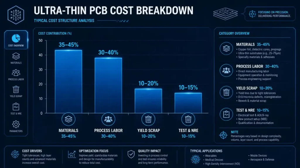
Ultra Thin PCB Cost Breakdown & Structure Analysis – Hongda Circuit
At Hongda Circuit, we break ultra-thin PCB manufacturing cost into four buckets: materials, process labor and machine time, yield loss, and overhead/test. For a typical 8-layer, 0.20 mm build in prototype quantities, the distribution looks roughly like this:
| Cost Bucket | % of Unit Cost (Prototype) | % of Unit Cost (Mass Production) |
|---|---|---|
| Materials (laminate, copper, prepreg, surface finish) | 35–45% | 40–50% |
| Process (drilling, imaging, plating, etching, lamination) | 30–40% | 25–35% |
| Yield Loss & Scrap | 10–20% | 3–8% |
| Test, Inspection, NRE Overhead | 10–15% | 5–10% |
The prototype-to-production gap is instructive. In small batches, fixed NRE and tooling costs dominate. In volume, material efficiency and yield recovery drive the cost down. Procurement engineers who understand this curve can time their sourcing strategy—locking in material prices early for volume, or accepting higher prototype unit costs to avoid redesign risk.
Base Laminate and Ultra-Thin Copper Foil: The Material Cost Premium
Standard FR-4 laminate in 1.6 mm thickness is a commodity. Ultra-thin core laminate is not. For our 0.10 mm minimum rigid builds, we source halogen-free, high-Tg materials from Isola and Panasonic with CTE matched to the copper foil. The material itself costs 2.5–4× standard FR-4, and the thinner the core, the more panels are damaged during handling before they ever reach a drill.
Copper foil selection is equally critical. We maintain inventory of 3 μm and 5 μm ultra-thin copper foils for mSAP (Modified Semi-Additive Process) builds. These foils cannot be handled with standard shop-floor conveyors; they require tension-controlled unwinding systems and clean-room staging to prevent surface oxidation. That infrastructure is not free, and it is not present at every PCB factory.
Microvia Laser Drilling and mSAP Processing: Technology-Driven Process Costs

LDI Laser Direct Imaging & Microvia Drilling for Ultra Thin PCB – Hongda Circuit
Mechanical drilling stops being practical below 0.20 mm via diameters. For ultra-thin HDI boards, laser drilling is mandatory. At Hongda Circuit, our Mitsubishi UV/CO₂ hybrid laser drilling systems achieve 50 μm microvias with ±5 μm positional accuracy. The equipment capital cost is significant, but the operational cost is what procurement teams should watch: laser drilling consumes specialized gases, requires frequent optical calibration, and runs at lower throughput than mechanical drilling.
For fine-line imaging below 30 μm line/space, we deploy SCREEN Ledia LDI (Laser Direct Imaging) systems. LDI eliminates phototools, which is essential for ultra-thin boards because phototools stretch and warp under tension, ruining registration on thin substrates. The trade-off is capital intensity: an LDI line costs 3–4× a standard exposure system, and depreciation is recovered through process fees.
mSAP processing adds another layer. Instead of starting with 18 μm copper and etching away material, mSAP begins with a 1.5–3 μm seed layer, images the trace pattern with LDI, then plates copper to the target height before flash-etching the seed. This near-vertical sidewall geometry is the only way to reliably produce 8 μm/8 μm line/space on ultra-thin builds. It is also slower and more chemistry-intensive than subtractive etching.
Vacuum Lamination and Layer Registration: Yield-Critical Manufacturing Steps
Standard multilayer boards are laminated in hydraulic presses with reasonable tolerance for misalignment. Ultra-thin boards are not. Our LAUFFER vacuum lamination systems operate at <50 mbar vacuum with step-pressure profiling to eliminate air pockets between layers. A single void in a 0.10 mm core can propagate into a delamination during reflow, destroying the board and any components mounted to it.
Registration control is equally unforgiving. We target ±10 μm layer-to-layer alignment on ultra-thin builds. Achieving this requires optical registration systems, thermal compensation algorithms, and panel handling protocols that slow down throughput. A factory without these controls will ship boards that meet electrical test but fail in the field due to microvia fracture or impedance drift.
How Advanced Ultra-Thin PCB Manufacturing Technology Impacts Your Unit Price
Here is a counter-intuitive truth that procurement teams often miss: the factory with the most expensive equipment usually delivers the lowest true unit cost for ultra-thin PCBs. Not because their quoted price is lower, but because their first-pass yield absorbs fewer hidden costs.
Why LDI Direct Imaging and Hybrid Laser Systems Reduce Hidden Defect Costs
Consider the alternative to LDI: conventional phototool exposure. On a standard 1.6 mm board, a 25 μm photool misalignment might still leave an acceptable annular ring. On a 0.15 mm, 10-layer build with 75 μm microvias, that same misalignment creates an open circuit. The board passes electrical test if the crack is partial, then fails after thermal cycling in the customer’s chassis. The cost of that latent defect is not just a replacement board; it is a field failure, a stopped production line, and a damaged supplier relationship.
Our SCREEN Ledia LDI systems, with ±1.5 μm registration accuracy, eliminate this class of defect at the imaging stage. The upfront process cost is higher. The downstream reliability cost is zero. For procurement engineers evaluating ultra-thin PCB suppliers, the question is not “Why is your LDI line more expensive?” It is “What is the cost of the defects your conventional exposure line is not catching?”
Similarly, our Mitsubishi UV/CO₂ hybrid laser drilling platform drills 75 μm blind vias with controlled depth stop. CO₂ lasers ablate dielectric; UV lasers clean copper. The dual-beam approach produces hole walls with minimal resin smear, reducing the desmear process time and improving plating adhesion. Factories using single-wavelength systems or mechanical drilling for larger vias incur higher downstream plating failure rates. Those failures do not appear on the quote; they appear as yield loss that is amortized across all good boards.
From 8 μm mSAP Lines to 3D X-Ray Metrology: Equipment That Pays for Itself in Yield
Hongda Circuit’s mSAP production line is qualified for 8 μm/8 μm line/space—specifications originally developed for substrate-like PCBs (SLP) in smartphone applications. For ultra-thin builds serving AI accelerators and medical imaging, this capability provides headroom. A design calling for 20 μm/20 μm can be manufactured with process margin, not process limits. That margin translates directly to yield.
On the inspection side, our Nordson DAGE 3D X-Ray systems detect voids down to 5% of via barrel volume. For filled microvias in ultra-thin stacks, a 10% void can create a thermal bottleneck that causes layer separation under power cycling. Catching this non-destructively before shipment is cheaper than shipping a latent defect. Our 3D AOI (Automated Optical Inspection) with AI defect classification further reduces escapes by identifying trace geometry deviations at 1 μm precision.
The procurement implication is clear: when you evaluate an ultra-thin PCB supplier, ask for equipment lists and yield data. A factory with laser drills but no 3D X-Ray is drilling blind—literally. A factory with both, and the SPC data to prove stable Cpk values above 1.33, is offering you price predictability that cheaper vendors cannot match.
Ultra Thin PCB Yield and Inspection: The Hidden Cost Multiplier in Your BOM
Yield is the most misunderstood cost driver in ultra-thin PCB manufacturing. A factory quoting $12 per board with 70% yield is actually charging $17.14 per good board. A factory quoting $15 with 95% yield is charging $15.79 per good board. The second supplier is cheaper, but the RFQ rarely exposes this math.
First-Pass Yield vs. Rework: Calculating True Cost Per Good Board
At Hongda Circuit, we track first-pass yield (FPY) by process step for every ultra-thin lot. Typical FPY for a new 0.15 mm, 8-layer design in prototype quantities is 82–88%. By the third production lot, with DFM feedback incorporated, FPY stabilizes above 94%. The 6–12% gap between prototype and production yield is where most procurement budgets bleed.
Why the gap? Ultra-thin substrates warp during etching. Microvias fracture during lamination. Fine lines open during handling. Each defect has a disposition: scrap, rework, or accept. Rework on ultra-thin boards is risky. A repair on a 0.10 mm substrate often introduces more stress than the original defect. We scrap rather than rework when the board is below 0.20 mm, because field reliability data shows reworked thin boards have 3× higher infant mortality. That scrap is real cost, and it is built into the quote.
AOI, X-Ray, and TDR Testing: When Skipping Inspection Becomes the Most Expensive Option
Some buyers request reduced inspection to cut cost. On ultra-thin builds, this is a false economy. Our standard protocol includes:
- 100% AOI after etch and after solder mask, verifying trace width, spacing, and annular ring to 1 μm.
- 3D X-Ray on 100% of microvia panels, checking barrel fill and void content.
- TDR (Time Domain Reflectometry) impedance validation on every production panel, with data archived per IPC-6012 Class 3 requirements.
- Flying probe or grid electrical test verifying 100% netlist coverage.
Skipping any of these steps removes cost from the invoice but adds risk to the supply chain. For medical, automotive, or aerospace ultra-thin programs, that risk is uninsurable. Our advice to procurement teams: do not treat inspection as a line item to be negotiated away. Treat it as insurance with a known premium and an unknown but catastrophic deductible.
NRE, Tooling, and Panel Utilization: Fixed Costs That Disproportionately Affect Small-Batch Ultra-Thin PCB Procurement
Non-Recurring Engineering (NRE) is where small-batch ultra-thin PCB procurement becomes painful. A 4-layer standard board might carry $200 in NRE. A 12-layer, 0.15 mm build with sequential lamination, laser drilling, and impedance testing can carry $2,500–$5,000 in NRE, depending on stack-up complexity.
Engineering DFM Review and Stack-Up Simulation: Upfront Investment or Hidden Savings?
At Hongda Circuit, every ultra-thin RFQ triggers a 24-hour DFM review by our engineering team. We do not charge for this on first articles because we have learned that early intervention prevents expensive surprises. A stack-up that looks fine in simulation may fail in lamination because the prepreg resin flow is incompatible with the core CTE. A via architecture that saves routing space may require an extra lamination cycle that doubles cost.
Our DFM process includes SI/PI simulation for high-speed traces, mechanical bending simulation for rigid-flex hybrids, and thermal modeling for power-dense layers. These are not marketing services; they are technical gates that prevent procurement teams from ordering boards that cannot be manufactured reliably. The cost of a DFM iteration before tooling is negligible compared to the cost of a redesign after first article failure.
Panelization Strategy: How Board Size and Array Design Alter Your Effective Unit Cost
Panel utilization is the silent killer of ultra-thin PCB budgets. A standard 18×24 inch panel might yield 24 pieces of a 2×3 inch board. The same board at 0.10 mm thickness requires larger borders for handling, reduced array density to prevent warpage during reflow, and often a carrier frame for mechanical support during assembly. Effective yield per panel can drop to 16 pieces.
For procurement engineers, the actionable insight is this: ask for the supplier’s panelization plan before accepting the quote. At Hongda Circuit, we provide panel drawings with material utilization percentages as part of every RFQ response. If your board size is inefficient, we will recommend a slight dimension adjustment that improves utilization by 15–20% without affecting functionality. That single change can offset the entire NRE cost in volume.
Volume, Lead Time, and Non-Standard Thickness Surcharges: Budget Variables in the Ultra-Thin PCB Procurement Process
Once design and process are fixed, two external variables dominate ultra-thin PCB cost: quantity and schedule.
Prototype vs. Mass Production: Understanding the Quantity Cost Cliff
The cost curve for ultra-thin PCBs is non-linear. From 5 pieces to 50 pieces, unit cost drops by 30–40% because NRE is amortized over more units. From 50 to 500, the drop is another 20–30% as process parameters stabilize and material MOQs are met. Beyond 1,000 pieces, the curve flattens; the remaining savings come from panel optimization and reduced inspection sampling, not from process breakthroughs.
Procurement teams should plan their sourcing to hit these inflection points. If your program needs 30 prototypes and 200 pre-production units, combining the orders into a single 230-piece lot with staged delivery often costs less than two separate orders, because the process is qualified once and the NRE is paid once.
Rush Orders and Dedicated Line Occupancy: When Speed Demands a Premium
Ultra-thin boards cannot be built on general-purpose lines. Our factory maintains a dedicated thin-board production lane with vacuum lamination, LDI imaging, and controlled-tension handling. When a customer requests 5-day turnaround on a 10-layer, 0.15 mm build, that lane must be cleared of its current lot, re-qualified for the new stack-up, and monitored more intensively. The result is a rush surcharge that reflects real opportunity cost, not arbitrary pricing.
Our recommendation: build standard lead time (10–15 days for prototypes, 3–4 weeks for volume) into your project schedule. If rush is unavoidable, provide the complete data package—Gerber, stack-up, impedance spec, material callouts—on day one. Every day spent clarifying specifications after order placement is a day of schedule risk that converts to expedite fees.
The Ultra-Thin PCB Supplier Evaluation Criteria Every Procurement Team Should Verify
Choosing an ultra-thin PCB supplier is not a price exercise. It is a capability audit. The procurement decision chain should include technical verification steps that go beyond ISO certificates and glossy brochures.
Capability Documents vs. Production Reality: Separating Lab Samples from Volume Manufacturing
Many suppliers can build one perfect 0.10 mm sample in a lab. Few can build 1,000 pieces per month with consistent registration, impedance, and warpage control. When evaluating ultra-thin PCB manufacturers, request:
- Process capability data: Cpk values for critical parameters (registration, impedance, copper uniformity) over the last 12 months.
- Equipment ownership proof: Ask for specific machine models and ages. A 15-year-old laser drill may still function, but its positional accuracy degrades over time. Our Mitsubishi UV/CO₂ systems are maintained under OEM service contracts with quarterly calibration to ±5 μm standards.
- In-house vs. subcontracted processes: If a supplier subcontracts laser drilling, lamination, or impedance testing, they are adding margin and losing control. Hongda Circuit performs all critical processes in-house at our Baoan facility. We do not outsource mSAP, laser drilling, or X-Ray inspection because the interface risk is unacceptable for ultra-thin reliability.
Certifications, Equipment Ownership, and In-House Process Control: The Procurement Checklist
Use this checklist during your next ultra-thin PCB supplier audit:
| Verification Item | What to Ask For | Red Flag |
|---|---|---|
| Minimum rigid thickness | Mass production limit, not sample limit | “We can try 0.08 mm” without yield data |
| Laser drilling capability | Machine model, minimum via diameter, positional accuracy | No UV capability; only CO₂ |
| Fine-line process | mSAP or SAP qualification, minimum L/S | Subtractive etching claimed below 30 μm |
| Lamination control | Vacuum press specification, registration accuracy | Standard hydraulic press for thin cores |
| Inspection depth | 3D X-Ray, AOI, TDR availability | Visual inspection only for microvias |
| Certifications | ISO 9001, IATF 16949, ISO 13485, AS9100D | Generic ISO 9001 only for medical/aerospace builds |
| Traceability | Lot-level material batch records, SPC charts | No data retention beyond shipment |
At Hongda Circuit, we provide this documentation proactively during the qualification phase. Procurement teams that verify these items before placing the first order avoid the most expensive mistake in sourcing: discovering capability gaps after the production lot has failed.
Common Ultra-Thin PCB Cost Myths and Actionable Cost Optimization Strategies
Myth: “Thinner Always Means Cheaper Material” — Why Sub-0.3 mm Builds Defy Intuition
Intuition says less material equals less cost. In PCB manufacturing, the opposite is true below 0.30 mm. The raw laminate is more expensive per square meter. The copper foil is a specialty item. The handling yield is lower. The process time is longer. A 0.10 mm, 8-layer board uses less resin than a 1.6 mm board, but it costs 3–5× as much to produce. Procurement teams must reset this mental model before entering RFQ negotiations.
Design-for-Manufacturing Tactics That Cut Ultra-Thin PCB Cost Without Sacrificing Reliability
Not every ultra-thin PCB cost is fixed. Some are design-dependent and can be optimized:
- Relax line width/space where possible: A design specifying 20 μm/20 μm when 30 μm/30 μm would function eliminates the need for mSAP and allows standard subtractive etching, cutting process cost by 20–30%.
- Minimize sequential lamination cycles: Every additional press cycle adds registration risk and cost. Consolidate layers to reduce lamination steps where electrical performance allows.
- Standardize hole sizes: Using three different microvia diameters instead of one forces multiple laser drill programs and increases setup time. Standardization improves throughput and yield.
- Optimize surface finish selection: ENIG is the default for fine-pitch, but OSP or immersion tin may be sufficient for some ultra-thin applications and cost 15–25% less. Match the finish to the assembly process, not the most conservative option.
- Collaborate on panelization: Allow the manufacturer to adjust board dimensions by ±0.5 mm to improve panel utilization. On a 1,000-piece order, a 15% utilization gain can fund the entire NRE.
At Hongda Circuit, our engineering team provides complimentary DFM feedback with every quotation. We identify these optimization opportunities before tooling begins, giving procurement teams leverage in design reviews.
Conclusion: Transforming “Why Are Ultra-Thin PCBs Expensive?” Into Controllable Procurement Variables
Ultra-thin PCB cost is not a mystery. It is the sum of material premiums, process intensity, yield discipline, equipment depreciation, and fixed NRE amortization. The procurement teams that win in this space are those who stop asking “Why is this so expensive?” and start asking “Which cost drivers can I influence through design, volume planning, and supplier selection?”
The answer, in our experience at Hongda Circuit, is most of them. Stack-up design determines material cost. DFM engagement determines process cost. Supplier capability determines yield cost. Panelization and volume planning determine overhead cost. None of these are outside procurement’s influence; they simply require moving the sourcing conversation upstream, into the design phase.
Shenzhen Hongda Circuit Technology Co., Ltd. has manufactured ultra-thin PCBs down to 0.10 mm finished thickness since 2012. Our Baoan facility operates dedicated thin-board production lines with SCREEN Ledia LDI, Mitsubishi UV/CO₂ hybrid laser drilling, LAUFFER vacuum lamination, and Nordson DAGE 3D X-Ray inspection. We do not subcontract critical processes. We do not guess at yield. We document it, control it, and report it to our customers.
If your next program requires ultra-thin PCBs and you need a supplier evaluation partner who will expose the real cost drivers—not hide them behind a single line-item price—submit your Gerber files and stack-up requirements to sales@pcbkr.com. Our engineering team will return a complimentary DFM review, capability alignment assessment, and detailed cost breakdown within 30 minutes.
Direct Contact:
- Sales & RFQ:sales@pcbkr.com
- Engineering DFM:pcb@pcbkr.com
- Phone: +86 0755 23720053
- Website:www.pcbkr.com
FAQ
What technical capability indicators should I verify when evaluating ultra-thin PCB suppliers for my RFQ?
Focus on four indicators that separate qualified manufacturers from brokers: (1) Minimum mass-production thickness, not sample thickness—ask for yield data on their thinnest production builds. (2) Laser drilling infrastructure—verify they own UV/CO₂ hybrid systems with positional accuracy below ±10 μm, not just mechanical drills. (3) Fine-line process qualification—for sub-30 μm traces, confirm mSAP or SAP capability, not subtractive etching claims. (4) In-house inspection depth—3D X-Ray for microvias and TDR for impedance should be standard, not optional upgrades. At Hongda Circuit, we provide Cpk trend data and equipment calibration records during qualification so procurement teams can verify capability before committing NRE.
Why does my ultra-thin PCB quote vary so much between suppliers for the same Gerber files?
Quote variance usually reflects three hidden differences: yield assumptions, equipment capability, and process ownership. A supplier with 70% assumed yield on a 0.15 mm build must price 43% higher than a supplier with 95% yield to recover the same margin. A supplier subcontracting laser drilling adds a margin layer and loses process control. A supplier without vacuum lamination may quote lower but will struggle with delamination in volume. When comparing ultra-thin PCB quotes, demand a cost breakdown by material, process, test, and NRE—not just a per-piece price. Hongda Circuit provides itemized quotations so buyers can identify exactly where each supplier’s assumptions differ.
How can I reduce ultra-thin PCB cost without switching to a cheaper, lower-reliability supplier?
The most effective cost reductions happen at the design stage, not the negotiation table. Work with your manufacturer on four levers: (1) Relax line/space to the widest dimensions that meet electrical requirements, potentially eliminating mSAP. (2) Reduce sequential lamination cycles by consolidating layers. (3) Optimize panelization to improve material utilization by 15–20%. (4) Standardize hole sizes and surface finishes to minimize setup changes. Hongda Circuit’s DFM team routinely identifies these opportunities during pre-quote review, delivering 10–25% cost reductions without any performance compromise.
What is the real difference between prototype and mass-production cost for ultra-thin PCBs, and when should I lock in pricing?
Prototype ultra-thin PCBs (5–50 pieces) carry high per-unit NRE because engineering review, process setup, and first-article inspection are fixed costs. Mass production (500+ pieces) spreads these costs and benefits from yield stabilization. The transition point is usually 200–500 pieces, where unit cost drops 30–50% from prototype levels. For procurement planning, lock in material pricing 8–12 weeks before production if your design uses non-standard thin cores or low-loss laminates—material allocation risk in 2026 is real, and early commitment secures both price and delivery. Hongda Circuit offers volume pricing tiers and material reservation programs for programs with forecasted demand.
How do I know if a supplier’s claimed ultra-thin PCB capability is real production capacity or just a marketing claim?
Demand evidence, not brochures. Ask for: (a) Recent microsection photographs of boards at your target thickness and layer count, with date stamps. (b) SPC control charts showing registration, impedance, and warpage Cpk over the last 6 months. (c) Equipment asset list with installation dates and calibration records—if they cannot show you the laser drill, they do not own it. (d) Customer references in your industry for volume ultra-thin programs. At Hongda Circuit, we welcome on-site audits and provide full traceability documentation from raw material batch to final test. A factory that resists transparency is a factory that has not actually built what they are selling.
About Author
David Chen https://www.linkedin.com/in/pcbcoming
David Chen boasts an extensive professional background in PCBA manufacturing, PCBA testing, and PCBA optimization, with specialized expertise in high-precision PCBA fault analysis and rigorous PCBA reliability testing. The author has worked with high-layer-count server PCB fabrication, ultra-low-loss backplane stackups, and thermo-mechanical reliability optimization for AI infrastructure projects involving 112G and 224G PAM4 architectures. Skilled in complex circuit design and cutting-edge advanced PCB manufacturing processes, he delivers solutions that elevate product durability and performance across industrial applications. His technical articles focusing on PCBA manufacturing workflows and testing methodologies are widely cited by industry peers, research institutions, and technical platforms, solidifying his reputation as a recognized technical authority in the global circuit board manufacturing sector.