Request Ultra-Thin PCB Quote: A Procurement Decision Chain Guide for Buyers with Gerber-Ready Projects
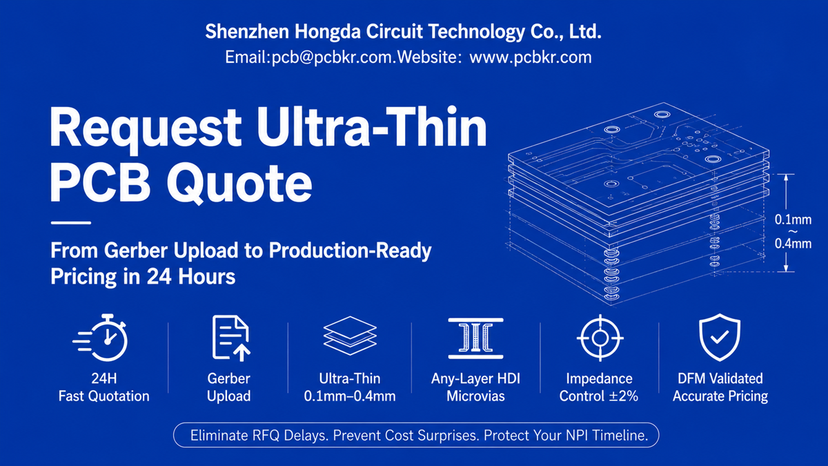
Request Ultra-Thin PCB Quote — From Gerber Upload to Production-Ready Pricing in 24 Hours
Ultra thin PCB quote is the critical, detail-driven result that procurement managers and hardware engineers truly need when they already have finalized Gerber files in hand. At this project stage, generic educational content explaining basic PCB definitions is completely unnecessary. What professionals demand is a custom PCB quotation that strictly complies with real manufacturing constraints, rather than a tentative placeholder estimate that can surge by 40% or more after engineering review.
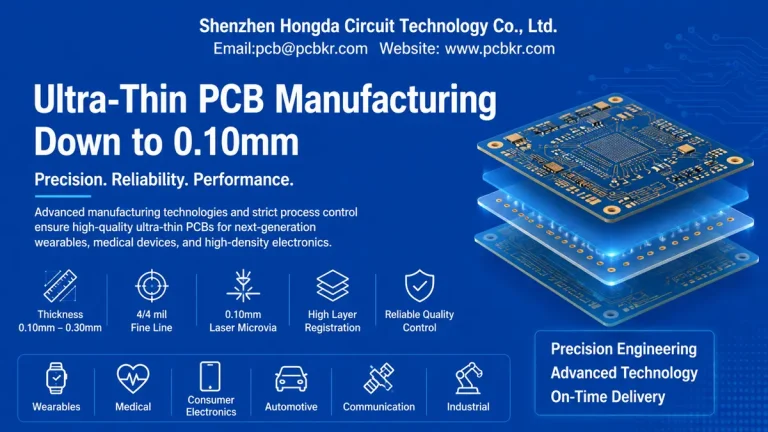
A reliable ultra thin PCB quote must fully cover core customized parameters, including 0.1 mm to 0.4 mm finished board thickness, Any-Layer HDI microvia technology, and impedance-controlled laminates. Most importantly, it needs to be delivered with high efficiency to avoid delays to your entire NPI (New Product Introduction) timeline.
At Shenzhen Hongda Circuit Technology Co., Ltd., we have tailored our ultra-thin PCB quotation workflow exclusively for bottom-of-funnel (BOFU) buyers with mature project documents. You already possess complete stack-up data, drill files and BOM lists—all the essential materials for formal quotation and production verification.
This guide elaborates on the standardized procurement decision process adopted by our professional engineering team. We can convert your RFQ into a fixed, production-ready ultra thin PCB quote within one business day, eliminating repeated communication, ambiguous confirmation and inefficient back-and-forth negotiations that hinder project progress and drag down overall R&D and production efficiency.
How to Get an Accurate Ultra-Thin PCB Quotation: The 4-Step Procurement Decision Chain
Procurement teams sourcing ultra-thin boards face a unique risk profile. Standard PCB quoting engines fail here because 0.2 mm substrates, 75 µm laser microvias, and mSAP fine-line processes do not tolerate generic assumptions. The following decision chain eliminates that risk by forcing technical validation at every stage.
Step 1 — Prepare a Complete Technical File Package Before Submitting Your Custom PCB Quote
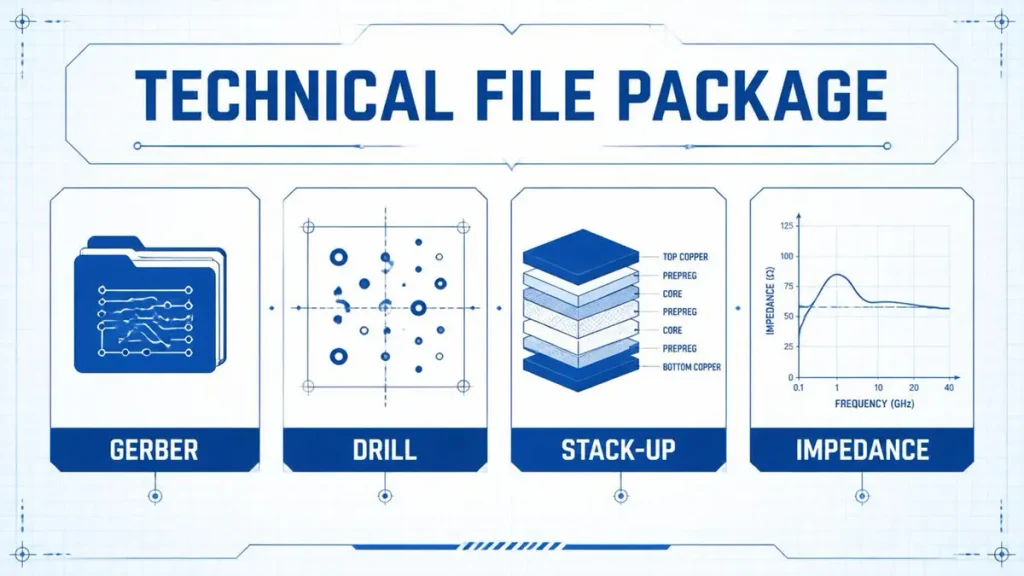
Required Technical File Package for Ultra-Thin PCB Quote Request
The root cause of inaccurate ultra thin PCB quote outcomes is incomplete data. When procurement sends a bare Gerber ZIP without stack-up notes, the supplier must assume standard FR-4, 1.6 mm thickness, and subtractive etching. For ultra-thin builds, those assumptions destroy pricing accuracy.
Hongda’s required RFQ package for thin-board quoting:
- Gerber RS-274X: Current revision copper layers, solder mask, silkscreen, pad master, and board outline in a single ZIP archive.
- NC Drill / Excellon files: Explicitly annotated for plated vs. non-plated holes; critical for thin-core boards where drill wander must be controlled within ±25 µm.
- Stack-up specification: Layer count, finished thickness (0.1 mm–0.4 mm), copper weight per layer, and dielectric material (BT, High-Tg FR-4, or low-loss Megtron 6/7 for high-speed applications).
- Impedance control table: Target impedance, tolerance (we validate ±2% on mSAP lines), and reference layers.
- Surface finish: ENIG, OSP, HASL, or selective hard gold for edge connectors—each carries different cost and lead-time implications on thin substrates.
Procurement pain point solved: You stop receiving “rough estimates” that require re-quoting after DFM review. With a complete package, Hongda’s engineering team runs a preliminary DFM scan before the quote hits your inbox, eliminating the second-round surprise.
Step 2 — Define Quantity Ladders and Project Phase in Your Thin PCB Quote Request
A custom PCB quote for 10 NPI prototypes should not share the same unit economics as a 5,000-piece mass-production run—but it should share the same manufacturing stack-up. Procurement teams often request prototype pricing without declaring downstream volume, which forces suppliers to pad margins against unknown scale.
Hongda’s recommended quantity ladder structure:
- NPI / Prototype: 5–50 pieces; validates stack-up and microvia reliability.
- Qualification / Pre-Production: 100–500 pieces; verifies process capability and yield stability.
- Mass Production: 1,000+ pieces; triggers automated panelization and material volume discounts.
When you submit your ultra-thin PCB quotation request through our portal, the form captures all three tiers simultaneously. Our ERP system then models true unit costs across the product lifecycle, giving procurement a clear view of where scale economies begin.
Step 3 — Receive 24-Hour Engineering Feedback with DFM Optimization for Your Ultra-Thin PCB Quotation
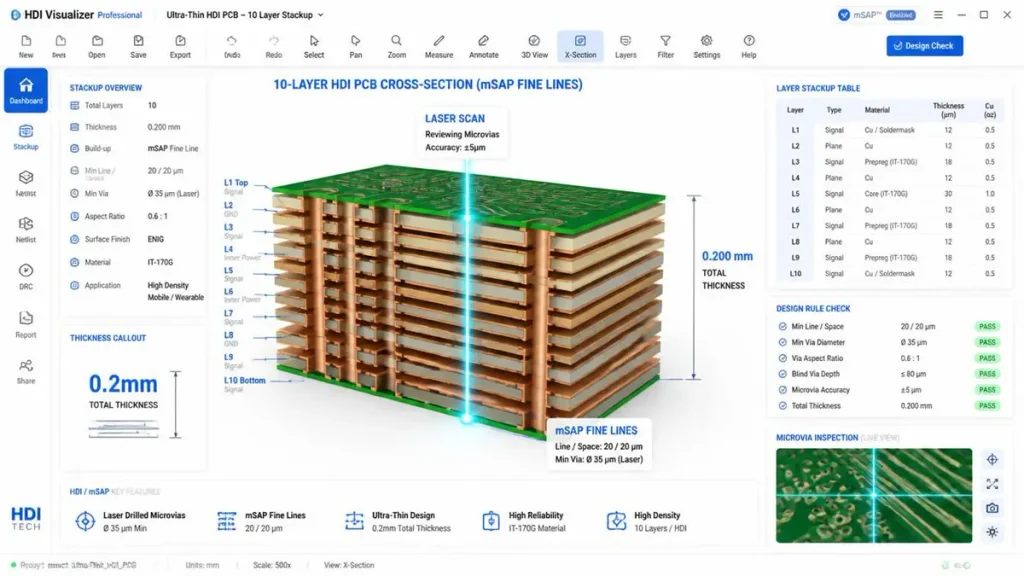
CAD 3D cross-section inspection of an ultra-thin 10-layer HDI PCB stack-up featuring mSAP fine lines (20/20μm) and laser-drilled microvias within a 0.2mm total thickness.
This is where supplier capability separates vendors from partners. Generic PCB brokers return a PDF price list. Hongda returns a technical quote package that includes:
- Locked BOM cost breakdown: Materials, lamination cycles, laser drilling time, mSAP processing, surface finish, electrical test, and logistics.
- DFM risk flags: For example, if your 0.3 mm 10-layer stack-up routes traces between stacked microvias without adequate keep-out, our engineers flag it before you commit tooling.
- Process capability statement: We confirm whether 50 µm line/space is achievable on your specific layer count, or if a design tweak to 60 µm would improve yield by 18% without impacting electrical performance.
Why this matters in 2026: AI server and smartphone camera module projects now demand 224G PAM4 signal integrity on sub-0.4 mm substrates. A quote that ignores via stub length or copper foil roughness is a quote that will fail in the lab. Our ultra thin PCB quotation includes signal-integrity-aware manufacturing notes because our equipment—dual-beam composite laser drills, high-precision LDI, and 3D AI X-Ray inspection—is already qualified for these applications.
Step 4 — Confirm Order and Lock Production Slots with Transparent Lead-Time Contracts
The final procurement decision point is not price alone; it is delivery certainty. In 2026, advanced low-loss laminate lead times have stretched to 16–20 weeks industry-wide. A low thin PCB quote means nothing if the factory cannot secure Megtron 6 or IS415 substrate when your PO arrives.
Hongda’s quote confirmation includes:
- Material allocation status: Real-time inventory of BT, High-Tg, and low-loss laminates.
- Production slot reservation: Confirmed start date upon PO receipt, not “estimated.”
- Logistics option sheet: Standard sea freight, DHL/FedEx/UPS express, or dedicated air freight for time-critical NPI builds.
RFQ Checklist for Thin PCB Quote Requests: Documents That Eliminate Cost Surprises
Use this checklist to audit your own file package before submission. Every unchecked item is a potential source of quote revision.
Mandatory Documents for an Accurate Ultra-Thin PCB Quotation
| Document | Purpose | Common Procurement Gap |
| Gerber RS-274X (.zip) | Copper, mask, silk, outline | Sending outdated revisions; missing solder mask layer |
| Drill files (NC / Excellon) | Hole coordinates and plating spec | No PTH/NPTH annotation |
| Stack-up drawing | Layer sequence, thickness, material | Assuming “standard 1.6 mm FR-4” |
| Impedance requirements | Controlled impedance targets | Missing tolerance spec (e.g., ±5% vs. ±2%) |
| Surface finish spec | ENIG, OSP, HASL, hard gold | Vague “gold plating” request |
| Quantity ladder | Prototype / qual / MP volumes | Only requesting 10-piece price |
Optional but High-Value Additions to Your Custom PCB Quote Package
| Document | Why It Reduces Total Cost |
| Assembly drawing (.pdf) | Clarifies component keep-out zones that affect panelization efficiency |
| Test requirements (ICT, AOI, flying probe) | Prevents post-quote test-scope disputes |
| Compliance needs (IPC Class 3, UL, RoHS, REACH) | Ensures certification costs are built into first article, not added later |
| Panelization preference | Hongda can suggest V-score vs. tab-routing based on your 0.2 mm substrate fragility |
Why Advanced Manufacturing Equipment Directly Impacts Your Ultra-Thin PCB Quotation
Procurement teams often treat PCB quoting as a commodity exercise. It is not. The factory’s equipment list determines whether your 0.3 mm 12-layer board is physically manufacturable at yield, or whether it becomes a months-long rework disaster. Here is how Hongda’s 2026 equipment investments translate into pricing accuracy and risk reduction for your ultra-thin PCB quotation.
Laser Direct Imaging (LDI) and Its Effect on Custom PCB Quote Accuracy
Traditional film-based photolithography introduces alignment errors of ±15 µm—unacceptable when your trace width is 50 µm. Hongda’s LDI systems write patterns directly onto photoresist with sub-5 µm repeatability. For procurement, this means:
- No film tooling charges in your thin PCB quote.
- Fewer imaging-related defects, which means no hidden rework costs passed back as surcharges.
- Faster design-change turnaround: If you rev the Gerber after first article, we re-image without remastering film.
mSAP (Modified Semi-Additive Process) for Ultra-Fine Lines on Thin Substrates
Standard subtractive etching bottoms out at 75 µm line/space. For AI accelerators and 5G-A modules requiring 40 µm traces on 0.25 mm cores, mSAP is the only viable route. Hongda’s mSAP line achieves 15–40 µm geometries with ±2% impedance tolerance.
Procurement impact: If your design requires mSAP, a supplier without this capability will either (a) decline the quote, or (b) attempt it with subtractive etching and deliver opens/shorts. Hongda’s ultra thin PCB quote explicitly confirms mSAP routing when required, with a yield-backed price—no gambling.
Dual-Beam Composite Laser Drilling and 3D AI X-Ray for Microvia Reliability
Any-Layer HDI on ultra-thin boards lives or dies by microvia quality. Hongda deploys dual-beam composite laser drills to create 75 µm blind vias with smooth hole walls—no glass-fiber burrs that cause post-lamination open circuits. Our 3D AI X-Ray inspection then validates stacked via alignment and plating thickness in real time.
Procurement impact: You receive a quote that includes IPC-6012E Class 3 reliability testing as standard, not an upsell. For camera module and wearable device buyers, this eliminates the “via failure in thermal cycling” risk that typically adds 3–4 weeks of failure-analysis delays.
Vacuum Lamination and Plasma Desmear for 0.1 mm–0.4 mm Stack-Ups
Thin-core lamination is where most factories destroy boards. Conventional hot pressing traps air between 0.1 mm cores, creating delamination after five thermal cycles. Hongda’s vacuum lamination equipment eliminates voids, and our plasma desmear process thoroughly cleans resin from microvias before plating.
Procurement impact: Your ultra-thin PCB quotation includes a thermal-shock guarantee (tested to 20 cycles per IPC-TM-650) because our process controls make it repeatable, not aspirational.
CTA Form Design: How to Structure a High-Conversion RFQ for Ultra-Thin PCBs
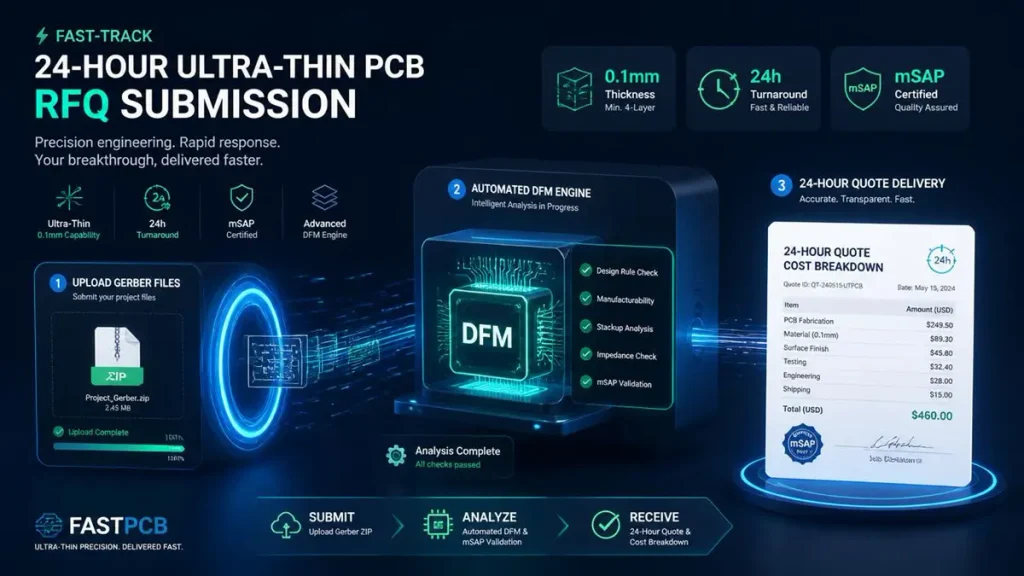
24-Hour Ultra-Thin PCB RFQ & DFM Automated Quoting Process
A well-designed quote request form is the final filter in the procurement decision chain. Hongda’s RFQ portal is optimized for buyers who have already completed the checklist above.
Form fields that reduce friction:
- Project name / company: Enables personalized quote headers and dedicated engineering assignment.
- Contact + time zone: Ensures our 24-hour response hits your inbox during business hours.
- File upload (multi-format): Gerber (.zip), BOM (.csv/.xlsx), assembly drawing (.pdf), stack-up notes.
- Quantity ladder: Separate fields for prototype, pre-production, and annual volume.
- Lead-time requirement: Standard (10–15 days), expedited (72 hours), or emergency (24–48 hours with material-in-stock confirmation).
- Special process checkboxes: Impedance control, blind/buried vias, via filling, high-Tg material, ceramic substrate, rigid-flex.
- Notes field: For thermal constraints, packaging requirements, or NDA references.
Primary CTA button: “Request Ultra-Thin PCB Quote”
Secondary CTA: “Download RFQ Checklist PDF” — for buyers still assembling documents; captures lead email for follow-up.
Frequently Asked Questions — What Procurement Buyers Google When Sourcing Ultra-Thin PCB Suppliers
What Documents Do I Need to Provide for an Accurate Ultra-Thin PCB Quotation?
At minimum, submit your Gerber RS-274X archive, NC drill files with plated/non-plated annotations, stack-up drawing with material specs, surface finish requirement, and a quantity ladder (prototype through mass production). For HDI or impedance-controlled boards, include the impedance table and via structure diagram. A complete package allows Hongda to deliver a locked quote in 24 hours without secondary revisions.
How Long Does It Take to Receive a Custom PCB Quote for Thin Boards?
Standard turnaround is 24 hours from complete file receipt. For expedited projects where material is in stock, Hongda’s engineering team can issue a preliminary ultra-thin PCB quotation within 4–8 hours. Delays typically occur only when stack-up data or impedance requirements are missing from the initial submission.
What Is the Minimum Thickness for a Reliable Ultra-Thin PCB Quote?
Hongda routinely manufactures 0.1 mm–0.4 mm finished thickness for 6- to 16-layer Any-Layer HDI boards. Achievable thickness depends on layer count, material selection (BT vs. modified FR-4), and whether the design uses coreless lamination. During DFM review, we validate whether your target thickness supports your required microvia density and copper weight.
Why Do Ultra-Thin PCB Quotes Vary So Much Between Suppliers?
Price variance usually traces back to three factors: (1) Process capability gaps—suppliers without mSAP or LDI will either decline complex jobs or quote conservatively; (2) Material sourcing—factories without allocated low-loss laminate inventory pad quotes against spot-market volatility; and (3) Test scope—some quotes exclude flying probe, AOI, or thermal shock validation. Hongda’s thin PCB quote includes all manufacturing, inspection, and reliability testing in a single transparent line item.
Can I Get a Low-Volume Custom PCB Quote for Prototypes Without Committing to Mass Production?
Yes. Hongda supports NPI volumes as low as 5 pieces with no minimum order penalty for standard materials. However, we recommend declaring your projected annual volume during RFQ submission. This allows our team to select panelization strategies and material formats that scale seamlessly from prototype to mass production, preventing re-qualification costs later.
Conclusion — Secure Your Ultra-Thin PCB Quotation with Manufacturing-Backed Confidence
The procurement decision chain for ultra-thin boards ends at one question: Can this supplier actually build what they are quoting? In 2026, the gap between quoting software and factory reality is widening—especially for AI hardware, smartphone modules, and wearable devices that push substrates below 0.4 mm.
Shenzhen Hongda Circuit Technology Co., Ltd. closes that gap by embedding 2026-grade equipment—LDI, mSAP, dual-beam laser drilling, 3D AI X-Ray, and vacuum lamination—directly into the ultra thin PCB quote workflow. The result is a 24-hour quotation that reflects real process capability, real material availability, and real DFM insight.
Ready to lock your pricing? Submit your Gerber files, stack-up, and quantity ladder through our RFQ portal at pcb@pcbkr.com and receive your production-ready custom PCB quote within 24 hours.
Internal Linking Recommendations for Content Cluster:
- Link to: Hongda HDI PCB technology page (anchor: “Any-Layer HDI manufacturing”)
- Link to: Hongda AI hardware PCB solutions (anchor: “224G PAM4 signal integrity”)
- Link to: Hongda high-frequency PCB materials guide (anchor: “Megtron 6/7 low-loss laminates”)
- Link to: Hongda DFM services page (anchor: “free DFM optimization review”)
Schema Markup Suggestion: Implement FAQPage schema for the five FAQs above, and Product schema with Offer for the CTA form to enhance AI-search visibility in Google SGE and Bing Copilot.
About Author
David Chen https://www.linkedin.com/in/pcbcoming
David Chen boasts an extensive professional background in PCBA manufacturing, PCBA testing, and PCBA optimization, with specialized expertise in high-precision PCBA fault analysis and rigorous PCBA reliability testing. The author has worked with high-layer-count server PCB fabrication, ultra-low-loss backplane stackups, and thermo-mechanical reliability optimization for AI infrastructure projects involving 112G and 224G PAM4 architectures. Skilled in complex circuit design and cutting-edge advanced PCB manufacturing processes, he delivers solutions that elevate product durability and performance across industrial applications. His technical articles focusing on PCBA manufacturing workflows and testing methodologies are widely cited by industry peers, research institutions, and technical platforms, solidifying his reputation as a recognized technical authority in the global circuit board manufacturing sector.