Via Fill PCB: Complete Engineering Guide for High-Reliability PCB Manufacturing
Introduction: Why Via Fill PCB Matters for Modern Electronics
For procurement engineers evaluating PCB suppliers, four questions dominate the sourcing decision:
- What is Via Fill PCB and how does it differ from conventional plated through-holes?
- Why is via filling necessary in high-reliability applications?
- When should you choose filled vias instead of standard plated vias?
- Which filling material delivers the best performance-to-cost ratio for your application?
The answer lies in the evolving demands of modern electronics. As data rates push beyond 112G PAM4 toward 224G and 448G in AI server backplanes, and as BGA pitches shrink below 0.4mm, traditional open vias create solder wicking risks, thermal bottlenecks, and signal integrity degradation. Via filling technology has transitioned from a niche capability to a baseline requirement for high-density interconnect (HDI) boards, AI accelerators, medical implants, and aerospace flight control systems.
This guide provides a systematic, engineering-level analysis of filled via PCB technology, manufacturing processes, IPC compliance frameworks, and material selection criteria—written from the perspective of a manufacturer with deep production experience in advanced via fill applications.
What Is Via Fill PCB? Definition and Core Concepts
Definition of Filled Via PCB Technology
A Via Fill PCB is a printed circuit board in which via holes are completely filled with conductive or non-conductive material, rather than merely plated with copper along the barrel walls. This structural difference fundamentally changes the board’s thermal, mechanical, and electrical characteristics.
The industry recognizes four distinct via configurations, and understanding their differences is critical for design-for-manufacturing (DFM):
| Via Type | Structure | Filling Material | Surface Finish | Primary Application |
|---|---|---|---|---|
| Filled Via | Hole completely filled | Resin, copper, or epoxy | Planarized flush with surface | High-reliability HDI, thermal management |
| Plugged Via | Hole partially filled (typically 60-80%) | Soldermask or resin | Not planarized; may be tented | Cost-sensitive designs, basic reliability |
| Capped Via | Filled via with additional copper cap over top | Resin + copper cap | Plated over cap | Via-in-pad (VIPPO), BGA breakout |
| Via in Pad | Via located directly under SMT pad | Copper or resin | Planarized and plated over | Fine-pitch BGA, 0.3-0.4mm pitch CSP |
Key Distinction: A filled via requires complete material penetration from top to bottom copper layers, verified by microsection analysis per IPC-TM-650. A plugged via only requires surface-level obstruction to prevent solder wicking during assembly, with no guarantee of internal void elimination.
Visual Comparison: Standard Via vs. Filled Via PCB
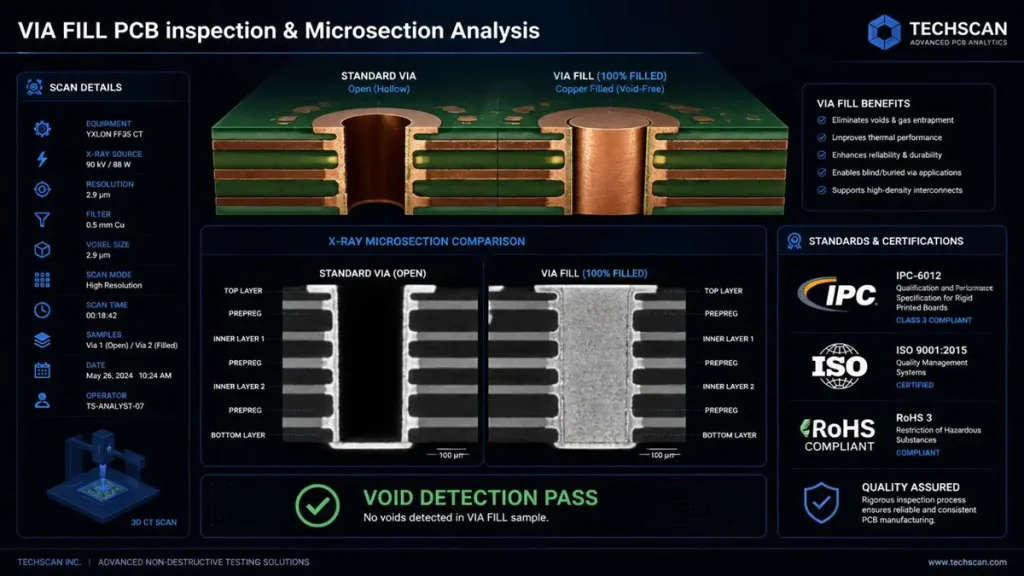
3D CT X-Ray Microsection Comparison Between Standard Open Via and Copper Filled Via (IPC Class 3 Compliant)
Standard Plated Via:
- Copper barrel thickness: 20-25μm typical
- Hollow center: Air or flux residue trapped
- Risk: Solder wicking during reflow, moisture ingress, thermal stress concentration
- Aspect ratio limitation: Up to 10:1 for reliable plating
Filled Via PCB:
- Complete material fill: Eliminates internal voids
- Planarized surface: Enables via-in-pad placement
- Enhanced thermal path: Continuous material from component pad to inner copper planes
- Improved mechanical strength: Reduces barrel cracking under thermal cycling
Why Is Via Filling Important? Engineering Benefits Explained
Via filling delivers measurable improvements across six critical performance domains. For procurement teams, these translate directly into field reliability metrics and total cost of ownership.
Better SMT Assembly and Prevent Solder Wicking
During lead-free reflow (peak temperatures 245-260°C), molten solder exhibits capillary action. In an open via located near a BGA pad, solder can wick down the barrel, starving the joint and creating open connections. IPC-A-610 Class 3 rejects any visible solder wicking exceeding 25% of pad diameter.
Filled Via Solution: Complete resin or copper fill blocks the capillary path. Shenzhen Hongda Circuit’s vacuum resin filling process achieves >99% fill rate, verified by X-ray inspection, eliminating solder wicking defects in 0.3mm pitch BGA assemblies.
Improve Heat Dissipation in High-Power Designs
Copper-filled vias create direct thermal pathways from component mounting pads to internal ground planes or backside heat sinks. The thermal conductivity of electroplated copper (~400 W/m·K) is approximately 1,600× higher than FR-4 substrate (~0.25 W/m·K).
Application Example: In AI server GPU modules dissipating 400-700W, arrays of copper-filled thermal vias under the processor reduce junction-to-case thermal resistance by 15-30% compared to standard vias with air cores. This enables sustained operation at full computational load without thermal throttling.
Increase Mechanical Strength and Board Reliability
Unfilled vias create stress concentration points during thermal cycling (-40°C to +125°C typical for automotive). The CTE mismatch between copper barrel (17 ppm/°C) and FR-4 substrate (14-16 ppm/°C Z-axis) generates shear stress at the barrel-wall interface.
Filled Via Advantage: Resin fill materials with CTE matched to copper (typically 30-50 ppm/°C below Tg, 150-200 ppm/°C above Tg) absorb expansion stress, reducing the incidence of barrel cracks and inner layer separation. IPC-6012 Class 3 requires 6× thermal cycles without degradation; filled vias routinely exceed 1,000 cycles in IST testing.
Better High-Speed Signal Integrity at 224G and Beyond
At 56GHz and 112G PAM4 data rates, via stubs become significant impedance discontinuities. A standard through-hole via in a 20-layer board may present a 15mm stub to a signal routed on layers 1-3, creating resonant reflections.
Filled Via Impact: While filling alone does not eliminate the stub, copper-filled vias enable backdrilling precision—the fill material provides a solid backstop for controlled-depth drilling, reducing stub length to <0.2mm. Combined with via-in-pad placement, this eliminates fanout stubs entirely, improving insertion loss by 0.5-1.2 dB at 28GHz.
Prevent Moisture Penetration and CAF Growth
Unfilled vias create vertical channels for moisture absorption. In humid environments (85°C/85% RH testing), moisture wicking along glass fibers can initiate conductive anodic filament (CAF) growth between adjacent vias, leading to insulation resistance failure.
Filled Via Protection: Epoxy and resin fills seal the via barrel, blocking moisture ingress paths. This is mandatory for medical implantable devices (ISO 13485) and automotive under-hood electronics (AEC-Q100 Grade 0).
Types of PCB Via Filling Technology: Material Selection Guide
The choice of via fill material determines electrical conductivity, thermal performance, CTE compatibility, and unit cost. Below is an engineering analysis of the four primary technologies, ranked by 2026 market adoption in high-reliability applications.
Non-Conductive Resin Filled Via (Most Common)
Characteristics:
- Material: Epoxy-based resin with silica filler (CTE 30-50 ppm/°C below Tg)
- Electrical conductivity: Insulating (<10⁻¹² S/m)
- Thermal conductivity: 0.3-0.8 W/m·K
- Process: Vacuum pressure impregnation → curing → planarization
Advantages:
- Lowest cost via fill option (adds 8-15% to bare board cost)
- Excellent CTE match to FR-4 substrate
- Compatible with all surface finishes (ENIG, OSP, Immersion Tin)
- Proven reliability in IPC-6012 Class 3 applications
Disadvantages:
- No electrical or thermal conduction through fill material
- Requires larger via diameter (>0.2mm) for reliable vacuum fill
- Not suitable for thermal via applications under high-power components
Best Applications:
General HDI boards, consumer electronics, industrial control, standard BGA breakout, cost-optimized designs where thermal management is handled through plane layers rather than vias.
Conductive Via Fill (Silver Epoxy)
Characteristics:
- Material: Silver flake-loaded epoxy (silver content 70-85% by weight)
- Electrical conductivity: 10⁴-10⁵ S/m (isotropic)
- Thermal conductivity: 2-5 W/m·K
- Process: Screen printing or needle dispensing → curing
Advantages:
- Provides electrical continuity between layers through the fill
- Moderate thermal improvement over resin
- Lower cost than copper filling for prototype quantities
Disadvantages:
- CTE mismatch: Silver epoxy CTE (50-80 ppm/°C) is significantly higher than copper, creating stress under thermal cycling
- Silver migration risk under bias humidity conditions
- Limited current-carrying capacity compared to solid copper
- IPC-4761 Type V (conductive fill) requires special qualification
Best Applications:
RF shielding vias, ESD protection networks, antenna grounding, low-current power distribution in non-critical consumer devices.
Copper Filled Via (AI Server and High-Performance Standard)
Characteristics:
- Material: Electroplated pure copper (99.9%+ purity)
- Electrical conductivity: 5.8×10⁷ S/m (equivalent to bulk copper)
- Thermal conductivity: ~400 W/m·K
- Process: Electroplating in specialized via fill bath → overplating → planarization
Advantages:
- Highest electrical and thermal conductivity of all fill options
- CTE matches barrel copper perfectly (17 ppm/°C)
- Enables via-in-pad with plated-over cap (VIPPO) for 0.3mm pitch
- Supports 224G/448G signal integrity requirements
- No material interface reliability concerns
Disadvantages:
- Highest cost (adds 25-40% to bare board cost)
- Requires specialized electroplating equipment with pulse-reverse capability
- Aspect ratio limitation: Typically <10:1 for void-free fill
- Longer plating time (4-8× standard plating)
Best Applications:
- AI Server PCBs: GPU baseboards, switch fabrics, NIC cards running 112G-448G
- Military/Aerospace: Flight control modules, radar systems, satellite communications
- Medical: Implantable neurostimulators, CT detector arrays
- Automotive: ADAS sensor fusion boards, EV battery management systems
Epoxy Filled Via (Cost-Optimized Alternative)
Characteristics:
- Material: Standard epoxy resin without conductive fillers
- Properties: Similar to non-conductive resin but with lower viscosity for better penetration
- Cost: Lowest among fill options (adds 5-10% to bare board cost)
Best Applications:
Single-layer fill in non-critical consumer electronics, LED lighting boards, basic industrial controllers where via sealing is required but thermal/electrical performance is not critical.
Via Plugging vs. Filled Via PCB: Critical Differences
| Parameter | Via Plugging | Filled Via |
|---|---|---|
| Fill percentage | 60-80% (partial) | >95% (complete) |
| Surface planarity | Not required | Required (±10μm) |
| Void allowance | Up to 25% | <5% per IPC-4761 |
| Solder wicking prevention | Partial | Complete |
| Via-in-pad capability | No | Yes |
| Thermal performance | Minimal improvement | Significant (copper fill) |
| Cost impact | Low (+3-5%) | Medium-High (+8-40%) |
| IPC standard | IPC-4761 Type I-II | IPC-4761 Type III-VII |
Procurement Recommendation: For BGA pitches below 0.5mm, high-reliability (Class 3), or thermal-critical designs, specify filled vias, not plugged vias. The cost delta is recovered through improved assembly yield and field reliability.
Via Fill PCB Manufacturing Process: Step-by-Step Engineering Analysis
The via fill manufacturing sequence is among the most process-critical operations in advanced PCB fabrication. Each step requires precise parameter control to achieve void-free fill and IPC-compliant reliability.
Step 1 — Precision Drilling and Laser Microvia Formation
Mechanical Drilling: Used for through-hole vias >0.2mm diameter. CNC drilling machines with high-speed spindles (180-200krpm) achieve positional accuracy ±25μm. For aspect ratios >8:1, controlled depth drilling with backdrill capability is required.
Laser Drilling (HDI Microvias): For 0.075-0.15mm microvias in AI server and smartphone PCBs, UV laser systems (355nm wavelength) provide ±10μm positional accuracy. CO₂ lasers (10.6μm) ablate dielectric material with natural stopping at copper layers, enabling blind via formation in sequential lamination builds.
Shenzhen Hongda Circuit Capability: Dual-head UV/CO₂ laser drilling systems process microvias down to 75μm diameter with automated vision alignment, supporting stacked microvia structures up to 3 layers deep per IPC-2226 guidelines.
Step 2 — Desmear and Plasma Cleaning
After drilling, resin smear and debris must be completely removed to ensure copper plating adhesion. The process sequence:
- Permanganate desmear: Oxidizes resin smear on hole walls
- Plasma cleaning: CF₄/O₂ plasma removes residual organic contamination and etches back epoxy to expose glass fibers
- Conditioner: Electroless copper deposition preparation
Critical Control Parameter: Plasma etch rate must be maintained at 0.5-1.0μm/min to avoid over-etching thin dielectric layers in high-layer-count builds.
Step 3 — Electroless Copper Deposition
A thin (0.5-1.0μm) electroless copper layer is deposited to provide conductivity for subsequent electrolytic plating. The bath uses formaldehyde-based chemistry with palladium catalyst activation.
Quality Check: Backlight testing verifies continuous copper coverage in high-aspect-ratio holes. Any discontinuity results in plating voids after fill.
Step 4 — Copper Plating (For Copper-Filled Vias)
Standard DC plating cannot achieve void-free via fill due to non-uniform current distribution. Copper-filled vias require:
- Pulse-reverse plating: Alternating forward/reverse current pulses (10-100Hz) with optimized duty cycle
- High-throw chemistry: Organic additives (brighteners, carriers, levelers) specifically formulated for via fill
- Current density control: 1.5-3.0 A/dm² with real-time bath analysis
Fill Quality Metric: Cross-section analysis must show <5% void area per IPC-4761. Shenzhen Hongda Circuit achieves <3% voids in 10:1 aspect ratio vias through optimized pulse parameters.
Step 5 — Via Filling (Resin or Copper)
Resin Filling Process:
- Vacuum deaeration of resin to remove dissolved air
- Panel placement in vacuum chamber (pressure <10 mbar)
- Resin injection under pressure (3-5 bar)
- Curing: 150°C for 60-90 minutes (thermal profile per resin TDS)
- Cooling rate control: <3°C/min to prevent CTE-induced cracking
Copper Filling Process:
- Panel pre-treatment: Acid clean → micro-etch → activator
- Via fill electroplating: 8-16 hours in dedicated fill line
- Overplating: Additional 20-30μm copper for planarization allowance
- Surface grinding to remove excess copper
Step 6 — Planarization Grinding
Filled vias must be planarized to ±10μm coplanarity before surface finish application. Belt grinding with diamond abrasives (800-1200 grit) removes overfill, followed by chemical mechanical polishing (CMP) for final surface preparation.
Yield Impact: Grinding depth control is critical—over-grinding exposes voids; under-grinding leaves copper bumps that interfere with solder mask application.
Step 7 — Surface Finish and Final Inspection
Compatible Surface Finishes for Filled Vias:
- ENIG (Electroless Nickel Immersion Gold): Most common; 3-5μm nickel, 0.05-0.1μm gold
- ENEPIG: Enhanced wire bondability for RF modules
- Immersion Silver: Cost-effective for high-volume consumer
- OSP: Limited compatibility; requires careful process control
Inspection Protocol:
- AOI (Automated Optical Inspection): 100% surface coverage for plating defects
- X-ray Inspection: Void detection in filled vias; IPC-4761 requires <5% voids in cross-section
- Microsection Analysis: Destructive testing per IPC-TM-650 Method 2.1.1 for via wall integrity, copper thickness, and fill percentage
- Electrical Test: Flying probe or bed-of-nails for opens/shorts
PCB Via Filling Materials Comparison: Engineering Data Table
| Property | Non-Conductive Resin | Copper Electroplated | Silver Epoxy | Standard Epoxy |
|---|---|---|---|---|
| Electrical Conductivity | Insulating | 5.8×10⁷ S/m | 1×10⁵ S/m | Insulating |
| Thermal Conductivity | 0.3-0.8 W/m·K | ~400 W/m·K | 2-5 W/m·K | 0.2-0.4 W/m·K |
| CTE (Below Tg) | 30-50 ppm/°C | 17 ppm/°C | 50-80 ppm/°C | 40-60 ppm/°C |
| Reliability (Thermal Cycles) | Excellent (>1000×) | Excellent (>1000×) | Moderate (500×) | Good (800×) |
| Relative Cost | Low (1.0×) | High (3.5×) | Medium (2.0×) | Lowest (0.7×) |
| IPC Compliance | IPC-4761 Type III | IPC-4761 Type VII | IPC-4761 Type V | IPC-4761 Type I |
| Best Application | General HDI, BGA | AI servers, thermal vias | RF shielding, ESD | Cost-sensitive consumer |
Filled Via vs Plugged Via vs Tented Via vs Open Via: Complete Comparison
| Comparison Factor | Filled Via PCB | Plugged Via | Tented Via | Open Via |
|---|---|---|---|---|
| Manufacturing Complexity | High (vacuum fill + grind) | Medium (mask/screen) | Low (soldermask only) | Lowest (standard process) |
| Cost Impact | +15-40% | +3-8% | +1-3% | Baseline |
| Reliability (IPC Class) | Class 2 & 3 | Class 2 | Class 1-2 | Class 1-2 |
| Signal Integrity | Excellent (stub control) | Good | Poor (stub present) | Poor |
| Thermal Performance | Excellent (copper fill) | Minimal | Minimal | Minimal |
| Assembly Compatibility | All SMT processes | Limited fine-pitch | Standard | Standard |
| IPC Standard Reference | IPC-4761 Type III-VII | IPC-4761 Type I-II | IPC-4761 Type VI | N/A |
| Typical Applications | AI servers, medical, aerospace | Industrial, automotive | Consumer, low-density | Prototypes, non-critical |
IPC Standards for Via Fill PCB: Compliance Framework
IPC standards govern every aspect of via fill quality, from design rules to acceptance criteria. Procurement engineers should verify supplier compliance against these specifications.
IPC-4761 — Via Protection and Filling Guidelines
IPC-4761 defines seven via protection types, with Types III-VII specifically addressing filled vias:
- Type III (Filled Via, Non-Conductive): Via filled with non-conductive material; no surface cap
- Type IV (Filled Via, Non-Conductive + Capped): Filled and overplated with copper
- Type V (Filled Via, Conductive): Silver or carbon-filled epoxy
- Type VI (Filled Via, Conductive + Capped): Conductive fill with copper cap
- Type VII (Copper Filled Via): Electroplated copper fill, the highest reliability category
IPC-6012 — Qualification and Performance Specification
IPC-6012E (2025 revision) specifies acceptance criteria for rigid boards:
- Class 2 (Dedicated Service): Acceptable for industrial, automotive, non-critical military
- Class 3 (High Reliability): Required for life support, flight control, missile systems
- Class 3/A (Space): Additional thermal vacuum outgassing requirements
Key Requirements for Filled Vias:
- Thermal stress testing: 6× cycles at 288°C for 10 seconds (Class 3)
- Microsection: Minimum 20μm copper barrel; <5% voids in fill
- Solderability: Wetting balance test per IPC-J-STD-003
IPC-2221 / IPC-2226 — Design Standards
- IPC-2221: Generic standard for printed board design; specifies annular ring, pad size, and clearance requirements
- IPC-2226: Sectional design standard for HDI boards; defines microvia structures, stacked via rules, and sequential lamination guidelines
Critical Design Rule: For microvias in Type III HDI (stacked), IPC-2226 limits stacking to 2-3 layers with copper-filled and planarized structures to prevent electromigration failures.
MIL-STD-55110 / MIL-PRF-31032
Military applications require additional qualification:
- MIL-PRF-31032: Performance specification for printed circuit boards
- QPL Listing: Qualified Products List certification required for defense contractors
- ITAR Compliance: Required for boards used in munitions, satellites, and encryption hardware
Via in Pad Filled and Capped PCB (VIPPO) Technology
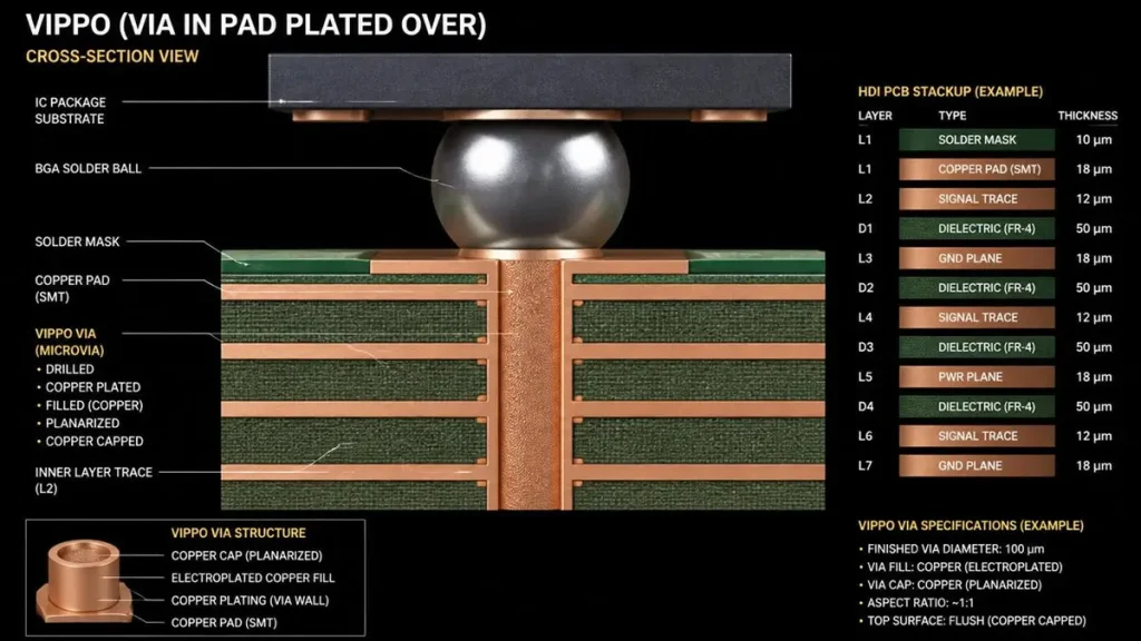
Detailed Engineering Cross-Section of a VIPPO (Via in Pad Plated Over) Structure with BGA Solder Ball & HDI Stackup
VIPPO (Via in Pad Plated Over) Explained
Via in Pad Plated Over (VIPPO) is the premier application of copper-filled via technology. The via is drilled directly through the component mounting pad, filled with copper, planarized, and overplated with the surface finish (ENIG/ENEPIG).
Why BGAs Require VIPPO:
Modern CPUs, GPUs, FPGAs, and AI accelerators use BGA pitches of 0.3-0.4mm with thousands of I/Os. Traditional “dog bone” fanout routing requires escape traces that consume precious layer real estate. At 0.3mm pitch, there is insufficient space between pads for traces and vias.
VIPPO Solution:
- Via placed directly under BGA pad
- No fanout traces needed
- Enables 4-6 layer reduction in escape routing
- Supports 0.3mm pitch CSP and WLCSP packages
Applications Requiring VIPPO:
- CPU/GPU Baseboards: Intel Xeon, AMD EPYC, NVIDIA H100/H200 modules
- FPGA Boards: Xilinx Versal, Intel Agilex for 5G base stations
- ASIC Accelerators: Google TPU, custom AI training chips
- AI Modules: NVIDIA Jetson, Qualcomm RB3 for edge AI
Filled Microvias in HDI PCB: Stacked and Staggered Structures
Microvia Definitions and Laser Drilling
Per IPC-2226, a microvia is defined as:
- Diameter ≤0.15mm (150μm)
- Depth ≤0.25mm
- Aspect ratio ≤1:1
Laser Drilling Technologies (2026):
- CO₂ Lasers (10.6μm): Ablate dielectric with natural copper stop; ideal for blind vias in build-up layers
- UV Lasers (355nm): Penetrate copper and dielectric; enable 50-75μm vias for ultra-HDI
- Picosecond Lasers: Minimize heat-affected zones (HAZ) in high-Tg materials; enable <50μm vias
Stacked vs. Staggered Microvia Architecture
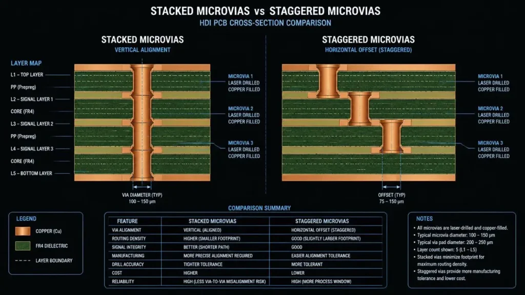
Engineering Cross-Section Comparison of Stacked Microvias vs. Staggered Microvias in High-Density HDI PCBs
| Structure | Description | Reliability | Layer Density | Manufacturing Cost |
|---|---|---|---|---|
| Stacked Microvia | Vias aligned vertically; direct layer-to-layer connection | Moderate (stress concentration) | Highest | Medium |
| Staggered Microvia | Vias offset between layers; no vertical alignment | Highest (stress distributed) | High | Medium-High |
| Skip-Via | Microvia connects non-adjacent layers | High | Medium | Low |
IPC-2226 Stacking Rule: Maximum 2 stacked microvias in standard builds; 3 allowed only with copper-filled and planarized structures in sequential lamination.
Shenzhen Hongda Circuit HDI Capability:
- Laser microvias down to 75μm
- Stacked microvia structures up to 3 layers (Type III HDI)
- Sequential lamination up to 6 build-up cycles
- Any-layer HDI (Type VI) for smartphone and wearable applications
Thermal Performance of Via Fill PCB: Quantitative Analysis
Heat Transfer Mechanisms in Filled Vias
The thermal resistance (Rth) of a via is calculated as:
Rth = L / (k × A)
Where:
- L = via length (board thickness)
- k = thermal conductivity of fill material
- A = cross-sectional area of via
Comparison for 0.3mm diameter via through 1.6mm board:
| Fill Material | k (W/m·K) | Rth (°C/W) | Relative Performance |
|---|---|---|---|
| Air (open via) | 0.026 | 872 | Baseline (1×) |
| Non-conductive resin | 0.5 | 45 | 19× improvement |
| Silver epoxy | 3.0 | 7.5 | 116× improvement |
| Copper (electroplated) | 400 | 0.056 | 15,571× improvement |
Practical Impact: A copper-filled thermal via array (20 vias, 0.3mm diameter) under a 100W GPU reduces thermal resistance from junction to heatsink by approximately 0.5°C/W, enabling 15-20W additional power dissipation within the same thermal envelope.
Thermal Simulation and IR Validation
Shenzhen Hongda Circuit provides thermal simulation services using ANSYS Icepak and Flotherm XT. IR thermography validation confirms simulation accuracy within ±3°C. For AI server customers, this enables pre-production thermal optimization, eliminating costly respins.
Signal Integrity Benefits of Filled Via PCB at 224G PAM4
High-Speed Design Challenges
Modern data center interconnects operate at:
- 56G NRZ: 28GHz Nyquist frequency
- 112G PAM4: 28GHz with 4-level signaling
- 224G PAM4: 56GHz (emerging 2026-2027)
- 448G PAM4: 112GHz (research phase)
At these frequencies, via stubs behave as quarter-wave resonators, creating deep nulls in insertion loss.
Filled Via Impact on Eye Diagram and Insertion Loss
Backdrill Enhancement: Copper-filled vias provide a solid backstop for controlled-depth backdrilling. The fill material prevents drill bit “wandering” and copper smear, enabling stub reduction to <0.2mm.
Measured Improvements (Shenzhen Hongda Circuit Test Vehicle, 20-layer, 1.6mm):
| Via Configuration | Stub Length | Insertion Loss @28GHz | Eye Height @112G PAM4 |
|---|---|---|---|
| Standard through-hole | 15.0mm | -12.5 dB | 85 mV |
| Backdrilled open via | 0.5mm | -8.2 dB | 142 mV |
| Copper-filled + backdrill | 0.2mm | -6.8 dB | 168 mV |
| VIPPO (no stub) | 0mm | -5.5 dB | 195 mV |
Conclusion: VIPPO with copper-filled vias provides 2.3× eye height improvement over standard vias, directly translating to bit error rate (BER) reduction from 10⁻⁵ to <10⁻¹².
Reliability Testing for Filled Via PCB
Accelerated Life Testing Protocols
| Test | Standard | Conditions | Acceptance | Purpose |
|---|---|---|---|---|
| Thermal Cycling | IPC-TM-650 2.6.7 | -65°C to +150°C, 1000 cycles | No barrel cracks, <10% resistance change | CTE mismatch validation |
| IST (Interconnect Stress Test) | IPC-TM-650 2.6.26 | 25°C to 150°C, 6 cycles/min | >300 cycles to failure | Plating integrity |
| CAF Resistance | IPC-TM-650 2.6.25 | 85°C/85%RH, 1000V bias, 1000hrs | >10⁸ Ω insulation | Moisture/ion migration |
| SIR (Surface Insulation Resistance) | IPC-TM-650 2.6.3.3 | 85°C/85%RH, 50V, 168hrs | >10⁸ Ω | Contamination assessment |
| HAST (Highly Accelerated Stress Test) | JESD22-A110 | 130°C/85%RH, 33.3psia, 96hrs | No delamination, voids | Humidity acceleration |
| HALT/HASS | IEC 60068-2-6 | Vibration + thermal combined | No structural failure | Field stress simulation |
Microsection and Cross-Section Analysis
Destructive microsectioning per IPC-TM-650 Method 2.1.1 is the definitive quality verification for filled vias. Key measurements:
- Copper barrel thickness: Minimum 20μm (Class 3), 25μm preferred for high-aspect-ratio
- Fill percentage: >95% (Type III), >99% (Type VII copper fill)
- Void size: Maximum individual void <5% of via diameter; total voids <5% of fill volume
- Copper cap thickness: 20-30μm for VIPPO applications
- Wall roughness: <25μm Ra for high-speed signal vias
Design Guidelines for Via Fill PCB
Critical Dimensional Parameters
| Parameter | Recommended Value | Notes |
|---|---|---|
| Via Diameter | 0.15-0.30mm (microvia); 0.20-0.50mm (through-hole) | Smaller vias harder to fill completely |
| Aspect Ratio | <10:1 for copper fill; <12:1 for resin fill | Higher ratios risk voids |
| Annular Ring | ≥50μm (Class 2); ≥25μm (Class 3) | Captures registration tolerance |
| Pad Size (VIPPO) | Via diameter + 0.10mm minimum | Ensures cap integrity |
| Capture Pad | 0.20-0.35mm oversize for microvias | IPC-2226 recommendation |
| Clearance to Trace | ≥0.075mm (3 mil) for HDI | Prevents CAF initiation |
| Copper Thickness | 1oz (35μm) base; 2-4oz for power | Heavier copper improves thermal |
| Stackup Symmetry | Balanced copper distribution | Prevents warpage |
DFM and DFT Considerations
Design for Manufacturing (DFM):
- Specify laser-drillable materials (low-Tg, non-glass-heavy) for microvias
- Limit stacked microvias to 2-3 per IPC-2226
- Maintain 50-100μm dielectric between microvia layers for 0.75:1 aspect ratio
- Use teardrop shapes at trace-to-pad junctions to reduce stress
Design for Test (DFT):
- Place test pads on grid (100 mil standard) for flying probe access
- Avoid filled vias as test points (surface planarity affects probe contact)
- Provide isolation resistors for boundary scan chains
- Include Kelvin sense lines for high-current path verification
Common Manufacturing Defects in Via Fill PCB and Prevention
| Defect | Description | Root Cause | Prevention | Repairability |
|---|---|---|---|---|
| Void | Air pocket in fill material | Outgassing, insufficient vacuum | Vacuum <10mbar, slow curing | Not repairable; scrap panel |
| Sink | Depression in fill surface | Excessive shrinkage | CTE-matched resin, controlled cure | Limited; may accept if <10μm |
| Crack | Fracture in fill or barrel | CTE mismatch, thermal shock | Material selection, ramp rate control | Not repairable |
| Delamination | Separation at layer interface | Moisture, inadequate prep | Plasma desmear, bake-out | Not repairable |
| Overfill | Excess material above surface | Excessive resin volume | Precise volume control, grinding | Correctable by grinding |
| Underfill | Incomplete fill, exposed barrel | Insufficient resin, high aspect ratio | Vacuum optimization, pre-heating | Not repairable |
| Air Bubble | Spherical void near surface | Trapped air during injection | Vacuum impregnation, slow fill rate | Not repairable |
| Misregistration | Via off-center from pad | Drilling accuracy, material shift | Vision alignment, pinning | Not repairable |
| Copper Crack | Fracture in cap plating | Excessive grinding stress | Optimized grind parameters | Not repairable |
Yield Impact: Resin-filled vias typically achieve 92-96% first-pass yield; copper-filled vias 85-92% due to plating complexity. Shenzhen Hongda Circuit’s statistical process control (SPC) monitoring reduces defect PPM to <500 for high-volume production.
Applications of Via Fill PCB by Industry
AI Servers and Data Center Infrastructure
Technology Drivers:
224G/448G PAM4, PCIe 6.0/7.0, CXL 3.0
PCB Requirements:
- 20-32 layer HDI with any-layer microvia capability
- Copper-filled microvias for thermal management under 400-700W GPUs
- VIPPO for 0.3mm pitch BGA on switch ASICs and NIC controllers
- Low-loss materials (Megtron 6/7, EM-890K) with Df <0.002
Shenzhen Hongda Circuit AI Server Capability: Copper-filled microvias, sequential lamination up to 32 layers, impedance control ±5%, and 224G test vehicle validation.
Medical Equipment and Implantable Devices
Applications:
CT detector arrays, MRI RF coils, ultrasound probes, pacemakers, neurostimulators
Requirements:
ISO 13485, biocompatibility, hermetic sealing, 15+ year reliability
Via Fill Solution:
Non-conductive resin-filled microvias with ENIG finish; copper-filled thermal vias for high-power imaging electronics.
Aerospace and Satellite Systems
Applications:
Flight control computers, satellite communication payloads, radar T/R modules
Requirements:
MIL-PRF-31032, QPL listing, radiation tolerance, -55°C to +125°C operation
Via Fill Solution:
Copper-filled vias with polyimide substrate for outgassing compliance; stacked microvias with 100% fill for signal integrity in phased array antennas.
Military and Defense Electronics
Applications:
Missile guidance, secure communications, avionics displays
Requirements:
ITAR compliance, IPC Class 3/A, tamper resistance
Via Fill Solution:
Type VII copper-filled vias with conformal coating; buried filled vias for anti-tamper layer protection.
Automotive Electronics and ADAS
Applications:
ADAS sensor fusion, EV battery management, OBC (on-board charger), 77GHz radar
Requirements:
AEC-Q100/200, IATF 16949, 0ppm field failure target
Via Fill Solution:
Resin-filled vias for BGA processors; copper-filled thermal vias under IGBT modules; VIPPO for 0.4mm pitch ECU connectors.
Industrial Control and Power Electronics
Applications:
Servo drives, PLCs, IGBT modules, power supplies
Requirements:
High voltage isolation (up to 10kV), heavy copper (4-10oz), thermal cycling
Via Fill Solution:
Copper-filled vias in heavy copper boards; non-conductive fill for high-voltage isolation barriers.
How to Choose a Reliable Via Fill PCB Manufacturer
Procurement engineers should evaluate suppliers against these eight criteria:
- Equipment Portfolio: UV/CO₂ laser drilling, vacuum resin filling lines, pulse-reverse copper plating, automated grinding/CMP
- IPC Certification: Active IPC membership, Class 3 manufacturing qualification, IPC-6012 lab certification
- Quality System Certifications: ISO 9001, ISO 13485 (medical), IATF 16949 (automotive), AS9100 (aerospace)
- Inspection Capability: X-ray (2D/3D CT), AOI, flying probe, microsection lab, impedance testing
- HDI Experience: Proven track record with Type III-VI HDI, any-layer builds, sequential lamination
- Copper Filling Capability: Dedicated electroplating lines for via fill, <5% void achievement, VIPPO production
- Engineering Support: DFM review, stackup design, signal integrity simulation, thermal modeling
- On-Time Delivery: >95% OTD performance, buffer stock for long-lead materials
Why Choose Shenzhen Hongda Circuit Technology Co., Ltd. for Via Fill PCB
Shenzhen Hongda Circuit Technology Co., Ltd. has invested strategically in advanced via fill capabilities to serve the most demanding applications in AI, medical, aerospace, and automotive electronics. Our manufacturing ecosystem is built on three pillars: advanced equipment, rigorous quality systems, and deep engineering expertise.
Advanced Manufacturing Capabilities
- Laser Drilling: Dual-head UV (355nm) and CO₂ laser systems for microvias down to 75μm with ±10μm positional accuracy
- HDI Manufacturing: Type III-VI HDI with up to 6 sequential lamination cycles; any-layer routing capability
- Copper-Filled Microvias: Dedicated pulse-reverse electroplating lines achieving <3% voids in 10:1 aspect ratio vias
- Resin-Filled Vias: Vacuum pressure impregnation systems with automated volume control and thermal profiling
- Sequential Lamination: 20-32 layer builds with controlled impedance on all signal layers
- Via-in-Pad Processing (VIPPO): Full copper fill, planarization, and ENIG/ENEPIG surface finish for 0.3mm pitch BGA
- High-Layer-Count PCB Production: Up to 40 layers with heavy copper (up to 10oz) and mixed press capabilities
Advanced Equipment and Process Technology
| Equipment Category | Technology | Capability |
|---|---|---|
| UV Laser Drilling | 355nm picosecond laser | 75μm microvias, ±10μm accuracy |
| CO₂ Laser Drilling | Q-switched, dual-head | 100-150μm blind vias, natural copper stop |
| Laser Direct Imaging (LDI) | UV LDI with autofocus | 20μm line/space, ±8μm registration |
| Vacuum Resin Filling | Pressure/vacuum impregnation | >99% fill rate, void <3% |
| Copper Via Filling Lines | Pulse-reverse plating | 10:1 aspect ratio, <3% voids |
| Automated Optical Inspection | 3D AOI with AI defect classification | 100% surface coverage |
| Flying Probe Test | 4-head flying probe | 10,000+ test points, 0.1Ω resolution |
| X-Ray Inspection | 3D CT X-ray | Internal void detection, BGA analysis |
| Automatic Optical Shaping | Laser-based copper balancing | Warpage control <0.5% |
| High-Precision CNC Drilling | 200krpm spindle, linear motor | ±25μm, 0.1mm mechanical vias |
| Plasma Desmear | CF₄/O₂ plasma | Uniform hole conditioning, no glass protrusion |
| Impedance Test Systems | TDR with 40GHz bandwidth | ±5% impedance control |
| Microsection Laboratory | Grinding/polishing + optical measurement | IPC-TM-650 compliant analysis |
Quality Certifications and Compliance
- ISO 9001:2015 — Quality Management System
- ISO 13485:2016 — Medical Device Quality Management
- IATF 16949:2016 — Automotive Quality Management
- IPC Class 2 & Class 3 Manufacturing — Rigid PCB qualification
- RoHS & REACH Compliance — Environmental substance control
- MIL-PRF-31032 Capability — Defense and aerospace qualification path
Frequently Asked Questions (FAQ) for Procurement Engineers
What is the difference between via fill and via plug in PCB manufacturing?
Via fill completely fills the via hole with resin, copper, or epoxy, achieving >95% fill volume with planarized surface finish. Via plug only partially fills the hole (typically 60-80%) with soldermask or resin to prevent solder wicking, without surface planarity requirements. For BGA pitches below 0.5mm or IPC Class 3 reliability, specify filled vias, not plugged vias.
Why do copper-filled vias cost more than resin-filled vias, and when are they worth the premium?
Copper-filled vias require dedicated pulse-reverse electroplating lines with 4-8× longer plating time and specialized chemistry. The cost premium (25-40% vs. resin fill) is justified when: (a) thermal management is critical (GPU, power modules), (b) via-in-pad is required for 0.3-0.4mm pitch BGA, (c) signal integrity at 112G+ demands stub elimination, or (d) the application requires MIL/aerospace reliability.
What aspect ratio is achievable for reliable copper-filled vias, and how does it affect my design?
Shenzhen Hongda Circuit achieves reliable copper fill in vias with aspect ratios up to 10:1 (depth:diameter). For a 1.6mm board, this means minimum via diameter of 0.16mm. For 3.2mm boards, minimum 0.32mm. Exceeding 10:1 risks plating voids and requires resin fill or alternative routing. Design early with your manufacturer’s capability matrix.
How are filled vias inspected, and what acceptance criteria should I specify?
Filled vias require multi-modal inspection: (1) X-ray for void detection (<5% per IPC-4761), (2) Microsection for copper thickness and fill percentage (destructive, sample-based), (3) AOI for surface planarity and cap integrity, (4) Electrical test for continuity. Specify IPC-6012 Class 3 with microsection report for high-reliability builds.
Which surface finishes are compatible with filled via PCBs, and which is best for my application?
ENIG (Electroless Nickel Immersion Gold) is the most compatible and widely used finish for filled vias, providing excellent solderability and shelf life. ENEPIG adds a palladium layer for enhanced wire bondability (RF modules). Immersion Silver offers cost savings for high-volume consumer but has shorter shelf life. OSP is generally not recommended for VIPPO due to planarity sensitivity. For AI servers and medical devices, specify ENIG or ENEPIG.
Strategic Sourcing for Via Fill PCB Technology
Via fill PCB technology has evolved from a specialized capability to a foundational requirement for high-reliability electronics. The transition from open vias to filled vias—whether resin-filled for cost-optimized HDI or copper-filled for AI server thermal management—represents a strategic design decision that impacts signal integrity, thermal performance, assembly yield, and long-term field reliability.
For procurement engineers, the key selection criteria are: (1) material match to application requirements, (2) manufacturer capability in the specific fill technology, (3) IPC compliance level appropriate to end-use environment, and (4) total cost of ownership including yield improvement and field failure reduction.
Shenzhen Hongda Circuit Technology Co., Ltd. offers comprehensive via fill capabilities—from 75μm laser-drilled microvias to 10:1 aspect ratio copper-filled through-holes—backed by ISO 13485, IATF 16949, and IPC Class 3 manufacturing systems. Our engineering team provides DFM review, stackup optimization, and thermal simulation to ensure your design achieves manufacturability and performance targets on the first build.
For technical consultations or quotation requests for Via Fill PCB projects, contact Shenzhen Hongda Circuit Technology Co., Ltd. Engineering Team.
About Author
David Chen https://www.linkedin.com/in/pcbcoming
David Chen boasts an extensive professional background in PCBA manufacturing, PCBA testing, and PCBA optimization, with specialized expertise in high-precision PCBA fault analysis and rigorous PCBA reliability testing. The author has worked with high-layer-count server PCB fabrication, ultra-low-loss backplane stackups, and thermo-mechanical reliability optimization for AI infrastructure projects involving 112G and 224G PAM4 architectures. Skilled in complex circuit design and cutting-edge advanced PCB manufacturing processes, he delivers solutions that elevate product durability and performance across industrial applications. His technical articles focusing on PCBA manufacturing workflows and testing methodologies are widely cited by industry peers, research institutions, and technical platforms, solidifying his reputation as a recognized technical authority in the global circuit board manufacturing sector.