Blind & Buried Via PCB: Complete Manufacturing, Design, Materials & Cost Guide
Table of Contents
- What Is a Blind & Buried Via PCB?
- How Blind Vias Work vs. How Buried Vias Work
- Blind Via vs Buried Via vs Through Hole: Technical Comparison
- Blind & Buried Via PCB Structure Types
- Advanced Manufacturing Process for Blind & Buried Via PCBs
- Material Selection for High-Performance Blind & Buried Via PCBs
- Blind & Buried Via PCB Stackup Design Guide
- Critical Design Rules for Blind & Buried Via PCBs
- Signal Integrity Optimization in Blind & Buried Via PCBs
- Reliability Testing & IPC Standards for Blind & Buried Via PCBs
- Cost Analysis: Blind Via PCB vs Buried Via PCB Manufacturing
- Industry Applications of Blind & Buried Via PCBs
- Why Choose Shenzhen Hongda Circuit Technology Co., Ltd.
- Frequently Asked Questions (FAQ)
- Core FAQs for Procurement Searching Blind/Buried Via PCB Suppliers on Google
What Is a Blind & Buried Via PCB? Definition, Structure & Core Concepts
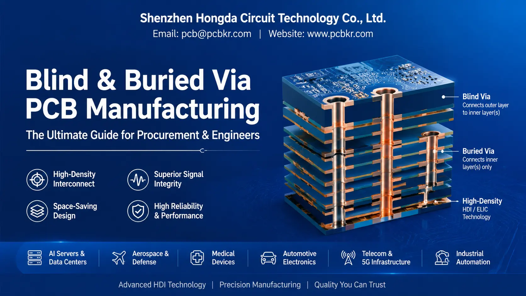
A Blind & Buried Via PCB is a type of high-density interconnect (HDI) printed circuit board that utilizes specialized via structures—blind vias and buried vias—to establish electrical connections between specific layers without penetrating the entire board thickness. Unlike conventional through-hole vias that traverse all layers from top to bottom, these advanced via configurations enable designers to optimize routing density, improve signal integrity, and reduce overall board dimensions.
Definition of a Blind Via PCB
A blind via connects an outer layer to inner layers without extending through the board. For step-by-step layer transition rules, explore our complete blind via PCB design and manufacturing guide. The term “blind” refers to the fact that the via is visible from only one side of the board. In modern HDI blind via PCB designs, these vias are typically created using UV laser drilling technology, achieving diameters as small as 75–150 μm with exceptional positional accuracy.
Blind vias serve as the primary mechanism for escaping high-pin-count components such as fine-pitch BGAs (Ball Grid Arrays) and CSPs (Chip Scale Packages). By terminating at intermediate layers rather than passing through the entire stackup, blind vias eliminate unnecessary via stubs that would otherwise degrade high-speed signal performance.
Definition of a Buried Via PCB
A buried via is a plated interconnect that exists entirely within the internal layers of a multilayer PCB, with no exposure to either the top or bottom surface. These vias are fabricated during the inner-layer processing stage and are subsequently laminated between core layers, rendering them invisible from the exterior of the finished board.
Buried via PCB technology is particularly valuable in high-layer-count designs (12L, 16L, 20L+) where internal routing channels must be established without consuming precious surface real estate. Because buried vias do not interfere with component placement or solder mask application on outer layers, they enable more aggressive component density and cleaner surface finishes.
How Blind Vias Work: The Electrical & Mechanical Principle
Blind vias function as controlled impedance transitions between surface-mounted components and internal signal layers. When a high-speed signal exits a BGA pad on the top layer, it enters the blind via barrel, which acts as a short vertical transmission line segment. The via barrel is electroplated with copper to a thickness of 20–25 μm, ensuring low-resistance current flow and adequate mechanical strength.
The critical performance parameter for blind vias is the aspect ratio—the ratio of via depth to drilled diameter. For reliable copper plating, aspect ratios should ideally not exceed 0.8:1 to 1:1. For example, a 100 μm diameter blind via drilled to a depth of 80 μm achieves an optimal 0.8:1 aspect ratio, allowing the plating chemistry to circulate effectively to the via bottom and deposit uniform copper without voids.
In laser-drilled blind via applications, the drilling process uses a combination of CO₂ and UV lasers. The CO₂ laser ablates the dielectric material, while the UV laser precisely removes the copper foil at the via landing pad. This dual-laser approach achieves registration accuracy within ±25 μm, which is essential for connecting to capture pads as small as 200 μm in diameter.
How Buried Vias Work: Internal Interconnection Architecture
Buried vias operate as dedicated routing highways within the core of the PCB. During fabrication, the inner layers containing buried vias are drilled, plated, and etched as sub-assemblies before being laminated into the final multilayer structure. This sequential construction means that buried vias are permanently encapsulated within the board and cannot be accessed after lamination.
The manufacturing of buried vias typically employs mechanical drilling with high-precision CNC drill machines. Because these vias do not require the extreme miniaturization of microvias, mechanical drilling offers cost advantages while maintaining the positional accuracy needed for multilayer registration. Buried via diameters commonly range from 200 μm to 300 μm, with aspect ratios up to 10:1 achievable in advanced facilities.
A key advantage of buried vias is their complete isolation from the board’s external environment. This encapsulation provides superior protection against moisture ingress, ionic contamination, and mechanical stress during assembly operations. For applications requiring IPC Class 3 reliability—such as aerospace, military, and medical devices—buried vias contribute to long-term interconnect stability by eliminating surface-exposed features that could become failure initiation points.
Blind Via vs Buried Via vs Through Hole: Technical Comparison
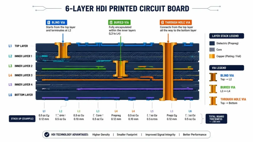
6-Layer HDI PCB Via Architecture: Blind, Buried & Through-Hole Comparison
Selecting the appropriate via type is one of the most consequential decisions in multilayer PCB design. For a direct feature-by-feature evaluation, review our detailed blind via vs buried via PCB comparison to analyze trade-offs in density, routability, and overall cost.
| Parameter | Blind Via | Buried Via | Through Hole Via |
|---|---|---|---|
| Definition | Connects outer layer to adjacent inner layer(s); visible from one side only | Connects internal layers only; completely hidden within board | Connects top to bottom layer; penetrates entire board |
| Visibility | Visible from one external surface | Invisible from all external surfaces | Visible from both top and bottom |
| Drilling Method | UV/CO₂ laser drilling (primary); mechanical (limited) | Mechanical drilling (primary); laser (special cases) | Mechanical drilling |
| Typical Diameter | 75–150 μm (laser); 200–300 μm (mechanical) | 200–350 μm | 250–500 μm |
| Aspect Ratio Limit | ≤0.8:1 (laser); ≤1:1 (mechanical) | ≤10:1 | ≤12:1 (standard); ≤20:1 (advanced) |
| Layer Span | 1–3 layers (typically 1-N-1, 2-N-2) | 2+ internal layers | All layers |
| Stub Length | Minimal to zero (major SI advantage) | Zero (optimal for SI) | Full board thickness (stub must be backdrilled for high-speed) |
| Signal Integrity | Excellent—reduced stub resonance | Excellent—no stub effects | Poor for high-speed without backdrilling |
| Routing Density | Very High—enables fine-pitch BGA escape | High—frees outer layers for components | Low—consumes routing channels on all layers |
| Manufacturing Cost | Medium to High (laser drilling + sequential lamination) | Medium (requires core sub-assembly) | Low (standard process) |
| Manufacturing Complexity | High—requires sequential lamination | Medium—requires core pre-fabrication | Low—single lamination cycle |
| Reliability | High (with proper via filling) | Very High (fully encapsulated) | High (proven technology) |
| Thermal Performance | Good (short path, low thermal resistance) | Good (internal heat spreading) | Moderate (long path) |
| Best Applications | Fine-pitch BGAs, high-speed digital, mobile devices, AI servers | High-layer-count backplanes, telecom switches, military systems | Standard digital, power electronics, cost-sensitive consumer |
| IPC Standard Reference | IPC-2226 (HDI), IPC-6012F | IPC-2221, IPC-6012F | IPC-2221, IPC-6012F |
| Typical Layer Count | 4L–20L HDI | 8L–40L+ multilayer | 2L–16L standard |
Key Procurement Considerations
When evaluating blind via PCB manufacturers versus buried via PCB manufacturers, procurement professionals should assess three critical dimensions:
- HDI Capability & Equipment Portfolio Not all PCB fabricators possess the laser drilling systems and sequential lamination presses required for blind via production. A qualified blind via manufacturer must maintain UV laser drills with minimum spot sizes ≤20 μm, automated optical alignment systems, and Class 1000 cleanroom environments for microvia processing.
- Registration & Yield Management Buried vias demand exceptional layer-to-layer registration accuracy. The cumulative thermal stress of multiple lamination cycles can cause material shrinkage and shift, potentially misaligning buried vias with their target pads. Leading buried via PCB manufacturers employ non-linear scaling compensation algorithms and Laser Direct Imaging (LDI) to achieve registration tolerances within ±10 μm.
- Cost-Benefit Analysis for Volume Production While blind and buried vias increase unit manufacturing costs by 15–40% compared to through-hole-only designs, the overall system cost often decreases. The elimination of PCB size reduction, decreased layer count requirements, improved signal integrity margins, and reduced EMI shielding needs frequently offset the via premium—particularly in high-value applications such as AI servers and 5G infrastructure.
Blind & Buried Via PCB Structure Types: From Microvias to Advanced Stacking
The architectural diversity of blind and buried vias enables engineers to tailor interconnect strategies to specific performance, density, and reliability requirements. Understanding these structural variants is essential for effective design-for-manufacturing (DFM) collaboration with your PCB supplier.
Laser Drilled Blind Via (Microvia)
The laser-drilled blind via represents the foundational element of modern HDI technology. Using a two-stage laser process—first CO₂ for dielectric ablation, then UV for copper foil removal—these vias achieve diameters down to 75 μm with wall angles of approximately 85°. The resulting barrel geometry supports reliable copper electroplating when aspect ratios are maintained at or below 0.8:1.
At Shenzhen Hongda Circuit Technology Co., Ltd., our laser drilling operations utilize Mitsubishi UV laser systems capable of drilling 120,000 microvias per panel per hour with positional accuracy of ±15 μm. This throughput enables us to support high-volume production of smartphone motherboards, wearable device PCBs, and AI accelerator modules without compromising quality or delivery schedules.
Mechanically Drilled Buried Via
For internal layer connections that do not require the extreme miniaturization of microvias, mechanically drilled buried vias offer a cost-effective and highly reliable solution. These vias are created using high-speed CNC drilling spindles operating at 200,000+ RPM with carbide drill bits. The mechanical drilling process produces straight-walled barrels with minimal debris, facilitating clean desmear and plating operations.
Mechanically drilled buried vias are the preferred choice for multilayer HDI designs exceeding 12 layers. For advanced layer transition rules and sub-assembly configurations, explore our handbook on buried via HDI PCB stackup design.
Stacked Via Architecture
Stacked vias represent the highest-density interconnect configuration, where microvias are vertically aligned and plated through multiple sequential lamination cycles. A 1-N-1 stacked via connects Layer 1 to Layer 3 through an intermediate Layer 2, while a 2-N-2 stacked via achieves connections spanning five layers.
Stacked via structures are indispensable in AI server PCB designs, where 0.35 mm pitch BGA devices require routing densities exceeding 500 traces per square inch. However, stacked vias impose stringent manufacturing requirements: each via level must be completely filled with copper or conductive epoxy to prevent void formation, and cumulative lamination registration errors must be controlled to within ±5 μm across four or more press cycles.
The industry is witnessing rapid adoption of ELIC (Every Layer Interconnection Capable) technology, which extends stacked microvia capability to three or four levels—enabling routing geometries below 30 μm trace/space that were previously achievable only with IC substrates.
Staggered Via Configuration
Staggered vias offer a reliability-optimized alternative to stacked vias. In this configuration, consecutive microvias are offset horizontally rather than vertically aligned, distributing mechanical and thermal stress across a broader area of the dielectric material. While staggered vias consume slightly more routing area than their stacked counterparts, they significantly reduce the risk of via pull-out failure during thermal cycling and solder reflow operations.
For automotive blind via PCB applications subject to AEC-Q100 stress qualifications, staggered via designs are increasingly specified by Tier 1 OEMs due to their superior resistance to thermomechanical fatigue.
Via-in-Pad (VIP) with Plate-Over Fill
Via-in-Pad (VIP) technology places microvias directly beneath BGA solder balls rather than using conventional “dogbone” escape routing. This approach reduces board area by approximately 40% and shortens signal path lengths—critical advantages for high-speed designs where every millimeter of trace length contributes to insertion loss.
The VIP manufacturing process requires via filling with either conductive copper paste or non-conductive epoxy, followed by planarization and over-plating to create a flat solderable surface. At Hongda Circuit, our VIPPO (Via-In-Pad Plated Over) process achieves surface planarity within ±5 μm and void content below 3%, ensuring reliable solder joint formation during BGA assembly.
Advanced Manufacturing Process for Blind & Buried Via PCBs
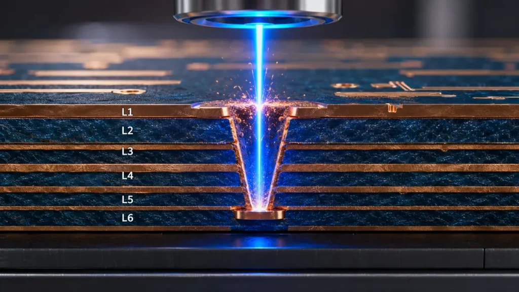
High-Precision UV Laser Drilling Microvia on 6-Layer HDI PCB (Cross-Section View)
The fabrication of blind and buried via PCBs demands a meticulously controlled multi-stage process that extends far beyond conventional multilayer manufacturing. Each step introduces variables that directly impact yield, reliability, and electrical performance.
Stage 1: Material Preparation & Stackup Engineering
Manufacturing begins with the selection and preparation of base materials. For blind via PCB production, the dielectric material must be “laser-drillable”—exhibiting consistent resin content and low glass weave distortion to ensure clean via formation. Common prepreg choices include:
- Standard FR-4: Cost-effective for 4–8 layer designs with moderate performance requirements
- High-Tg FR-4 (Tg ≥ 170°C): Essential for lead-free assembly compatibility and improved thermal reliability
- Low-Dk/Low-Df Materials (Megtron 6, Isola I-Tera MT40): Required for 25+ Gbps signal transmission
For buried via PCB fabrication, core materials are pre-drilled, plated, and etched as sub-assemblies before lamination. This “core-first” approach necessitates careful control of copper thickness, dielectric thickness, and dimensional stability to prevent layer-to-layer misalignment during the final press cycle.
Stage 2: Inner Layer Processing & Buried Via Formation
Buried vias are fabricated during the inner-layer stage. The process sequence includes:
- Mechanical Drilling: CNC drill machines create buried via holes in core laminates using carbide bits optimized for the specific material stack
- Desmear & Electroless Copper: Chemical processes remove drilling debris (smear) from via walls and deposit a thin (0.5–1.0 μm) electroless copper seed layer
- Electrolytic Copper Plating: DC acid copper plating builds barrel thickness to 20–25 μm, ensuring current-carrying capacity and mechanical integrity
- Pattern Plating & Etching: Photoresist imaging defines circuit traces; differential etching creates the final conductor geometry
At this stage, automated optical inspection (AOI) verifies trace width, spacing, and annular ring integrity before the cores proceed to lamination.
Stage 3: Sequential Lamination for Blind Via Integration
Sequential lamination is the defining process of HDI manufacturing. Rather than laminating all layers in a single press cycle, the board is built incrementally:
- First Lamination: Core sub-assemblies (with buried vias) are pressed with prepreg and copper foil
- Laser Drilling: UV/CO₂ lasers create blind microvias from the outer surface to the first internal layer
- Desmear & Plating: Microvias receive electroless copper seeding and electrolytic filling
- Pattern Definition: Outer layer circuits are imaged and etched
- Subsequent Laminations: For 2+N+2 or higher-order HDI, additional prepreg/copper layers are laminated, drilled, and plated in repeated cycles
Each lamination cycle introduces thermal stress that can cause material shrinkage. Advanced fabricators compensate using real-time scaling algorithms based on batch-specific material behavior data.
Stage 4: Laser Drilling Technology & Precision Control
Modern laser-drilled blind via production relies on dual-laser systems:
- CO₂ Laser (10.6 μm wavelength): Efficiently ablates organic dielectric materials (FR-4, polyimide) but reflects off copper
- UV Laser (355 nm wavelength): Removes copper foil with minimal heat-affected zone, achieving clean pad definition
The drilling process is controlled by automated optical alignment systems that reference existing copper features to achieve sub-micron positional accuracy. At Hongda Circuit, our laser systems are integrated with X-ray pre-alignment stations that verify core position before drilling, compensating for any material shift from previous processing steps.
Stage 5: Advanced Via Filling & Planarization
Via filling is critical for both electrical performance and assembly reliability. Two primary methodologies are employed:
- Copper Electroplating Fill A specialized DC acid copper formulation with leveling additives deposits copper from the via bottom upward, achieving complete fill without voids. This method provides the lowest electrical resistance and highest thermal conductivity, making it ideal for power delivery vias and thermal management applications. The process yields a planar via top with surface copper thickness of approximately 10 μm, eliminating the need for additional planarization steps.
- Conductive Epoxy Fill Silver-filled epoxy paste is screen-printed or dispensed into vias, then cured at elevated temperature. While offering higher resistance than solid copper, conductive epoxy provides adequate electrical continuity for signal vias and simplifies the manufacturing process. Non-conductive epoxy fill is also used where electrical isolation between filled vias and surrounding copper is required.
Stage 6: Quality Assurance—AOI, X-Ray & Electrical Testing
The inspection regime for blind and buried via PCBs is substantially more rigorous than for standard multilayer boards:
- Automated Optical Inspection (AOI): High-resolution cameras inspect outer layer traces for opens, shorts, and dimensional deviations. AI-enhanced AOI systems now achieve defect detection rates exceeding 99.9% while predicting potential reliability issues before they manifest as field failures.
- X-Ray Inspection: 2D and 3D X-ray systems verify blind via alignment, barrel integrity, and fill completeness without destructive testing. X-ray is the only non-destructive method capable of inspecting buried vias after lamination.
- Flying Probe Electrical Test: For prototypes and low-volume production, flying probe testers verify netlist continuity and isolation with programmable probe positioning.
- Fixture-Based ICT: High-volume production employs dedicated bed-of-nails fixtures for rapid electrical validation.
- Microsection Analysis: Destructive cross-sectioning of coupon boards verifies copper plating thickness, via fill quality, and layer-to-layer registration.
Stage 7: Reliability Validation
Before release to customers, representative samples undergo accelerated life testing:
- Interconnect Stress Test (IST): Thermal cycling between 25°C and 150°C evaluates via barrel integrity under thermomechanical stress
- Thermal Shock: Rapid temperature transitions (-65°C to +150°C) identify material adhesion weaknesses
- CAF (Conductive Anodic Filament) Resistance: High-humidity, high-voltage bias testing confirms resistance to electrochemical migration between biased conductors
Material Selection for High-Performance Blind & Buried Via PCBs
The substrate material determines overall electrical and thermal performance. Refer to our guide on PCB materials for blind via HDI designs for low-loss Megtron and Rogers laminates. Material selection must balance dielectric properties, processability, cost, and supply chain availability.
FR-4: The Industry Baseline
Standard FR-4 (Flame Retardant 4) remains the most widely used substrate for blind via applications up to 1 GHz. With a dielectric constant (Dk) of 4.2–4.8 and loss tangent (Df) of 0.020–0.025, FR-4 provides adequate performance for consumer electronics, industrial controls, and automotive modules where cost sensitivity predominates over extreme electrical performance.
For blind via PCB manufacturing, it is critical to specify “laser-drillable” FR-4 grades with uniform glass weave and controlled resin content. Inconsistent resin distribution can cause via wall roughness and plating voids that compromise long-term reliability.
High-Tg FR-4 (Tg ≥ 170°C)
High glass transition temperature (High-Tg) FR-4 is mandatory for designs subjected to lead-free solder reflow temperatures (peak 260°C) or extended operational thermal exposure. The elevated Tg reduces z-axis expansion during thermal cycling, minimizing via barrel stress and improving resistance to pad cratering and barrel cracking.
High-Tg FR-4 is the standard choice for automotive blind via PCBs (IATF 16949 applications), medical device PCBs (ISO 13485), and industrial automation systems where 10+ year operational lifetimes are required.
Megtron 6 & Megtron 7: Low-Loss Digital Substrates
Panasonic Megtron 6 (Dk ≈ 3.4, Df ≈ 0.002) and Megtron 7 (Dk ≈ 3.1, Df ≈ 0.001) represent the state-of-the-art for high-speed digital applications. These materials enable signal transmission at 56 Gbps PAM4 and 112 Gbps NRZ with acceptable insertion loss margins, making them indispensable for:
- AI server backplanes and accelerator modules
- 400G/800G optical transceivers
- 5G base station RF boards
- High-performance computing (HPC) interconnects
Megtron materials are fully compatible with laser drilling processes, though their modified epoxy chemistry requires optimized laser power parameters to prevent carbonization at via walls.
Rogers Corporation High-Frequency Laminates
Rogers RO4003C (Dk 3.38, Df 0.0027) and RO4350B (Dk 3.48, Df 0.0037) are ceramic-filled hydrocarbon laminates optimized for RF and microwave applications. These materials offer:
- Excellent dielectric constant stability across temperature and frequency
- Low moisture absorption (<0.1%)
- Compatible coefficient of thermal expansion (CTE) with copper
Rogers laminates are frequently specified in blind via PCB designs for aerospace radar systems, satellite communication payloads, and automotive 77 GHz radar modules. Hybrid stackups—combining Rogers for RF layers with FR-4 for digital/power layers—optimize cost while preserving RF performance.
Polyimide: Extreme Environment Durability
Polyimide substrates (Tg > 250°C) provide exceptional thermal stability and flexibility, making them the material of choice for:
- Aerospace and military avionics (MIL-PRF-31032, AS9100)
- Down-hole oil and gas instrumentation
- Medical implantable devices
Polyimide’s high-temperature capability comes with increased manufacturing complexity. Laser drilling parameters must be carefully controlled to prevent material charring, and plating chemistries require modification to achieve adequate adhesion to the polyimide surface.
Blind & Buried Via PCB Stackup Design Guide
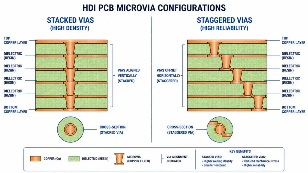
HDI PCB Microvia Architecture Comparison: Stacked Vias vs. Staggered Vias
Stackup architecture directly influences manufacturability, signal integrity, and cost. The following guidelines provide framework recommendations for common layer counts, with the understanding that specific designs may require customization based on component density and electrical requirements.
4-Layer Blind Via PCB Stackup
A 4-layer blind via PCB typically employs a 1+2+1 HDI structure:
| Layer | Function | Via Type |
|---|---|---|
| L1 (Top) | Signal / Components | Blind via to L2 |
| L2 | Ground Plane | — |
| L3 | Power Plane / Signal | — |
| L4 (Bottom) | Signal / Components | Blind via to L3 |
This configuration is ideal for IoT modules, compact industrial sensors, and consumer wearable devices. The 1+N+1 structure requires only a single sequential lamination cycle, keeping manufacturing costs competitive while achieving 30–40% routing density improvement over through-hole-only designs.
6-Layer Blind & Buried Via PCB Stackup
The 6-layer configuration introduces buried vias for internal connectivity:
| Layer | Function | Via Type |
|---|---|---|
| L1 (Top) | Signal / Components | Blind via to L2 |
| L2 | Signal | Buried via to L5 |
| L3 | Ground | — |
| L4 | Power | — |
| L5 | Signal | Buried via to L2 |
| L6 (Bottom) | Signal / Components | Blind via to L5 |
This 2+2+2 structure with buried vias connecting L2–L5 enables complex routing while maintaining dedicated power and ground planes for signal integrity. Typical applications include automotive ECUs, medical imaging controllers, and telecom interface cards.
8-Layer HDI Blind Via PCB Stackup
8-layer HDI designs commonly use 2+N+2 architecture:
| Layer | Function | Via Type |
|---|---|---|
| L1 (Top) | Signal / Components | Stacked microvia to L3 |
| L2 | Ground | — |
| L3 | Signal | Staggered microvia to L1/L5 |
| L4 | Power | — |
| L5 | Signal | Staggered microvia to L3/L7 |
| L6 | Ground | — |
| L7 | Signal | Stacked microvia to L5/L8 |
| L8 (Bottom) | Signal / Components | Stacked microvia to L7 |
The 2+N+2 structure supports fine-pitch BGA routing with via-in-pad technology. Stacked microvias on the outer layers provide high-density escape routing, while staggered vias on internal layers optimize reliability. This stackup is widely used in 5G smartphone motherboards, tablet computing platforms, and compact AI edge devices.
10-Layer & 12-Layer Multilayer Blind Via PCB Stackup
For 10-layer and 12-layer designs, 3+N+3 HDI with buried via cores becomes necessary:
- Core sub-assembly: Internal 4–6 layers with buried vias are fabricated and tested independently
- Sequential buildup: Three layers of microvia buildup on each side of the core
- Stacked/staggered hybrid: Outer layers use stacked vias for maximum density; inner buildup layers use staggered vias for reliability
These configurations support 0.4 mm pitch BGA devices, DDR5 memory interfaces, and multi-lane PCIe Gen5 routing. Manufacturing yields are sensitive to registration accuracy, requiring LDI imaging and automated optical alignment throughout the process.
16-Layer to 20+ Layer High-Layer-Count Buried Via PCB Stackup
High-layer-count buried via PCBs (16L, 20L, 26L+) represent the most demanding fabrication category. These boards typically employ:
- Multiple buried via cores: 2–4 core sub-assemblies, each with internal buried vias
- Sequential lamination: 4–5 press cycles for advanced AI server applications
- ELIC or near-ELIC capability: Microvias spanning 3–4 layers for ultra-dense routing
The NVIDIA GB300 AI server platform, for example, utilizes 70+ layer midplane/orthogonal backplane technology with interlayer registration controlled to within ±5 μm. These designs require specialized materials (Megtron 6/7), advanced laser drilling with real-time feedback, and comprehensive X-ray inspection at every lamination stage.
Critical Design Rules for Blind & Buried Via PCBs
Adherence to established design rules ensures that blind and buried via PCBs can be manufactured reliably while meeting electrical performance targets. The following parameters represent industry best practices refined through millions of production panels.
Via Diameter & Pad Sizing
| Via Type | Drilled Diameter | Finished Diameter | Capture Pad | Annular Ring (Min) |
|---|---|---|---|---|
| Laser microvia (blind) | 75–100 μm | 80–110 μm | 200–250 μm | 50 μm |
| Laser microvia (blind, fine pitch) | 100–125 μm | 110–135 μm | 250–300 μm | 75 μm |
| Mechanical blind via | 200–300 μm | 210–310 μm | 400–500 μm | 100 μm |
| Mechanical buried via | 200–350 μm | 210–360 μm | 400–550 μm | 100 μm |
| Via-in-pad (VIP) | 100–150 μm | 110–160 μm | = BGA pad size | 25 μm (after plating) |
Aspect Ratio Control
The aspect ratio (via depth divided by drilled diameter) is the single most critical manufacturability parameter:
- Laser microvias: Maximum aspect ratio 0.8:1 for void-free plating; 1:1 achievable with advanced chemistry
- Mechanical blind vias: Maximum aspect ratio 1:1
- Mechanical buried vias: Maximum aspect ratio 10:1 (standard); 12:1 (advanced)
Exceeding these ratios risks plating voids, barrel cracking, and inconsistent via fill—defects that may not be detected by electrical testing but will manifest as field failures under thermal stress.
Annular Ring & Pad Design
Annular ring—the copper pad area surrounding the drilled hole—provides the capture target for layer-to-layer registration. IPC-2226 specifies minimum annular ring requirements based on reliability class:
- IPC Class 2 (Industrial/Commercial): Minimum 0.05 mm annular ring
- IPC Class 3 (High Reliability): Minimum 0.075 mm annular ring
- IPC Class 3/A (Aerospace): Minimum 0.10 mm annular ring
For via-in-pad designs, the annular ring is effectively zero (the via occupies the entire pad). These designs require absolute registration confidence and complete via filling to prevent solder wicking during assembly.
Copper Thickness & Current Capacity
Copper plating thickness in via barrels directly impacts current-carrying capacity and thermal performance:
- Standard signal vias: 20–25 μm (0.8–1.0 mil) copper plating
- Power delivery vias: 30–50 μm (1.2–2.0 mil) or heavy copper fill
- Thermal vias: Solid copper fill or copper paste for maximum heat transfer
For high-current applications, multiple parallel vias or arrays of vias should be used to distribute thermal and electrical load.
Registration Accuracy & Layer-to-Layer Alignment
Registration—the alignment of drilled vias to their target capture pads across multiple lamination cycles—is the primary yield determinant in blind and buried via PCB manufacturing. Advanced registration techniques include:
- Non-linear scaling: Compensating for material-specific shrinkage patterns rather than applying uniform scaling factors
- LDI (Laser Direct Imaging): Real-time image adjustment based on actual copper feature positions, eliminating film-related errors
- X-ray pre-alignment: Verifying core position before laser drilling to compensate for shift from previous processing
At Hongda Circuit, our registration systems achieve layer-to-layer alignment within ±10 μm (±0.4 mil), enabling reliable production of 3+N+3 HDI with 75 μm microvias.
Signal Integrity Optimization in Blind & Buried Via PCBs
As data rates push beyond 56 Gbps PAM4 toward 112 Gbps and 224 Gbps aggregate channels, signal integrity (SI) engineering becomes inseparable from via design. Blind and buried vias offer intrinsic SI advantages that, when properly leveraged, can mean the difference between a functional first-spin design and a costly re-spin.
Return Path Continuity
Every high-speed signal requires a continuous, low-impedance return path. When a signal transitions through a via from one layer to another, its return current must find a path back to the source. If the reference plane changes (e.g., from ground to power), a return path discontinuity occurs, creating ground bounce and EMI.
Best practices for return path management:
- Stitching vias: Place ground vias adjacent to every signal via transition to provide a continuous return path
- Ground via fences: Surround high-speed differential pairs with ground vias spaced at λ/20 intervals to confine electromagnetic fields
- Anti-pad optimization: Size anti-pads (clearance holes in reference planes) to minimize capacitive coupling while avoiding excessive voids that interrupt return current flow
Impedance Control & Via Stub Elimination
Via stubs—the unused portion of a through-hole via extending beyond the active signal layer—act as resonant transmission line segments. At frequencies where the stub length equals λ/4, severe impedance discontinuities and signal reflections occur.
Blind vias inherently eliminate stubs by connecting only the layers actually used by the signal. For designs where through-hole vias are unavoidable, backdrilling (controlled depth drilling to remove stub material) reduces effective stub length to <0.15 mm, rendering stub resonance harmless for signals up to 28 Gbps.
For AI server PCB designs operating at 112 Gbps, blind microvias with zero stub length are the only viable via technology. The via itself still introduces parasitic capacitance (typically 0.1–0.3 pF) and inductance (0.3–0.8 nH), but these values are manageable through careful anti-pad sizing and dielectric material selection.
Crosstalk Mitigation in Dense Via Arrays
In high-density BGA fields, via-to-via crosstalk can dominate system noise margins. The electric and magnetic fields surrounding adjacent vias couple energy between signals, creating both near-end crosstalk (NEXT) and far-end crosstalk (FEXT).
Mitigation strategies:
- 3W rule: Maintain via-to-via spacing ≥3× the via diameter for uncoupled signals
- Orthogonal routing: Route adjacent signal layers perpendicular to each other to minimize broadside coupling
- Ground shielding: Insert grounded “guard vias” between aggressive and victim signal vias in critical paths
- Staggered via patterns: Offset vias between layers to reduce vertical coupling
High-Speed Design Considerations for 112G/224G Channels
At 112 Gbps PAM4 and 224 Gbps aggregate data rates, the interconnect physics become unforgiving. Every geometric discontinuity—via pads, anti-pads, trace width changes—contributes to channel degradation.
Advanced techniques for extreme high-speed designs:
- Elliptical vias: Orient via major axes parallel to trace directions to preserve field uniformity
- Solder mask defined pads: Reduce pad capacitance by allowing solder mask to overlap the pad edge
- Hybrid material stackups: Use Megtron 6 or Rogers for high-speed signal layers, FR-4 for power/ground to optimize cost-performance ratio
- AI-driven SI simulation: Modern design workflows employ machine learning models trained on field-solver data to predict via-induced discontinuities before layout commitment, reducing simulation time from hours to minutes
Reliability Testing & IPC Standards for Blind & Buried Via PCBs
The long-term reliability of blind and buried via PCBs is validated through rigorous stress testing. Read our dedicated guide on blind via reliability testing and IPC standards to evaluate IST, CAF, and thermal shock qualification protocols for high-density interconnects..
Interconnect Stress Test (IST)
IST subjects via interconnects to rapid thermal cycling between ambient and 150°C, typically for 500–1000 cycles. The test monitors resistance changes in via daisy chains; a resistance increase >10% indicates barrel cracking or pad delamination. IST is particularly effective at identifying latent defects in stacked microvia structures where thermal expansion mismatches between copper and dielectric can accumulate stress across multiple via levels.
Thermal Shock Testing
Thermal shock (per IPC-TM-650, Method 2.6.7) exposes test specimens to rapid temperature transitions between -65°C and +150°C, with dwell times as short as 5 minutes. This severe stress identifies weaknesses in material adhesion, plating ductility, and laminate integrity that gradual thermal cycling might not reveal. Automotive blind via PCBs and military-grade buried via PCBs typically require 100+ thermal shock cycles without failure.
CAF (Conductive Anodic Filament) Resistance
CAF is an electrochemical failure mechanism where conductive copper filaments grow along glass fiber/epoxy interfaces under the influence of humidity, voltage bias, and temperature. In high-density blind and buried via PCBs, the close proximity of biased conductors (fine-pitch vias, tight trace spacing) creates conditions conducive to CAF formation.
CAF resistance testing (85°C/85% RH, 100V DC bias, 1000+ hours) is mandatory for:
- Automotive electronics (under-hood environments)
- Medical devices (sterilization exposure)
- Telecom infrastructure (25-year operational life expectancy)
Material selection significantly impacts CAF performance. High-Tg, halogen-free laminates with enhanced resin systems demonstrate superior CAF resistance compared to standard FR-4.
IPC Standards Compliance
| IPC Standard | Scope | Relevance to Blind & Buried Vias |
|---|---|---|
| IPC-2226 | HDI PCB Design Standard | Defines microvia geometries, aspect ratios, and annular ring requirements |
| IPC-6012F | Rigid PCB Performance Specification | Qualification criteria for Class 2, Class 3, and Class 3/A products |
| IPC-6012E | HDI PCB Performance Addendum | Specific requirements for microvia integrity and sequential lamination |
| IPC-TM-650 | Test Methods Manual | Standardized test procedures for thermal stress, CAF, plating adhesion |
| IPC-4101 | Base Material Specification | Dielectric material qualification for laser drillability and reliability |
At Shenzhen Hongda Circuit Technology Co., Ltd., all blind and buried via PCBs are manufactured to IPC Class 2 as standard, with IPC Class 3 and IPC Class 3/A available for high-reliability applications. Our quality management system is certified to ISO 9001, IATF 16949 (automotive), ISO 13485 (medical), and AS9100D (aerospace), ensuring that every product meets the stringent requirements of its target industry.
Reliability Validation Protocol at Hongda Circuit
Our validation process extends beyond IPC minimums to include:
- 100% AOI + X-ray inspection on all HDI layers
- Microsection analysis on every production lot
- IST qualification for new stackup introductions
- CAF testing for automotive and medical product families
- Solder float testing (288°C, 10 seconds, 3 cycles) for thermal stress verification
- Temperature cycling (-40°C to +125°C, 1000 cycles) for automotive qualification
Cost Analysis: Blind Via PCB vs Buried Via PCB Manufacturing
Understanding cost drivers enables procurement teams to optimize total cost of ownership. Explore our comprehensive blind via PCB cost breakdown and price drivers to understand how sequential lamination and laser drilling cycles impact unit pricing
Laser Drilling Cost Factors
UV laser drilling represents a significant capital investment—modern dual-laser systems cost $1.5–3.0 million per unit. Operating costs include:
- Laser source maintenance: UV laser diodes require periodic replacement ($50,000–80,000 annually)
- Drill time: Microvia drilling at 120,000 holes/panel/hour; complex AI server panels may contain 500,000+ microvias
- Yield impact: Laser drilling parameters must be optimized per material type; incorrect settings cause via wall roughness that reduces plating yield
Cost impact: Laser drilling adds 20–35% to base manufacturing cost compared to mechanical drilling, but this is offset by the elimination of backdrilling operations and the ability to reduce layer count.
Sequential Lamination Cost Impact
Each sequential lamination cycle adds material, labor, and equipment time:
| HDI Order | Lamination Cycles | Cost Multiplier (vs. Standard ML) | Typical Applications |
|---|---|---|---|
| 1+N+1 | 2 | 1.2–1.4× | IoT, wearables, consumer |
| 2+N+2 | 3 | 1.5–1.8× | Smartphones, tablets, automotive |
| 3+N+3 | 4 | 2.0–2.5× | 5G infrastructure, AI edge |
| 4+N+4 / ELIC | 5+ | 2.5–4.0× | AI servers, high-end telecom |
The cost multiplier is non-linear because yield loss compounds with each additional lamination cycle. A 1% defect rate per cycle becomes a 4% cumulative loss for 4+N+4 structures. This makes supplier yield performance—rather than quoted unit price—the dominant factor in high-HDI total cost.
Yield Optimization Strategies
Hongda Circuit employs several strategies to maintain competitive yields on complex blind and buried via PCBs:
- Predictive process control: AI-driven monitoring of etching stability, drill accuracy trends, and plating thickness consistency flags drift before it becomes scrap
- Non-linear artwork scaling: Real-time compensation for material shrinkage based on batch-specific behavior data
- Digital twin simulation: Virtual validation of new stackups before physical production, reducing NRE (Non-Recurring Engineering) costs by 30–40%
- Flexible manufacturing: Production lines accommodating volumes from 1 prototype to 100,000+ units, with urgent prototypes deliverable in 8 hours for qualified designs
Material Cost Considerations
| Material | Cost Index (FR-4 = 1.0) | Primary Value Proposition |
|---|---|---|
| Standard FR-4 | 1.0 | Cost optimization for low-speed applications |
| High-Tg FR-4 | 1.2–1.4 | Lead-free assembly compatibility, improved thermal reliability |
| Megtron 6 | 4.0–5.0 | 56G/112G signal integrity, low insertion loss |
| Megtron 7 | 6.0–8.0 | 224G+ channels, AI server backplanes |
| Rogers RO4003C | 5.0–7.0 | RF/microwave performance, stable Dk |
| Polyimide | 3.0–5.0 | Extreme temperature durability, flexibility |
For most designs, a hybrid stackup—using premium materials only for critical signal layers and standard FR-4 for power/ground—delivers 80% of the performance benefit at 40% of the full-premium cost.
Testing & Inspection Cost Allocation
The inspection burden for blind and buried via PCBs is substantially higher than for standard multilayer boards:
- AOI: 100% outer layer inspection (standard for all products)
- X-ray inspection: Required for blind/buried via integrity verification; adds 5–10% to processing cost
- Microsection analysis: Destructive testing on coupon boards; adds material and labor cost
- Electrical test: Flying probe (prototypes) or fixture ICT (volume); fixture cost amortized over production volume
Despite these additive costs, the total system cost often favors HDI designs because:
- Reduced PCB size (30–50% smaller) lowers enclosure and mechanical costs
- Fewer layers (e.g., 8L HDI vs. 12L standard) reduce material consumption
- Improved signal integrity reduces EMI shielding and filtering component requirements
- Higher routing density enables single-board solutions vs. multi-board interconnects
Industry Applications of Blind & Buried Via PCBs
The adoption of blind and buried via PCB technology spans virtually every high-performance electronics sector. The following application profiles illustrate how specific industries leverage these interconnect solutions.
AI Server & Data Center Infrastructure
The explosive growth of AI computing—global AI server shipments projected to exceed 2 million units in 2026—has made AI server PCBs the most demanding application for blind and buried via technology. A single AI server motherboard may contain:
- 20–40+ layer count with 4+N+4 or ELIC HDI structures
- 500,000+ microvias connecting 0.35 mm pitch GPUs and HBM modules
- 112 Gbps PAM4 signal channels requiring zero-stub via transitions
- Megtron 6/7 substrates for acceptable insertion loss at 56 GHz Nyquist frequencies
The PCB content value of an AI server is nearly ten times that of a conventional server, making this the highest-growth segment for advanced PCB manufacturers. Supply constraints remain acute, with high-end PCB lead times extending 18–24 months for new product introductions.
Aerospace & Military Systems
Aerospace blind via PCBs and military buried via PCBs prioritize reliability over cost. Applications include:
- Satellite communication payloads: Rogers substrates with blind vias for Ka-band and V-band transceivers
- Radar systems: Multilayer buried via boards with polyimide substrates for phased array antennas
- Avionics flight computers: IPC Class 3/A qualification with IST and thermal shock validation
These applications typically specify AS9100D quality management, IPC-J-STD-001 soldering requirements, and MIL-PRF-31032 material traceability.
Medical Electronics
Medical device PCBs demand a unique combination of miniaturization, reliability, and biocompatibility:
- Implantable devices: Polyimide flexible-rigid boards with blind vias for pacemakers and neurostimulators
- Medical imaging: High-layer-count buried via PCBs for CT and MRI data acquisition systems
- Surgical robotics: HDI blind via boards for motor control and sensor interfaces
ISO 13485 certification and biocompatibility testing (ISO 10993) are mandatory for medical PCB suppliers.
Automotive Electronics
The electrification and autonomy trends in automotive are driving unprecedented PCB complexity:
- ADAS sensor fusion modules: 10+ layer HDI with blind vias for camera, radar, and LiDAR data processing
- Battery management systems (BMS): Heavy copper buried vias for high-current cell balancing
- Domain controllers: 2+N+2 HDI with staggered vias for zonal E/E architectures
Automotive PCBs must meet IATF 16949, AEC-Q100 component qualification, and operational temperature ranges of -40°C to +125°C (Grade 1) or -40°C to +150°C (Grade 0).
Telecommunications & Networking
5G base stations, 400G/800G optical transceivers, and core routers represent the traditional stronghold of blind and buried via technology:
- 5G mmWave: Rogers hybrid stackups with blind vias for 28 GHz and 39 GHz RF paths
- Optical modules: 2+N+2 HDI with via-in-pad for 56G/112G electrical interfaces
- Core routers: 20+ layer buried via backplanes with impedance control to ±3%
Industrial Control & Automation
Industrial applications emphasize long-term reliability in harsh environments:
- PLC controllers: High-Tg FR-4 with blind vias for compact I/O modules
- Motor drives: Heavy copper buried vias for power stage integration
- IoT edge gateways: 1+N+1 HDI for wireless connectivity + sensor aggregation
Why Choose Shenzhen Hongda Circuit Technology Co., Ltd. for Your Blind & Buried Via PCB Requirements
Shenzhen Hongda Circuit Technology Co., Ltd. has established itself as a premier blind via manufacturer and buried via PCB manufacturer, serving global OEMs across AI, aerospace, medical, automotive, and telecommunications markets. Our competitive differentiation is built on four pillars:
Advanced HDI Manufacturing Capability
- Laser drilling: Mitsubishi UV/CO₂ dual-laser systems with 75 μm minimum via diameter and ±15 μm positional accuracy
- Sequential lamination: 5+ press cycles supporting 4+N+4 and ELIC architectures
- Via filling: Proprietary copper electroplating chemistry achieving void-free fill with planar surface finish
- Registration: LDI imaging with non-linear scaling and X-ray pre-alignment, maintaining ±10 μm layer-to-layer registration
Comprehensive Quality Assurance
- AI-enhanced AOI: Defect detection rates >99.9% with predictive reliability analysis
- 3D X-ray inspection: Non-destructive verification of blind/buried via integrity, alignment, and fill completeness
- Flying probe & ICT electrical test: 100% netlist verification for all production panels
- Accelerated life testing: In-house IST, thermal shock, and CAF testing capabilities
Industry Certifications & Compliance
| Certification | Scope | Relevance |
|---|---|---|
| ISO 9001:2015 | Quality Management | Foundation for all operations |
| IPC Class 2/3/3A | PCB Performance | Standard to aerospace reliability grades |
| IATF 16949:2016 | Automotive QMS | Tier 1 automotive supplier qualification |
| ISO 13485:2016 | Medical Device QMS | FDA-regulated medical product manufacturing |
| AS9100D | Aerospace QMS | Defense and commercial aviation programs |
| UL Certification | Safety Compliance | North American market access |
| RoHS/REACH | Environmental Compliance | EU and global environmental regulations |
Flexible Production & Rapid Prototyping
- Prototype-to-volume continuum: Single-piece prototypes to 100,000+ unit annual volumes on shared production lines
- Fast-turn capability: 24–48 hour prototype delivery for qualified HDI designs; 8-hour emergency builds available
- DFM partnership: Dedicated engineering team providing stackup optimization, impedance modeling, and manufacturability review before design release
- Global logistics: Shenzhen manufacturing base with distribution hubs in North America, Europe, and Southeast Asia
Frequently Asked Questions (FAQ) — Procurement & Technical Guide
How do I verify a blind via PCB manufacturer’s actual HDI capability before placing an order?
Verify supplier real HDI capacity with 5 key steps:
Request equipment list — Ask for laser drill brand/model (Mitsubishi, ESI, LPKF top-tier), minimum drill size, position accuracy data
Ask for registration data — Require actual layer alignment test data (≤±15μm qualified, ≤±10μm excellent)
Review certification scope — Validate valid IPC Class 3, ISO 9001, IATF 16949 certificates with full scope
Demand cross-section photos — Request microsection samples from past projects to check via fill uniformity and copper thickness
Pilot build with full report — Order 5–10pcs trial run, require complete X-ray, AOI, IST test reports
Red flag: If supplier refuses microsection/X-ray reports or claims all customer data is confidential, avoid cooperation.
What is the typical cost premium for blind and buried via PCBs versus standard multilayer boards?
The cost premium depends on HDI complexity: 1+N+1 structures add 20–40%; 2+N+2 adds 50–80%; 3+N+3 and above can double or triple the base cost. However, the total system cost often decreases because HDI enables smaller board sizes, fewer total layers, reduced EMI shielding, and elimination of multi-board interconnects. For high-volume consumer electronics, the per-unit cost increase is frequently offset by enclosure and assembly savings.
How do I verify that a PCB manufacturer can reliably produce blind and buried via boards?
Evaluate four critical capabilities: (1) Equipment portfolio—UV laser drills, sequential lamination presses, LDI imaging systems; (2) Registration performance—request data on layer-to-layer alignment accuracy (should be ≤±15 μm for HDI); (3) Quality certifications—IPC Class 3, ISO 9001, and industry-specific certifications (IATF 16949, ISO 13485, AS9100); (4) Testing infrastructure—3D X-ray inspection, IST capability, and microsection analysis facilities. Request a pilot build with full cross-sectional analysis before committing to volume production.
What materials are best for high-speed blind via PCBs operating above 25 Gbps?
For 25–56 Gbps channels, Panasonic Megtron 6 (Dk 3.4, Df 0.002) provides optimal cost-performance balance. For 112 Gbps and beyond, Megtron 7 (Dk 3.1, Df 0.001) or Isola I-Tera MT40 are recommended. Hybrid stackups using premium materials for signal layers and standard FR-4 for power/ground reduce cost by 40–60% compared to all-premium constructions while preserving electrical performance.
What is the minimum trace and space achievable with blind via HDI technology?
Standard Type II HDI (1+N+1) supports 75 μm (3 mil) trace/space. Type III (2+N+2) achieves 50 μm (2 mil). Advanced ELIC (Every Layer Interconnection Capable) technology reaches 30 μm (1.2 mil) or finer, comparable to IC substrate manufacturing. These geometries require LDI imaging, ultra-thin copper foils, and advanced etching chemistries to maintain dimensional tolerance.
About Author
David Chen https://www.linkedin.com/in/pcbcoming
David Chen boasts an extensive professional background in PCBA manufacturing, PCBA testing, and PCBA optimization, with specialized expertise in high-precision PCBA fault analysis and rigorous PCBA reliability testing. The author has worked with high-layer-count server PCB fabrication, ultra-low-loss backplane stackups, and thermo-mechanical reliability optimization for AI infrastructure projects involving 112G and 224G PAM4 architectures. Skilled in complex circuit design and cutting-edge advanced PCB manufacturing processes, he delivers solutions that elevate product durability and performance across industrial applications. His technical articles focusing on PCBA manufacturing workflows and testing methodologies are widely cited by industry peers, research institutions, and technical platforms, solidifying his reputation as a recognized technical authority in the global circuit board manufacturing sector.