Blind Via PCB Materials: Complete Selection Guide for HDI, High-Speed & High-Reliability Applications
Table of Contents
- What Materials Are Used in Blind Via PCB?
- Why Material Selection Matters for Blind Via PCB Manufacturing
- FR4 for Blind Via PCB: Standard vs High Tg Options
- Low Loss Materials for High-Speed Blind Via PCB
- Polyimide Material for Blind Via PCB
- PTFE Material for Blind Via PCB
- Material Comparison: FR4 vs Low Loss vs Polyimide vs PTFE
- How to Select Blind Via PCB Material for Your Project
- Blind Via PCB Materials for Different Applications
- PCB Material Selection Mistakes to Avoid
- How Shenzhen Hongda Circuit Supports Blind Via PCB Material Selection
- FAQ for Procurement Engineers
- To learn more about total manufacturing capabilities, check our https://www.pcbkr.com/blind-buried-via-pcb-manufacturing/ guide.
What Materials Are Used in Blind Via PCB?
Blind via PCB technology sits at the intersection of structural engineering and materials science. Unlike through-hole vias that penetrate the entire board, blind vias connect only specific layer pairs—typically from an outer surface to one or more internal layers. This structural distinction makes material selection far more consequential than in standard multilayer designs.
At Shenzhen Hongda Circuit Technology Co., Ltd., we process blind via PCBs across six primary material categories, each engineered for distinct thermal, electrical, and mechanical demands:
| Material Category | Glass Transition (Tg) | Dk @ 10 GHz | Df @ 10 GHz | Primary Applications |
|---|---|---|---|---|
| Standard FR-4 | 130–140°C | 4.2–4.7 | 0.015–0.020 | Consumer electronics, industrial controllers |
| High Tg FR-4 | 170–180°C | 4.0–4.5 | 0.012–0.016 | Automotive ECU, power electronics |
| Low Loss (Megtron 6/7/8) | 185–200°C | 3.4–3.7 | 0.0015–0.003 | AI servers, 112G/224G networking |
| Ultra-Low Loss (M9/M10) | ≥200°C | 3.0–3.3 | 0.0005–0.001 | Next-gen AI, 448G switches |
| Polyimide | ≥250°C | 3.2–3.5 | 0.002–0.004 | Aerospace, military, flex-rigid HDI |
| PTFE / Teflon | 327°C (melting) | 2.1–2.3 | 0.0002–0.0005 | 5G/6G RF, radar, microwave |
| Ceramic Hybrid | 200–300°C | 3.0–4.0 | 0.001–0.003 | High-power LED, automotive radar |
The material you choose directly governs four critical manufacturing outcomes: laser drilling quality, sequential lamination reliability, signal integrity performance, and long-term thermal stability. In 2026, with AI server architectures pushing 224G PAM4 signaling and automotive electronics facing 150°C under-hood environments, material selection has evolved from a secondary consideration to a primary engineering decision.
Why Material Selection Matters for Blind Via PCB Manufacturing
Laser Drilling Performance and Via Wall Quality
Blind vias in HDI boards are created using UV (355 nm) or CO₂ laser ablation systems. The material’s resin composition, glass weave density, and copper foil profile determine how cleanly the laser can ablate dielectric without damaging the capture pad beneath.
At Hongda Circuit, our Mitsubishi Electric UV/CO₂ hybrid laser drilling machines achieve microvia diameters down to 50 µm. However, material characteristics significantly influence outcomes:
- Resin homogeneity: Materials with uneven resin distribution (common in lower-grade FR-4) create inconsistent via wall roughness, increasing plating defects
- Glass weave style: Standard 7628 glass styles challenge CO₂ lasers; low-Dk Q-glass cloth (used in M9 laminates) ablates more uniformly
- Copper foil profile: HVLP5 ultra-low-profile copper foil (surface roughness <1.5 µm) reduces signal attenuation but requires precise laser energy calibration to avoid pad delamination
Our production data shows that M9-grade laminates with hydrocarbon/modified PPO resin systems and Q-glass cloth reduce laser drilling variability by 34% compared to standard FR-4, directly improving first-pass yield on 6+N+6 HDI builds.
Sequential Lamination Reliability in Multi-Cycle Builds
High-density interconnect PCBs often require 1+N+1, 2+N+2, or even 6+N+6 sequential lamination architectures. Each lamination cycle exposes the material to 180–200°C temperatures and 250–400 PSI pressure. Materials must withstand these conditions repeatedly without:
- Z-axis expansion that degrades via barrel integrity
- Resin flow that creates voids in filled microvias
- Dimensional drift that misaligns layer-to-layer registration
Hongda Circuit’s LAUFFER lamination systems operate with vacuum levels below 50 mbar and temperature uniformity within ±2°C across the full press area. For M9/M10 materials, we have developed proprietary lamination recipes that account for the lower resin flow characteristics of hydrocarbon-based systems, maintaining interlayer dielectric thickness within ±5% across 7+ sequential lamination cycles.
Signal Integrity at 112G and 224G PAM4
At data rates exceeding 56 Gbps, dielectric loss becomes the dominant signal degradation mechanism. The relationship is straightforward: higher dissipation factor (Df) equals greater insertion loss per inch of trace length.
For a 224G PAM4 channel operating at 56 GHz Nyquist frequency:
- Standard FR-4 (Df ≈ 0.018) generates approximately 1.2 dB/inch insertion loss
- Megtron 7 (Df ≈ 0.0017) reduces this to approximately 0.35 dB/inch
- M9-grade material (Df ≈ 0.0008) achieves under 0.25 dB/inch
This 5× reduction in dielectric loss is not incremental—it is the difference between a functional design and a failed prototype. Hongda Circuit’s Hisun-Test SIF-2001 automatic impedance test system, paired with Keysight VNA up to 67 GHz, verifies that every production panel meets the insertion loss budgets specified in IEEE 802.3df and OIF-CEI-112G standards.
FR4 for Blind Via PCB: Standard vs High Tg Options
Standard FR-4 for Cost-Sensitive Blind Via Applications
Standard FR-4 remains the workhorse material for blind via PCBs in consumer electronics, industrial control systems, and IoT devices where signal frequencies remain below 5 GHz. Its advantages are well-understood: mature supply chains, broad fabricator compatibility, and the lowest material cost per square meter in the industry.
However, standard FR-4 presents clear limitations for blind via HDI:
- Higher dielectric loss restricts usable bandwidth to approximately 3–5 GHz
- Moderate Tg (130–140°C) risks via barrel cracking during lead-free reflow at 260°C peak
- Greater Z-axis CTE (typically 50–70 ppm/°C above Tg) stresses plated via structures during thermal cycling
At Hongda Circuit, we recommend standard FR-4 for blind via designs only when:
- Layer count remains at or below 8 layers
- Operating frequencies stay below 3 GHz
- Board thickness is under 1.6 mm
- Cost is the primary decision driver
High Tg FR-4 for Automotive and Industrial Blind Via PCB
High Tg FR-4 (glass transition temperature ≥170°C) addresses the thermal reliability gaps of standard material without the cost premium of low-loss laminates. The modified epoxy resin systems used in High Tg grades deliver:
- Improved dimensional stability during sequential lamination, reducing layer-to-layer misregistration
- Better copper adhesion to via walls, critical for blind via plating integrity
- Enhanced resistance to CAF (Conductive Anodic Filament) growth in humid environments
Our automotive customers specify High Tg FR-4 for blind via PCBs in engine control modules, battery management systems, and ADAS sensor interfaces. These applications demand IPC Class 2 or Class 3 reliability through 1,000+ thermal cycles (-40°C to +125°C), which High Tg FR-4 consistently delivers when paired with our controlled-depth back-drilling and via-filling processes.
Low Loss Materials for High-Speed Blind Via PCB
Why AI Server PCBs Cannot Use Standard FR-4
The transition from 112G to 224G PAM4 signaling has rendered standard FR-4 obsolete for AI server backplanes and switch fabrics. At 56 GHz Nyquist frequency, the cumulative insertion loss across a 30-inch backplane channel exceeds 15 dB with FR-4—far beyond the 12 dB budget that PCIe 6.0 and Ethernet 802.3df specifications allow.
Low-loss materials solve this through three material science innovations:
- Hydrocarbon and modified PPO resin systems replace traditional epoxy, reducing molecular polarization losses
- Low-Dk Q-glass cloth (quartz-reinforced) replaces E-glass, cutting dielectric constant from 4.5 to 3.2–3.5
- HVLP4/5 copper foil with surface roughness below 1.5 µm minimizes skin effect losses at millimeter-wave frequencies
Megtron 6, Megtron 7, and the New M9/M10 Generation
Panasonic’s Megtron series has become the de facto standard for high-speed blind via PCBs. The progression from Megtron 6 to M10 reflects the industry’s relentless push for lower loss:
| Material | Dk @ 10 GHz | Df @ 10 GHz | Target Data Rate | Hongda Circuit Status |
|---|---|---|---|---|
| Megtron 6 | 3.7 | 0.002 | 56G/112G PAM4 | Full production, bonded inventory |
| Megtron 7 | 3.4 | 0.0017 | 112G/224G PAM4 | Full production, bonded inventory |
| Megtron 8 | 3.3 | 0.0012 | 224G PAM4 | Production qualified |
| M9 Grade | 3.0 | 0.0008 | 224G/448G PAM4 | Mass production (2026) |
| M10 Grade | ≤3.0 | <0.0008 | 448G+ / Rubin Ultra | Engineering samples |
Hongda Circuit is among the first Chinese manufacturers to achieve mass-production capability with M9-grade laminates. Our facility maintains bonded inventory of Panasonic Megtron 6/7/8, Isola Tachyon 100G, and Doosan ultra-low-loss materials, ensuring 24-hour material availability for fast-turn AI server prototypes.
M9-Grade Laminate: The 2026 Breakthrough
2026 marks the first year of large-scale M9 material deployment, driven by NVIDIA’s Rubin/VR300 platform requirements. M9 laminates are not simply “better Megtron”—they represent a fundamental shift in substrate architecture:
- Resin system: High-purity PPO/hydrocarbon blend (not epoxy-based)
- Reinforcement: High-purity quartz cloth (Q-cloth) rather than glass fiber
- Copper foil: HVLP5 with Ra ≤0.4 µm surface roughness
- Performance: 40% lower signal loss than M8 at 28 GHz
Hongda Circuit’s M9 qualification data shows consistent Dk stability within ±0.02 across the -40°C to +125°C temperature range—a critical requirement for AI server environments where chassis temperatures can swing 60°C between idle and full-load conditions.
Polyimide Material for Blind Via PCB
Why Aerospace and Defense Specify Polyimide
Polyimide stands apart from all other blind via PCB materials in one respect: it does not melt. With a decomposition temperature exceeding 500°C and continuous operating capability at 200–250°C, polyimide is the only practical choice for aerospace electronics, military avionics, and down-hole oil exploration tools.
For blind via HDI applications, polyimide offers unique advantages:
- Thermal cycling endurance: Survives 2,000+ cycles from -65°C to +150°C without via barrel cracking
- Flexural strength: Enables rigid-flex HDI designs where blind vias transition between rigid and flexible regions
- Chemical resistance: Withstands harsh cleaning solvents and conformal coating processes
- Low outgassing: Meets NASA ASTM E595 requirements for spaceflight electronics
Manufacturing Considerations for Polyimide Blind Via PCBs
Polyimide’s strengths come with manufacturing challenges that require specialized equipment and process knowledge:
- Laser drilling: Polyimide ablates differently than FR-4; UV lasers (355 nm) are preferred over CO₂ for cleaner via walls
- Desmear: Alkaline permanganate desmear must be carefully controlled—over-processing attacks polyimide resin
- Plating adhesion: Polyimide’s smooth surface requires plasma activation before electroless copper deposition
- Dimensional stability: High moisture absorption (1.5–2.0%) necessitates pre-bake before lamination
At Hongda Circuit, our polyimide blind via process has been qualified to IPC-6012DS (Space and Military Avionics Applications) with demonstrated capability for 4+N+4 rigid-flex HDI builds using DuPont Pyralux AP and Panasonic Felios materials.
PTFE Material for Blind Via PCB
PTFE for RF and Microwave Blind Via Applications
Polytetrafluoroethylene (PTFE)—commonly known by the brand name Teflon—delivers the lowest dielectric loss of any commercially available PCB substrate. With Dk ≈ 2.1 and Df as low as 0.0002, PTFE is the material of choice for:
- 5G/6G base station antenna arrays operating at 28 GHz and 39 GHz
- Automotive radar at 77–81 GHz
- Satellite communication transceivers
- High-frequency test fixtures requiring minimal signal distortion
Rogers and Taconic PTFE Laminates for Blind Via HDI
Pure PTFE is mechanically soft and thermally challenging to process. Commercial PTFE laminates from Rogers Corporation (RO3000, RO4000 series) and Taconic (TLX, TLY series) use ceramic fillers to improve mechanical stability and thermal conductivity while maintaining ultra-low loss.
For blind via HDI applications, Rogers RO4835+ and Taconic TLY-5Z have emerged as the leading choices:
- RO4835+: Dk 3.48, Df 0.0037, optimized for 77 GHz automotive radar
- TLY-5Z: Dk 2.2, Df 0.0009, preferred for 5G mmWave antenna-in-package designs
Hongda Circuit processes PTFE blind via PCBs using proprietary plasma desmear recipes and controlled lamination profiles that prevent PTFE’s tendency to cold-flow under pressure. Our 2026 capability includes 2+N+2 PTFE HDI with laser-drilled microvias down to 100 µm and impedance control within ±5%.
The Cost Reality of PTFE Blind Via PCBs
PTFE laminates cost 8–15× more than standard FR-4 per square meter. This cost multiplier is justified only when:
- Operating frequencies exceed 10 GHz
- Insertion loss budgets are tighter than 0.5 dB/inch
- Phase stability across temperature is critical (±0.5° typical for PTFE vs ±3° for FR-4)
For procurement engineers evaluating PTFE blind via suppliers, verify that the fabricator has dedicated PTFE process lines—cross-contamination from FR-4 processing can degrade PTFE’s electrical performance.
Material Comparison: FR4 vs Low Loss vs Polyimide vs PTFE
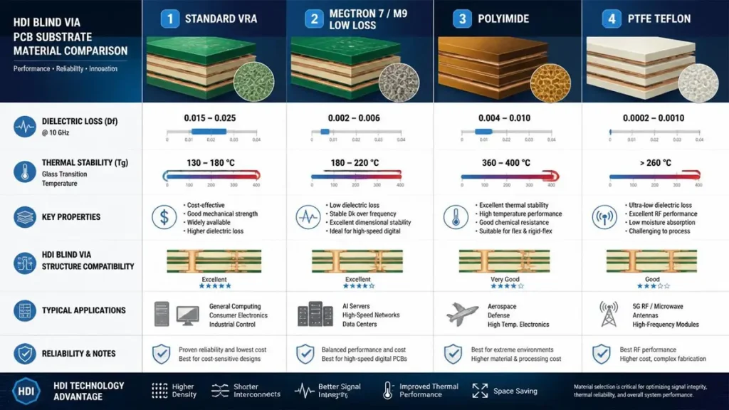
HDI Blind Via PCB Substrate Material Comparison Matrix
The following matrix provides a procurement-focused comparison for blind via PCB material selection:
| Evaluation Factor | FR-4 | Low Loss (Megtron/M9) | Polyimide | PTFE |
|---|---|---|---|---|
| Material Cost | $ (Baseline) | $$ – $$$$$ | $$$$ | $$$$$$ |
| Signal Integrity @ >10 GHz | Poor | Excellent | Good | Excellent |
| Thermal Stability | Moderate (Tg 140°C) | High (Tg 200°C) | Excellent (Tg >250°C) | High (melting 327°C) |
| HDI Blind Via Compatibility | Good | Excellent | Excellent | Moderate |
| Sequential Lamination Cycles | 3–4 max | 6–8 | 4–6 | 2–3 |
| Manufacturing Lead Time | 5–7 days | 7–10 days | 10–14 days | 12–18 days |
| Typical Applications | Consumer, industrial | AI server, networking | Aerospace, military | 5G RF, radar |
| DFM Complexity | Low | Medium | High | Very High |
Procurement Insight: The total cost of ownership for blind via PCBs extends beyond material price. Low-loss materials reduce layer count requirements (saving lamination cycles), improve first-pass yield (reducing scrap), and eliminate signal integrity redesigns. For a 12-layer AI server board, Megtron 7 may add $80–120 in material cost but save $300+ in engineering iteration and yield loss.
How to Select Blind Via PCB Material for Your Project
Decision Framework for Material Selection
Choose Standard FR-4 if:
- Budget is the primary constraint
- Operating frequency is below 3 GHz
- Layer count is 8 or fewer
- Operating temperature remains below 105°C
- Product lifecycle is under 5 years
Choose High Tg FR-4 if:
- Automotive or industrial temperature range (-40°C to +125°C)
- Moderate layer count (8–16 layers) with blind vias
- Lead-free assembly processes (260°C peak reflow)
- CAF resistance is required for humid environments
Choose Low Loss (Megtron 6/7/8) if:
- Data rates exceed 25 Gbps (56G/112G/224G PAM4)
- AI server, data center, or high-speed networking equipment
- Insertion loss budget is critical
- Layer count exceeds 16 layers with sequential lamination
Choose M9/M10 if:
- Next-generation AI platforms (NVIDIA Rubin, AMD MI400)
- 224G PAM4 or 448G PAM4 signaling
- Orthogonal backplane or midplane architectures
- Chassis-level thermal cycling from -40°C to +85°C
Choose Polyimide if:
- Aerospace, military, or spaceflight applications
- Operating temperature exceeds 150°C continuously
- Rigid-flex HDI with blind via transitions
- Outgassing requirements per NASA ASTM E595
Choose PTFE if:
- RF/microwave frequencies exceed 10 GHz
- 5G/6G antenna, radar, or satellite communication
- Phase stability across temperature is critical
- Dielectric loss must be minimized at all cost
Material Qualification Checklist for Procurement
Before committing to a blind via PCB supplier, request documentation on:
- Material traceability: Lot numbers, manufacturer C of C, UL file numbers
- Shelf life verification: Prepregs older than 90 days require re-qualification
- Thermal cycling data: IPC-TM-650 2.6.7 results for your specific stackup
- Impedance validation: TDR test reports with statistical process control data
- Microsection analysis: Cross-section photos showing via fill, plating thickness, and layer alignment
Hongda Circuit provides all five documentation items as standard deliverables for every production lot, with digital certificates accessible through our customer portal.
Blind Via PCB Materials for Different Applications
AI Server PCB Material Requirements
AI server PCBs represent the most demanding application for blind via materials in 2026. A typical NVIDIA GB300-class board requires:
- 32–70 layers with 6+N+6 or 7+N+7 sequential lamination
- 224G PAM4 signaling across 30+ inch channel lengths
- M9-grade laminates with Df ≤0.001 and Dk stability ±0.02
- HVLP5 copper foil for skin effect management
- Back-drilled vias with stub control within ±25 µm
Hongda Circuit’s AI server production line operates with SCREEN Ledia LDI exposure, Mitsubishi UV/CO₂ laser drilling, and LAUFFER vacuum lamination systems. Our 2026 capability extends to 104-layer backplanes with 224G PAM4 validation, supported by Keysight VNA testing to 67 GHz.
Automotive HDI PCB Material Selection
Automotive blind via PCBs face a unique combination of thermal, mechanical, and chemical stresses:
- Under-hood temperatures reaching 150°C in EV battery enclosures
- Vibration profiles per ISO 16750-3 (random 10 g RMS)
- Thermal shock from -40°C to +125°C in under 60 seconds
- Electrochemical migration resistance for 15-year service life
High Tg FR-4 (Tg ≥170°C) remains the baseline for automotive blind via HDI, with selective use of ceramic-filled materials for high-voltage isolation in 800V EV architectures. Hongda Circuit is IATF 16949:2016 certified and maintains PPAP Level 3 documentation for all automotive production programs.
Aerospace PCB Material Standards
Aerospace blind via PCBs must comply with IPC-6012DS or AS9100D standards, requiring:
- Polyimide or cyanate ester base materials
- Blind via plating minimum 25 µm copper thickness
- Thermal vacuum outgassing <1.0% TML and <0.1% CVCM
- Radiation tolerance for space applications (>100 krad total dose)
Hongda Circuit’s aerospace production cell operates under AS9100D with dedicated equipment, segregated material storage, and 100% lot traceability. Our polyimide blind via capability includes 4+N+4 rigid-flex builds qualified to IPC-6012DS Class 3.
RF and 5G PCB Material Considerations
5G mmWave and 6G sub-THz applications push blind via materials into uncharted territory:
- 28 GHz and 39 GHz antenna arrays require Df <0.003
- 77–81 GHz automotive radar demands phase stability within ±1°
- Dk uniformity across the panel must be within ±0.05 for beamforming accuracy
PTFE and ceramic-filled hydrocarbon materials (Rogers RO4835+, Taconic TLY-5Z) are the only viable options. Hongda Circuit’s RF blind via process achieves 50 µm line/space on PTFE substrates with laser-drilled microvias at 100 µm diameter, validated through S-parameter testing to 110 GHz.
PCB Material Selection Mistakes to Avoid
Mistake 1: Specifying FR-4 for High-Speed Blind Via Designs
The most expensive mistake in blind via procurement is selecting FR-4 for designs that require low-loss materials. The “savings” of $50–100 per panel in material cost are erased by:
- Signal integrity failures requiring layer count increases
- Re-spins due to excessive insertion loss
- Field failures from thermal cycling-induced via cracking
Rule of thumb: If your design includes 112G PAM4 or faster signaling, FR-4 is not an option—regardless of budget pressure.
Mistake 2: Ignoring Dk Variation Across Temperature and Frequency
Dielectric constant is not a single number. It varies with:
- Temperature: Dk can shift 5–10% from -40°C to +125°C
- Frequency: Dk typically decreases 3–5% from 1 GHz to 10 GHz
- Moisture absorption: Humidity can increase Dk by 2–4%
Hongda Circuit provides Dk/Df characterization data across temperature and frequency for all qualified materials, enabling accurate SI simulation before fabrication.
Mistake 3: Overlooking Lamination Compatibility
Not all materials laminate well together. Mixing FR-4 cores with low-loss prepregs in the same stackup creates CTE mismatches that generate internal stress during thermal cycling. Our engineering team reviews every stackup for material compatibility before releasing to production.
Mistake 4: Selecting Material Without Manufacturer Validation
A material data sheet is not a manufacturing qualification. Before specifying M9, polyimide, or PTFE for blind via HDI, confirm that your fabricator has:
- Process qualification for that specific material grade
- Bonded inventory to prevent supply disruptions
- Microsection data showing via quality on that material
- Reliability test results (thermal cycling, IST, CAF)
Hongda Circuit maintains active qualifications for 40+ material grades, with qualification reports available on request.
How Shenzhen Hongda Circuit Supports Blind Via PCB Material Selection
Advanced Manufacturing Equipment for Material-Intensive Blind Via Production
Shenzhen Hongda Circuit Technology Co., Ltd. operates a 28,000 m² facility in Shenzhen, China, with equipment specifically selected to handle the full spectrum of blind via PCB materials—from standard FR-4 to M9-grade laminates and PTFE.
Precision Pattern Transfer
- SCREEN Ledia LDI Exposure Machine: Achieves ±1 µm imaging accuracy for fine-line traces on low-loss materials where traditional film exposure introduces dimensional instability
- Modified Semi-Additive Process (mSAP) line: Production-standard 30/30 µm line/space, with qualification roadmap to 20/20 µm for IC substrate applications
High Aspect Ratio Microvia Machining
- 12 × CO₂ laser drills (75 µm minimum via) + 6 × UV laser drills (50 µm minimum via)
- 3-sigma positional accuracy of ±10 µm across 610 × 510 mm panels
- Hybrid UV/CO₂ processing for materials requiring dual-wavelength ablation (e.g., PTFE with ceramic fillers)
High-Performance Lamination
- 16 vacuum lamination presses (185°C / 300 PSI capability)
- Vacuum levels below 50 mbar for void-free prepreg consolidation
- Temperature uniformity within ±2°C critical for M9/M10 hydrocarbon materials that degrade above 210°C
Automated Electroplating
- HX Automation PCB Plating Line for consistent via copper filling
- Copper coin thermal management replacing filled via arrays for AI GPU carriers (3.2× higher thermal conductivity)
Quality Assurance and Material Verification
- Nordson DAGE XD7600NT X-Ray Tester: 3D X-ray inspection for microvia registration, BGA void detection, and inner layer alignment
- Metallographic cross-section analysis: Destructive testing on production coupons to verify plating thickness, via fill quality, and target layer alignment
- Hisun-Test SIF-2001 + Keysight VNA 67 GHz: Automated impedance and insertion loss testing for 112G/224G PAM4 validation
- AI-powered AOI: Deployed Q2 2025, reducing false-positive rates from 14.2% to 1.8% while increasing real defect detection to 99.6%
Material Logistics and Supply Chain Resilience
In 2026, material availability is as critical as technical capability. Hongda Circuit maintains:
- Bonded inventory of Panasonic Megtron 6/7/8, Isola Tachyon 100G, Rogers RO4835+, and DuPont Pyralux AP
- Direct supplier relationships with Panasonic, Isola, Rogers, and Taconic—bypassing distributor markups and lead time volatility
- Alternative material qualifications for every production-grade laminate, ensuring continuity if primary suppliers face allocation
Engineering Support from Design to Production
Our technical services extend beyond fabrication:
- DFM review: 24-hour turnaround on stackup proposals, impedance modeling, and manufacturability analysis
- SI/PI simulation support: Collaboration with customer signal integrity teams using Polar SI9000 and Ansys HFSS
- Material characterization: Dk/Df measurement across temperature and frequency for custom stackup validation
- First-article validation: Full microsection, X-ray, and electrical test reports with every prototype order
FAQ for Procurement Engineers
How Do I Verify a PCB Manufacturer’s Real Blind Via Capability Before Placing an Order?
Request three specific items: (1) A recent microsection photo of a blind via on the exact material you plan to use, showing plating thickness and via wall quality; (2) X-ray inspection data from a production lot with similar layer count and via density; (3) Thermal cycling test results (IPC-TM-650 2.6.7) for that material stackup. At Hongda Circuit, we provide all three as standard pre-qualification deliverables at no charge.
What Is the Real Lead Time Difference Between FR-4 and M9-Grade Blind Via PCBs?
FR-4 blind via HDI typically ships in 5–7 working days for prototypes. M9-grade materials add 2–3 days for material verification and process parameter adjustment, with first articles at 7–10 days. However, the critical factor is material availability—not all fabricators stock M9. Hongda Circuit maintains bonded M9 inventory, eliminating the 3–4 week material procurement delays common with distributors.
How Does Blind Via Material Choice Affect Total PCB Cost?
Material cost is only 15–25% of total PCB cost for HDI boards. The bigger cost drivers are: (1) Layer count—low-loss materials may allow 16 layers instead of 24; (2) Yield—M9 materials improve first-pass yield by 8–12% on complex builds; (3) Re-spin avoidance—correct material selection eliminates SI failure redesigns. For a 20-layer AI server board, Megtron 7 adds approximately $120 in material but typically saves $400+ in total program cost.
Can a Single Fabricator Handle Both Standard FR-4 and PTFE Blind Via PCBs?
Most fabricators cannot. PTFE requires dedicated process lines—cross-contamination from FR-4 resin residues degrades PTFE’s electrical performance. Verify that your supplier has: segregated PTFE lamination presses, dedicated plasma desmear equipment, and PTFE-qualified laser drilling parameters. Hongda Circuit operates a dedicated PTFE production cell with separate tooling, cleaning protocols, and quality tracking.
What Certifications Should I Look for in a Blind Via PCB Supplier for AI Server and Automotive Applications?
For AI server PCBs: ISO 9001:2015 (baseline), IPC Class 3 capability, and demonstrated 224G PAM4 validation data. For automotive: IATF 16949:2016 is mandatory; request PPAP Level 3 documentation and AEC-Q200 material compliance. For aerospace: AS9100D and IPC-6012DS qualifications are required. Hongda Circuit holds ISO 9001:2015, IATF 16949:2016, and AS9100D certifications, with IPC Class 3 production as standard.
About Shenzhen Hongda Circuit Technology Co., Ltd.
Shenzhen Hongda Circuit Technology Co., Ltd. is a professional PCB manufacturer based in Shenzhen, China, specializing in high-speed, high-layer-count, and advanced-technology printed circuit boards. With production capability extending to 104-layer backplanes, Any-Layer HDI, mSAP fine-line processing, and full PTFE RF manufacturing, Hongda serves customers in AI computing, data center networking, telecommunications, automotive electronics, aerospace, and defense.
Contact our engineering team: sales@pcbkr.com | Request a DFM review: 24-hour response guaranteed
© 2026 Shenzhen Hongda Circuit Technology Co., Ltd. All technical data subject to update. Contact engineering for latest specifications.
About Author
David Chen https://www.linkedin.com/in/pcbcoming
David Chen boasts an extensive professional background in PCBA manufacturing, PCBA testing, and PCBA optimization, with specialized expertise in high-precision PCBA fault analysis and rigorous PCBA reliability testing. The author has worked with high-layer-count server PCB fabrication, ultra-low-loss backplane stackups, and thermo-mechanical reliability optimization for AI infrastructure projects involving 112G and 224G PAM4 architectures. Skilled in complex circuit design and cutting-edge advanced PCB manufacturing processes, he delivers solutions that elevate product durability and performance across industrial applications. His technical articles focusing on PCBA manufacturing workflows and testing methodologies are widely cited by industry peers, research institutions, and technical platforms, solidifying his reputation as a recognized technical authority in the global circuit board manufacturing sector.
, and schematics detailing heavy copper PCB cross-sections, LDI, VCP plating, and laser ablation processes.](https://www.pcbkr.com/wp-content/uploads/2026/07/copper-base-pcb-quote-procurement-guide-hongda-circuit-768x429.webp)