Blind Via PCB Reliability Testing: Complete Guide to Qualification, IPC Standards & Failure Analysis
Introduction: Why Blind Via Reliability Defines the Future of HDI PCB Manufacturing
Blind vias are the Achilles’ heel of High-Density Interconnect (HDI) printed circuit boards. While they enable the extraordinary routing density that modern electronics demand, they also concentrate mechanical stress, thermal gradients, and electrical current in the smallest possible footprint. In the era of AI servers processing terabytes per second, autonomous vehicles navigating unpredictable environments, and medical implants monitoring vital signs around the clock, a single blind via failure can cascade into catastrophic system failure.
At Shenzhen Hongda Circuit Technology Co., Ltd., we have invested over a decade in mastering blind via reliability. Our manufacturing philosophy is simple: reliability is not an afterthought—it is engineered into every laser pulse, every plating ion, and every lamination cycle. This guide distills our collective expertise, industry best practices, and the latest 2026 manufacturing technologies into a definitive resource for engineers, procurement professionals, and quality managers.
Whether you are qualifying a supplier for NVIDIA Blackwell-class AI server substrates, automotive ECUs under IATF 16949, or Class 3 medical devices, this article provides the technical depth and actionable insights you need.
What Is Blind Via Reliability? Understanding the Four Pillars of HDI PCB Durability
Defining Reliability Beyond Basic Continuity Testing
Many procurement teams mistakenly equate blind via reliability with a simple continuity check at room temperature. This is dangerously incomplete. True blind via reliability means maintaining electrical and mechanical integrity after prolonged exposure to:
- Temperature extremes: Operating environments from -55°C (aerospace) to +150°C (under-hood automotive)
- Humidity saturation: 85°C/85% RH conditions for thousands of hours
- Vibration and mechanical shock: 20G random vibration profiles per MIL-STD-810
- Thermal shock: Rapid transitions between -40°C and +125°C in under 10 seconds
- Current stress: High-current density through microvias in power distribution networks
The Four Dimensions of Blind Via Reliability
Mechanical Reliability
Mechanical reliability addresses the structural integrity of the copper barrel, the resin-to-copper interface, and the surrounding laminate. Key failure modes include barrel cracks, corner cracks at the via bottom, and pad lift during thermal cycling. The aspect ratio (depth-to-diameter) of the blind via is the primary determinant of mechanical reliability. At Hongda Circuit, we maintain aspect ratios at or below 0.8:1 for blind vias to ensure uniform copper deposition and minimize stress concentration.
Electrical Reliability
Electrical reliability encompasses via resistance stability, impedance control, and insulation resistance under bias. A reliable blind via must maintain resistance variation below ±5% throughout its service life. Degradation typically manifests as resistance creep due to micro-crack propagation or CAF (Conductive Anodic Filament) formation between closely spaced vias.
Thermal Reliability
Thermal reliability evaluates the via’s ability to withstand repeated expansion and contraction without fatigue failure. The coefficient of thermal expansion (CTE) mismatch between copper (17 ppm/°C) and FR-4 laminate (14-17 ppm/°C in-plane, 50-70 ppm/°C through-thickness) generates cyclical shear stress at the via barrel interface. This is why thermal cycling remains the gold standard for blind via qualification.
Environmental Reliability
Environmental reliability covers performance under corrosive atmospheres, salt spray, and moisture ingress. For automotive and marine applications, blind vias must resist electrochemical migration and CAF growth even when the board is partially delaminated or contaminated.
Why Blind Vias Fail: A Comprehensive Failure Mode Atlas for HDI PCB Engineers
Understanding failure mechanisms is the foundation of prevention. At Hongda Circuit, our failure analysis laboratory has cataloged thousands of blind via cross-sections, X-ray images, and IST test results. The following failure mode atlas represents the most common—and most critical—defects we encounter.
Copper Crack and Microvia Crack Formation
Copper crack is the most prevalent failure mode in blind vias subjected to thermal cycling. The crack typically initiates at the via corner—the junction between the barrel wall and the landing pad—where stress concentration is highest. In microvias with diameters below 100μm, the crack may propagate through the entire barrel wall, creating an open circuit.
Formation mechanism: During thermal cycling, the Z-axis expansion of the laminate exerts tensile stress on the copper barrel. If the copper grain structure is columnar (as deposited in poorly controlled electrolytic plating), the grain boundaries act as preferential crack paths. Equiaxed grain structures, achieved through pulse plating optimization, distribute stress more uniformly and resist crack initiation.
Detection: Copper cracks are often invisible to X-ray inspection until they propagate significantly. Cross-sectional analysis at the via corner is the definitive detection method. At Hongda Circuit, we perform 100% cross-section sampling on qualification builds and statistical sampling on production lots.
Corner Crack and Barrel Crack in Blind Via Structures
Corner cracks occur at the bottom corner of blind vias where the barrel meets the target pad. This location experiences the highest stress concentration because the copper thickness transitions from the barrel wall to the pad surface. The stress singularity at this geometric discontinuity makes it the weakest link in the interconnect chain.
Barrel cracks propagate along the length of the via barrel, typically mid-height where the plating is thinnest. This failure mode is strongly correlated with high aspect ratios (>1:1) and insufficient plating thickness (<20μm). In stacked via configurations, barrel cracks in the lower via can propagate into the upper via, causing catastrophic failure in multi-layer HDI structures.
Interconnection Failure: Copper Separation and Pad Separation
Copper separation describes the detachment of the plated copper barrel from the via wall or the landing pad. This failure mode is distinct from cracking because it involves adhesive failure at the copper-resin interface rather than cohesive failure within the copper itself.
Root causes include:
- Inadequate desmear (resin smear removal after laser drilling)
- Oxidation of the copper landing pad before plating
- Contamination from laser drilling debris
- Insufficient activation of the resin surface during electroless copper deposition
Pad separation is a more severe form of interconnection failure where the entire target pad delaminates from the laminate substrate. This is typically caused by excessive thermal stress during reflow soldering or by poor adhesion between the copper foil and the prepreg resin.
Delamination and Resin Recession in Blind Via Constructions
Delamination is the separation of layers within the PCB laminate, often propagating from the via barrel into the surrounding material. In blind vias, delamination frequently initiates at the via corner and spreads radially, undermining the mechanical support for the copper interconnect.
Resin recession occurs when the dielectric material retracts from the via barrel during thermal cycling or moisture exposure. This creates a gap between the copper plating and the resin wall, eliminating mechanical support and concentrating stress on the remaining copper. Resin recession is particularly problematic in high-Tg materials where the resin becomes brittle after thermal aging.
Void Defects and Via Fill Quality Issues
Voids in filled vias represent trapped air or outgassing products within the via barrel. In copper-filled vias (used for via-in-pad applications), voids reduce the effective cross-sectional area for current conduction and create stress concentration points. Industry standards typically limit void content to below 5% of the via volume for critical applications.
Types of voids:
- Process voids: Formed during plating due to insufficient agitation or current density
- Outgassing voids: Caused by volatile materials in the laminate or fill resin
- Shrinkage voids: Result from differential thermal contraction between the fill material and the barrel wall
At Hongda Circuit, we employ vacuum-assisted filling and pulse plating techniques to achieve void content below 2% in production.
Misregistration and Laser Drill Offset in Microvia Manufacturing
Misregistration occurs when the laser-drilled blind via is not perfectly centered on the target pad. Even a 25μm offset can reduce the annular ring to zero, creating a weak connection prone to cracking under thermal stress. In stacked via configurations, misregistration compounds with each layer, making registration control critical for high-layer-count HDI boards.
Laser drill offset is caused by:
- Thermal drift in the laser positioning system
- Laminate shrinkage during sequential lamination
- Inadequate fiducial recognition accuracy
- Material non-uniformity affecting laser focal position
Hongda Circuit utilizes dual-camera fiducial alignment with real-time drift compensation to maintain registration accuracy within ±15μm.
Plating Void and Insufficient Copper Thickness
Plating voids are localized areas where copper deposition is absent or severely thinned. These defects typically occur in high-aspect-ratio vias where the plating solution cannot penetrate effectively, or in areas with organic contamination that inhibits copper nucleation.
Insufficient copper thickness in the via barrel reduces current-carrying capacity and mechanical strength. IPC-6012 specifies minimum copper thickness requirements based on the via class and application. For Class 3 (high-reliability) boards, the minimum copper thickness in blind vias is typically 20μm, though many automotive and aerospace specifications demand 25μm or more.
CAF (Conductive Anodic Filament) Growth Between Blind Vias
CAF is an electrochemical failure mechanism where conductive copper salts grow along the glass fiber-resin interface, creating a low-resistance path between adjacent conductors. In HDI boards with blind vias spaced at 100μm or less, CAF represents a significant long-term reliability risk.
CAF formation requires:
- Moisture ingress (typically >60% RH)
- Ionic contamination (residual flux, plating salts)
- Electric field (bias voltage between vias)
- Time (incubation period can be hundreds to thousands of hours)
Prevention strategies include using low-CTE glass styles, optimizing resin systems for moisture resistance, and implementing stringent cleanliness controls during manufacturing.
Main Reliability Tests for Blind Via PCB: A Complete Comparison Matrix

Hongda Circuit’s state-of-the-art testing laboratory for HDI PCB blind via qualification and failure analysis.
| Test Method | Primary Purpose | Applicable Standard | Pass Criteria | Industry Application |
|---|---|---|---|---|
| Thermal Cycling Test | Assess fatigue resistance under temperature extremes | IPC-TM-650 2.6.7 | 500–2000 cycles (-55°C to +125°C) | All high-reliability sectors |
| Thermal Shock Test | Evaluate rapid temperature transition tolerance | IPC-TM-650 2.6.7.2 | 100–500 cycles (-40°C to +125°C, <10s transfer) | Automotive, military |
| IST (Interconnect Stress Test) | Monitor resistance change under thermal stress | IPC-TM-650 2.6.26 | <10% resistance increase | Automotive, telecom |
| Cross Section Analysis | Visual/metallographic inspection of via structure | IPC-TM-650 2.1.1 | Per IPC-A-600 Class 3 | Quality verification |
| X-ray Inspection | Non-destructive void and alignment detection | IPC-TM-650 2.6.15 | Void <5%, alignment within spec | 100% production screening |
| Microsection Analysis | Detailed measurement of copper thickness, voids, cracks | IPC-TM-650 2.1.1 | Cu thickness ≥20μm, voids <5% | Failure analysis |
| Solder Float Test | Thermal stress simulation during assembly | IPC-TM-650 2.6.8 | No delamination, no cracking | Assembly qualification |
| Peel Strength Test | Measure copper-to-laminate adhesion | IPC-TM-650 2.4.8 | ≥1.05 N/mm (Class 3) | Material qualification |
| Humidity Test (85/85) | Evaluate moisture resistance and insulation | IPC-TM-650 2.6.14 | >500MΩ after 1000h | Automotive, medical |
| Vibration Test | Assess mechanical robustness under vibration | MIL-STD-810 | No opens, no resistance drift | Aerospace, military |
| Mechanical Shock Test | Evaluate resistance to impact forces | MIL-STD-810 | No structural damage | Automotive, military |
| CAF Test | Detect electrochemical migration between conductors | IPC-TM-650 2.6.25 | >100MΩ after 1000h at 85°C/85%RH | High-voltage, dense designs |
Thermal Cycling Test for Blind Via PCB: The Cornerstone of HDI Reliability Qualification
Why Thermal Cycling Is the Most Critical Test for Blind Via Durability
Thermal cycling simulates the real-world operational stress that blind vias experience over years of service in a matter of weeks. Each cycle induces CTE-mismatch-driven shear stress at the via barrel interface. After hundreds or thousands of cycles, micro-cracks initiate, propagate, and eventually cause electrical opens. For HDI PCBs in AI servers, automotive ECUs, and aerospace avionics, thermal cycling data is the primary evidence of long-term reliability.
Thermal Cycling Test Principles and Methodology
The standard thermal cycling profile for PCB qualification follows IPC-TM-650 2.6.7, with the following parameters:
- Temperature range: -55°C to +125°C (military/aerospace) or -40°C to +125°C (automotive/commercial)
- Ramp rate: 10–15°C per minute
- Dwell time: 10–15 minutes at each extreme
- Cycle duration: Approximately 60 minutes per cycle
- Monitoring: 4-wire resistance measurement of daisy-chained via chains
At Hongda Circuit, our thermal cycling chambers are equipped with high-speed data acquisition systems that log resistance every 10 seconds, enabling detection of intermittent failures that might be missed by slower sampling rates.
Industry-Specific Thermal Cycling Requirements for Blind Via PCB
| Application Sector | Minimum Cycles | Temperature Range | Additional Requirements |
|---|---|---|---|
| Consumer Electronics | 250–500 | 0°C to +100°C | Basic continuity check |
| Networking/Telecom | 500–1000 | -40°C to +105°C | IST correlation required |
| Automotive (Under-hood) | 1000–2000 | -55°C to +150°C | Combined with humidity |
| Medical (Class 3) | 1000 | -55°C to +125°C | Full microsection after test |
| Aerospace/Military | 2000+ | -65°C to +150°C | Per MIL-STD-202 Method 107 |
| AI Server / Data Center | 1000–1500 | -40°C to +125°C | High-current stress added |
Typical Failure Modes During Thermal Cycling of Blind Vias
The most common failure progression during thermal cycling is:
- Cycles 0–100: No detectable change; via resistance remains stable
- Cycles 100–500: Micro-crack initiation at via corners; resistance begins to drift upward (1–3% increase)
- Cycles 500–1000: Crack propagation through barrel wall; resistance increase exceeds 10%
- Cycles 1000+: Complete barrel fracture or pad lift; electrical open circuit
Hongda Circuit’s process optimization targets the 1000+ cycle regime by controlling grain structure, plating thickness uniformity, and aspect ratio design.
IST Testing for PCB Blind Vias: Interconnect Stress Test Explained
What Is IST and Why It Matters for Blind Via Reliability Assessment
The Interconnect Stress Test (IST) is an accelerated reliability test that subjects PCB interconnects to rapid thermal cycling while monitoring resistance in real-time. Unlike conventional thermal cycling, IST uses resistive self-heating to raise the via temperature from ambient to approximately 150°C in seconds, then cools rapidly via forced air. This creates extreme thermal gradients that accelerate failure mechanisms.
IST has become the preferred qualification method for automotive PCB suppliers under IATF 16949 and for telecom infrastructure boards where field failure is unacceptable.
How IST Works: The Science Behind Interconnect Stress Testing
The IST apparatus consists of:
- Test coupon: A dedicated PCB coupon with daisy-chained via networks
- Current source: High-current DC supply that heats the coupon through Joule heating
- Temperature monitoring: Thermocouples or IR sensors tracking coupon temperature
- Resistance measurement: 4-wire Kelvin measurement of via chain resistance
- Control system: Automated cycling between heating and cooling phases
A typical IST cycle profile:
- Heat phase: 3–5 minutes at elevated current to reach 150°C
- Cool phase: 2–3 minutes of forced-air cooling to ambient
- Measurement: Resistance recorded at the end of each cool phase
- Termination: Test stops when resistance increases by 10% or after 300 cycles
IST Failure Criteria and Data Interpretation for Blind Via PCB
The industry-standard IST failure criterion is a 10% increase in resistance from the baseline measurement. However, advanced users also analyze:
- Resistance drift rate: A sudden acceleration in drift rate often precedes catastrophic failure by 20–50 cycles
- Cycle-to-failure distribution: Weibull analysis of multiple coupons reveals process consistency
- Failure location mapping: Post-test microsection identifies whether failures occur at via corners, barrel midpoints, or pad interfaces
At Hongda Circuit, our IST qualification protocol requires a minimum of 200 cycles with <5% resistance drift for automotive-grade blind vias, and 300 cycles for aerospace applications.
IST vs. Thermal Cycling: Choosing the Right Blind Via Reliability Test
| Parameter | IST | Conventional Thermal Cycling |
|---|---|---|
| Test duration | 24–72 hours | 2–8 weeks |
| Temperature gradient | Extreme (150°C in seconds) | Moderate (ramp over minutes) |
| Failure acceleration | 10–20x faster | Real-time simulation |
| Cost per test | Lower | Higher (chamber time) |
| Best for | Process screening, lot qualification | Design validation, field correlation |
| Standard | IPC-TM-650 2.6.26 | IPC-TM-650 2.6.7 |
For production qualification, Hongda Circuit recommends IST for rapid process verification and conventional thermal cycling for design validation and customer reporting.
X-ray Inspection for Blind Via PCB: Non-Destructive Quality Assurance
Why X-ray Inspection Is Mandatory for Blind Via PCB Manufacturing
Blind vias are, by definition, not visible from the board surface. Once the board is laminated, drilled, and plated, the internal via structure is inaccessible without destructive cross-sectioning. X-ray inspection provides the only non-destructive method to verify:
- Void content in filled blind vias
- Registration accuracy between laser-drilled holes and target pads
- Copper fill completeness in via-in-pad structures
- Stacked via alignment in multi-layer HDI constructions
- Foreign material or debris within the via barrel
X-ray Inspection Capabilities and Equipment for Microvia Quality Control
Hongda Circuit operates a fleet of advanced X-ray inspection systems including:
- 2D X-ray radiography: For rapid void detection and alignment verification
- 3D X-ray computed tomography (CT): For volumetric reconstruction of complex via structures
- High-resolution systems: Capable of resolving 5μm features in copper-filled microvias
Key inspection parameters:
- Void area percentage: Must be <5% for standard applications, <2% for high-reliability
- Registration offset: Must be within ±25μm of pad center (±15μm for stacked vias)
- Copper fill height: Must reach within 10μm of the board surface for VIPPO applications
- Barrel wall integrity: No visible cracks or thinning below 80% of nominal thickness
X-ray Inspection Acceptance Criteria for Blind Via PCB per IPC Standards
| Defect Type | IPC Class 2 (General) | IPC Class 3 (High Reliability) | Hongda Circuit Internal Standard |
|---|---|---|---|
| Void area | <25% | <5% | <2% |
| Registration | <50μm offset | <25μm offset | <15μm offset |
| Barrel thinning | <20% | <10% | <5% |
| Fill height | Within 25μm | Within 15μm | Within 10μm |
Cross Section Analysis for Blind Via PCB: The Definitive Failure Analysis Method
Why Cross Section Analysis Remains the Gold Standard for Blind Via Evaluation
While X-ray and electrical testing provide valuable screening data, only cross-sectional analysis reveals the true internal structure of a blind via. This destructive technique involves cutting the board through the via centerline, mounting the sample in epoxy, grinding and polishing to a mirror finish, and examining under a metallurgical microscope.
At Hongda Circuit, our metallography laboratory performs cross-section analysis for:
- First article inspection (FAI) on all new designs
- Process validation after equipment or parameter changes
- Failure analysis on returned or failed boards
- Customer qualification with detailed photo documentation
Cross Section Preparation Process for Blind Via PCB Microsection
The cross-section preparation sequence is critical for accurate results:
- Sectioning: Cut the board perpendicular to the via axis using a diamond wafering saw
- Mounting: Embed the sample in cold-cure epoxy resin to preserve edge integrity
- Grinding: Progressive grinding with silicon carbide papers from 240 to 1200 grit
- Polishing: Final polishing with 1μm and 0.05μm alumina suspensions
- Etching (optional): Micro-etch with ammonium persulfate to reveal grain structure
- Microscopy: Examination under 50x to 1000x magnification with digital image capture
Critical Measurements and Inspection Items in Blind Via Cross Section
| Measurement | Target Value | IPC Class 3 Minimum | Measurement Method |
|---|---|---|---|
| Copper barrel thickness | 25–35μm | 20μm | Image analysis software |
| Corner copper thickness | ≥80% of barrel | 80% of barrel | Calibrated optical measurement |
| Void area | <2% | <5% | Image analysis |
| Aspect ratio | 0.6:1 to 0.8:1 | ≤1:1 | Digital calipers |
| Annular ring | ≥50μm | 25μm | Optical microscope |
| Registration | <15μm | <25μm | Coordinate measurement |
| Resin recession | None | <25μm | Visual inspection |
| Interface integrity | No delamination | No delamination | 200x microscopy |
IPC Standards for Blind Via Reliability: The Complete Compliance Framework
IPC-6012 Qualification and Performance Specification for Rigid PCBs
IPC-6012 is the foundational standard for rigid PCB qualification, specifying acceptance criteria for:
- Copper plating thickness in vias (minimums based on class)
- Annular ring requirements for blind and buried vias
- Void allowances in plated through-holes and blind vias
- Thermal stress testing requirements (solder float test)
- Cleanliness and contamination limits
For blind vias specifically, IPC-6012 Class 3 requires:
- Minimum copper thickness of 20μm in the via barrel
- No voids exceeding 5% of the via cross-sectional area
- No cracks in the copper plating after thermal stress testing
IPC-6018 High Frequency (Microwave) Printed Board Requirements
IPC-6018 addresses the unique challenges of high-frequency PCBs where blind via geometry directly impacts signal integrity. Key requirements include:
- Via stub length control for impedance matching
- Surface roughness limits on via barrel walls to minimize skin effect losses
- Dielectric constant consistency around via structures
IPC-2226 Design Standard for High Density Interconnect (HDI) PCBs
IPC-2226 is the design guide for HDI constructions, providing:
- Microvia aspect ratio guidelines (recommended ≤0.75:1 for reliability)
- Stacked via design rules and reliability considerations
- Material selection guidance for sequential lamination
- Thermal management recommendations for high-density interconnects
IPC-TM-650 Test Methods for PCB Evaluation
IPC-TM-650 is the comprehensive test methods manual covering:
- 2.6.7: Thermal cycling test methods
- 2.6.26: Interconnect stress test (IST) methodology
- 2.1.1: Microsection preparation and examination
- 2.6.15: X-ray inspection methods
- 2.6.25: CAF resistance testing
- 2.4.8: Peel strength measurement
IPC-A-600 Acceptability of Printed Boards
IPC-A-600 is the visual inspection standard used on the production floor. For blind vias:
- Target condition: Perfectly centered vias, uniform copper, no visible defects
- Acceptable condition: Minor imperfections that do not affect function
- Non-conforming condition: Defects that violate IPC-6012 requirements
Complete IPC Standards Comparison Table for Blind Via PCB
| Standard | Scope | Key Blind Via Requirements | Applicable Classes |
|---|---|---|---|
| IPC-6012 | Rigid PCB performance | Cu thickness, voids, cracks, annular ring | Class 1, 2, 3 |
| IPC-6018 | High-frequency PCBs | Stub control, surface roughness, Dk consistency | Class 1, 2, 3 |
| IPC-2226 | HDI design guidelines | Aspect ratio, stacking rules, material selection | Design reference |
| IPC-TM-650 | Test methods | All reliability test procedures | Testing reference |
| IPC-A-600 | Visual acceptability | Target/acceptable/non-conforming criteria | Inspection reference |
Industry-Specific Blind Via Reliability Requirements: AI Server, Automotive, Medical, and Beyond
AI Server and Data Center HDI PCB Reliability Standards
AI server PCBs represent the most demanding application for blind via reliability. NVIDIA’s Blackwell and Rubin architectures require:
- Layer count: 20–40+ layers with 4–5 step HDI
- Microvia size: 75–100μm diameter, 50–75μm depth
- Thermal cycling: 1000–1500 cycles (-40°C to +125°C)
- Signal integrity: Controlled impedance within ±3%, insertion loss <0.5dB/inch at 56GHz
- Materials: M9-grade low-loss laminates (Df ≤ 0.0008 @10GHz)
Hongda Circuit AI Server Capabilities:
- 6+N+6 HDI construction with ELIC technology
- Laser drill accuracy: ±10μm with automatic drift compensation
- Copper filling: Vacuum-assisted process with <2% void content
- Materials: M7, M8, and M9-grade laminates in stock
Automotive Blind Via PCB Reliability Under IATF 16949
Automotive PCBs must survive 15+ years of under-hood operation with temperature swings from -40°C to +150°C, vibration, and humidity. Key requirements:
- IST testing: Minimum 200 cycles with <5% resistance drift
- Thermal cycling: 1000–2000 cycles per AEC-Q100
- Humidity resistance: 85°C/85% RH for 1000+ hours
- CAF resistance: No failures after 1000h at 85°C/85%RH with bias
- Copper thickness: ≥25μm in via barrels for current capacity
Hongda Circuit Automotive Qualifications:
- IATF 16949 certified since 2018
- PPAP Level 3 submission capability
- IST testing in-house with automated reporting
- Full AEC-Q100 correlation data available
Medical Device Blind Via PCB Requirements for IPC Class 3
Medical devices demand the highest reliability because failure can endanger human life. Requirements include:
- IPC Class 3 compliance: Strictest annular ring, plating thickness, and cleanliness standards
- Biocompatibility: Materials must meet ISO 10993 for implantable devices
- Traceability: Full lot traceability from raw material to finished board
- Thermal cycling: 1000 cycles minimum for life-support equipment
- Cleanliness: Residual ionic contamination <1.56μg NaCl eq/cm²
Hongda Circuit Medical PCB Capabilities:
- ISO 13485 certified cleanroom manufacturing
- Class 3 IPC-A-600 inspection with 100% AOI
- Full material certification and traceability
- Cross-section documentation for every production lot
Military and Aerospace Blind Via PCB Standards (MIL-PRF-55110 / IPC-6012 Class 3/A)
Military and aerospace applications subject PCBs to the harshest environments:
- Temperature range: -65°C to +150°C operational
- Thermal cycling: 2000+ cycles per MIL-STD-202
- Vibration: Random vibration 20–2000Hz, 20G RMS
- Mechanical shock: 50G half-sine, 11ms duration
- Outgassing: TML <1.0%, CVCM <0.10% per ASTM E595
Hongda Circuit Defense Capabilities:
- ITAR registration for US defense exports
- MIL-PRF-55110 qualified manufacturing
- Full material and process documentation
- Environmental stress screening (ESS) available
Complete Industry Reliability Comparison Matrix
| Industry Sector | Reliability Class | Thermal Cycles | IST Required | X-ray 100% | Special Requirements |
|---|---|---|---|---|---|
| AI Server | Enterprise | 1000–1500 | Recommended | Yes | M9 material, 224Gbps |
| Automotive | AEC-Q100 Grade 0 | 1000–2000 | Mandatory | Yes | IATF 16949, PPAP |
| Medical (Life Support) | IPC Class 3 | 1000 | Recommended | Yes | ISO 13485, biocompatibility |
| Military/Aerospace | MIL-PRF-55110 | 2000+ | Recommended | Yes | ITAR, outgassing |
| Industrial | IPC Class 2/3 | 500–1000 | Optional | Recommended | Extended temperature |
| Networking | IPC Class 2 | 500–1000 | Recommended | Yes | Signal integrity focus |
How Shenzhen Hongda Circuit Technology Improves Blind Via Reliability Through Advanced Manufacturing
State-of-the-Art Laser Drilling Systems for Precision Microvia Formation
Hongda Circuit operates a fleet of UV and CO2 hybrid laser drilling systems capable of producing blind vias as small as 50μm diameter with positional accuracy of ±10μm. Our laser systems feature:
- Dual-laser configuration: UV laser (355nm) for copper opening, CO2 laser (9.4μm) for dielectric ablation
- Real-time drift compensation: Automatic fiducial correction every 50 holes to maintain registration
- Helical drilling mode: For tapered via walls optimized for copper plating
- Throughput: Up to 120,000 holes per panel with automatic panel handling
Our 2026 equipment upgrade includes femtosecond laser systems for processing next-generation glass substrates and ultra-low-loss materials without thermal damage.
Advanced Copper Filling and Pulse Plating Technology
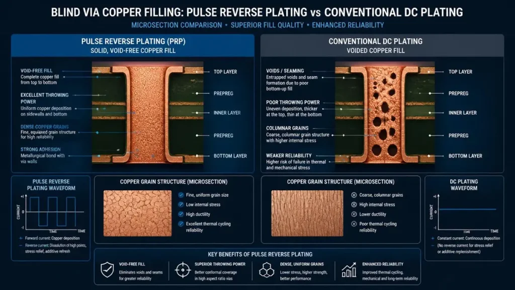
Microsection comparison between Pulse Reverse Plating (void-free copper filling, fine grain structure) and Conventional DC Plating (void defects, columnar grains) at Shenzhen Hongda Circuit Technology.
Copper filling is critical for via-in-pad (VIP) and stacked via reliability. Hongda Circuit employs:
- Vacuum-assisted filling: Removes trapped air before plating, reducing void content to <2%
- Pulse reverse plating: Produces equiaxed copper grain structures with 30% higher fatigue resistance than DC plating
- Leveling additives: Ensure surface planarity within 5μm for fine-pitch BGA assembly
- Thickness uniformity: ±10% across the entire panel, verified by eddy-current mapping
Sequential Lamination with Automated Alignment and Pressure Control
Our sequential lamination line features:
- Vacuum lamination presses: Eliminate air entrapment and ensure complete resin flow
- Programmable pressure profiles: Optimized for each material stack-up to prevent resin starvation
- Post-lamination X-ray alignment verification: Confirms layer-to-layer registration before drilling
- High-Tg material expertise: Processing Tg 180°C–200°C materials for automotive and aerospace
Advanced Desmear and Surface Preparation for Optimal Copper Adhesion
Laser drilling generates resin smear that must be completely removed before plating. Our process includes:
- Plasma desmear: Removes organic residue from high-Tg and polyimide materials
- Chemical desmear: Optimized permanganate process for standard FR-4
- Brown oxide treatment: Creates micro-roughened copper surfaces for enhanced adhesion
- Plasma activation: Prepares resin surfaces for electroless copper deposition
Automated Optical Inspection (AOI) and X-ray Alignment Systems
Quality is built through inspection, not inspection alone. Hongda Circuit integrates:
- 3D AOI: Detects surface defects, solder mask alignment, and pad geometry
- X-ray alignment verification: Validates blind via registration before outer layer processing
- Automated microsection sampling: Robotic sectioning and preparation for consistent results
- Statistical process control (SPC): Real-time monitoring of critical parameters with automatic alerts
Material Selection Expertise for High-Reliability Blind Via PCB
Material selection profoundly impacts blind via reliability. Hongda Circuit maintains inventory and expertise in:
- M9-grade laminates: For 224Gbps AI server applications (Df ≤ 0.0008 @10GHz)
- High-Tg FR-4 (Tg 180°C–200°C): For automotive under-hood applications
- Low-CTE materials: For aerospace thermal stability requirements
- Halogen-free laminates: For environmentally conscious and medical applications
- Polyimide flex materials: For rigid-flex HDI constructions
Common Blind Via Reliability Problems and Engineering Solutions
Why Do Blind Vias Crack After Thermal Cycling?
Root cause: CTE mismatch between copper and laminate generates cyclical shear stress. Columnar grain structures in the copper barrel provide preferential crack paths.
Hongda Circuit solution:
- Pulse reverse plating to produce equiaxed grains
- Aspect ratio control below 0.8:1
- Optimized desmear for maximum copper-resin adhesion
- Thermal cycle correlation data for every material combination
Why Does Copper Separate from the Via Wall?
Root cause: Inadequate desmear or contamination prevents proper electroless copper adhesion. Oxidation of the landing pad before plating is another common cause.
Hongda Circuit solution:
- Dual-stage plasma + chemical desmear
- Controlled atmosphere between desmear and plating
- Automated copper thickness verification at 100% of vias
Why Does Resin Recede from Blind Via Barrels?
Root cause: Thermal aging embrittles high-Tg resins, causing them to pull away from the copper barrel during thermal cycling.
Hongda Circuit solution:
- Material pre-qualification with thermal cycling
- Optimized cure cycles for complete resin polymerization
- Low-stress resin systems for high-reliability applications
How Can CAF Be Prevented in Dense Blind Via Arrays?
Root cause: Moisture + ionic contamination + electric field = electrochemical migration along glass fibers.
Hongda Circuit solution:
- Low-CTE glass styles (106, 1080) with reduced glass content
- Strict ionic cleanliness controls (<1.0μg NaCl eq/cm²)
- Conformal coating options for high-humidity environments
- Design rule checks for minimum via spacing based on voltage
How to Improve Blind Via Filling Quality?
Root cause: Trapped air, insufficient plating agitation, or incorrect current density.
Hongda Circuit solution:
- Vacuum pre-treatment before filling
- Programmable pulse plating with optimized duty cycles
- Real-time void monitoring via X-ray inspection
- Process validation with cross-section analysis
How to Choose a Reliable Blind Via PCB Manufacturer: Procurement Guide and Supplier Checklist
Essential Equipment and Technology Requirements
| Capability | Minimum Requirement | Hongda Circuit Specification |
|---|---|---|
| Laser drilling | CO2 laser, 100μm vias | UV+CO2 hybrid, 50μm vias |
| Registration accuracy | ±25μm | ±10μm with drift compensation |
| Copper filling | DC plating | Pulse reverse with vacuum assist |
| Layer count | 12 layers | 40+ layers, 6+N+6 HDI |
| Line width/space | 75μm/75μm | 30μm/30μm production capability |
| X-ray inspection | 2D X-ray | 2D + 3D CT, 5μm resolution |
| Thermal testing | External lab | In-house thermal cycling + IST |
Certifications and Quality Systems to Verify
- ISO 9001: Quality management system (mandatory)
- IATF 16949: Automotive quality (for automotive suppliers)
- ISO 13485: Medical device quality (for medical applications)
- IPC-A-600: PCB acceptability standard
- UL certification: Product safety and flammability
- ITAR registration: For US defense applications
Reliability Reports and Documentation to Request
Before placing a production order, request:
- Thermal cycling report: Minimum 500 cycles with resistance data
- IST report: 200+ cycles with Weibull analysis
- Cross-section photos: Showing copper thickness, void content, and interface quality
- X-ray void analysis: Statistical data on void percentage distribution
- Material certifications: Including Tg, Td, CTE, and Df/Dk values
- Process capability study: Cpk values for critical parameters
- Customer reference list: Similar applications and volumes
Engineering Support and DFM Review Capability
A reliable blind via manufacturer should provide:
- Pre-production DFM review: Identifying potential reliability risks before fabrication
- Stack-up optimization: Recommending materials and constructions for your application
- Test coupon design: Ensuring qualification coupons represent production boards
- Failure analysis support: Root cause analysis for any field failures
- Continuous improvement: Process updates based on latest industry learnings
Supplier Evaluation Scorecard for Blind Via PCB Procurement
| Evaluation Category | Weight | Scoring Criteria (1–5) |
|---|---|---|
| Technical capability | 25% | Equipment, layer count, precision |
| Quality certifications | 20% | ISO, IATF, IPC, UL |
| Reliability testing | 20% | In-house IST, thermal cycling, X-ray |
| Engineering support | 15% | DFM, stack-up, failure analysis |
| Track record | 10% | Years in business, customer references |
| Pricing and lead time | 10% | Competitiveness and flexibility |
Case Study — AI Server Microvia Crack Root Cause Analysis and Process Optimization
Problem Description: Microvia Failure in 500-Thermal-Cycle Qualification
A customer designing a 28-layer AI server backplane experienced microvia corner cracks after 500 thermal cycles (-40°C to +125°C). The design used 2+N+2 HDI construction with 100μm blind vias on 250μm pitch.
Failure Analysis Methodology
Hongda Circuit’s failure analysis team performed:
- Electrical characterization: Resistance increase of 15% at 500 cycles, catastrophic open at 650 cycles
- X-ray inspection: No visible voids; alignment within specification
- Cross-section analysis: Crack initiation at via corner, propagation through barrel wall
- SEM/EDX analysis: Columnar grain structure in copper barrel; sulfur contamination at crack interface
- Process audit: Identified insufficient pulse reverse plating duty cycle
Root Cause and Corrective Actions
Root cause: The pulse reverse plating parameters were optimized for throughput rather than grain structure, producing columnar grains that provided crack propagation paths.
Corrective actions:
- Revised pulse reverse waveform: 10ms forward, 2ms reverse, optimized peak current density
- Implemented grain structure verification via SEM on every qualification build
- Added thermal cycle correlation testing for new material combinations
- Updated process control limits with SPC monitoring
Results: Retest coupons achieved 1500+ cycles with <3% resistance drift. Customer approved for production.
Frequently Asked Questions (FAQ) — Blind Via PCB Reliability for Procurement Professionals
What Is Blind Via Reliability and Why Does It Matter for My Application?
Blind via reliability is the ability of a buried interconnect to maintain electrical and mechanical integrity throughout the product’s service life under all specified environmental conditions. It matters because blind via failure is the dominant failure mode in HDI PCBs—studies show that 60–70% of HDI field failures originate at via structures. For procurement, specifying and verifying blind via reliability protects your brand reputation, reduces warranty costs, and ensures supply chain continuity.
How Is Blind Via Reliability Tested and What Reports Should I Request?
Blind via reliability is tested through a combination of electrical, thermal, and mechanical methods. The core tests are:
Thermal cycling (-55°C to +125°C, 500–2000 cycles)
IST (Interconnect Stress Test, 200–300 cycles)
Cross-section analysis (copper thickness, voids, cracks)
X-ray inspection (void content, alignment)
Request complete test reports with raw data, statistical analysis, and photographic documentation. A reputable supplier like Hongda Circuit provides these as standard with every qualification build.
What Causes Blind Via Cracking and How Can Manufacturers Prevent It?
Blind via cracking is caused by the cumulative effect of CTE mismatch between copper and laminate during thermal cycling. Prevention strategies include:
Optimized aspect ratios: Keep depth-to-diameter below 0.8:1
Equiaxed copper grain structure: Achieved through pulse reverse plating
Thick copper barrels: Minimum 20μm, preferably 25–30μm
Proper desmear: Ensures strong copper-resin adhesion
Material selection: Match CTE properties to the application
What Is the IST Test for PCB and Is It Mandatory for Automotive Applications?
IST (Interconnect Stress Test) is an accelerated reliability test that subjects PCB interconnects to rapid thermal cycling via resistive self-heating. It is mandatory for automotive PCB suppliers under IATF 16949 and strongly recommended for telecom, medical, and aerospace applications. IST provides faster qualification than conventional thermal cycling (days vs. weeks) and correlates well with field reliability data.
Is Thermal Cycling Mandatory for All Blind Via PCB Applications?
Thermal cycling is mandatory for any application where the PCB will experience temperature variation during operation or storage. This includes virtually all applications except climate-controlled consumer electronics. The number of cycles and temperature range vary by industry:
Consumer: 250–500 cycles (0°C to +100°C)
Automotive: 1000–2000 cycles (-55°C to +150°C)
Aerospace: 2000+ cycles (-65°C to +150°C)
Building Blind Via Reliability from the Ground Up
Blind via reliability is not a single test or inspection—it is the cumulative result of intelligent design, advanced manufacturing, rigorous testing, and continuous improvement. In 2026, as AI servers push data rates beyond 200Gbps, as autonomous vehicles demand 15-year lifespans, and as medical devices become permanently implanted, the stakes for blind via reliability have never been higher.
At Shenzhen Hongda Circuit Technology Co., Ltd., we have built our reputation on delivering blind via PCBs that exceed industry standards. Our investment in femtosecond laser technology, pulse reverse plating, vacuum-assisted filling, and comprehensive in-house testing ensures that every blind via we produce is engineered for reliability from the first laser pulse to the final cross-section.
Whether you are qualifying a supplier for your next AI accelerator, automotive ECU, or medical implant, we invite you to experience the Hongda Circuit difference. Contact our engineering team for a detailed DFM review, reliability qualification plan, or factory tour.
About Shenzhen Hongda Circuit Technology Co., Ltd.
Shenzhen Hongda Circuit Technology Co., Ltd. is a leading HDI PCB manufacturer specializing in high-reliability blind via technology for AI servers, automotive electronics, medical devices, and aerospace applications. With ISO 9001, IATF 16949, and ISO 13485 certifications, Hongda Circuit delivers precision-manufactured PCBs with industry-leading reliability performance.
Contact: pcb@pcbkr.com Website: www.pcbkr.com Certifications: ISO 9001 | IATF 16949 | ISO 13485 | IPC-A-600 Class 3 | UL
About Author
David Chen https://www.linkedin.com/in/pcbcoming
David Chen boasts an extensive professional background in PCBA manufacturing, PCBA testing, and PCBA optimization, with specialized expertise in high-precision PCBA fault analysis and rigorous PCBA reliability testing. The author has worked with high-layer-count server PCB fabrication, ultra-low-loss backplane stackups, and thermo-mechanical reliability optimization for AI infrastructure projects involving 112G and 224G PAM4 architectures. Skilled in complex circuit design and cutting-edge advanced PCB manufacturing processes, he delivers solutions that elevate product durability and performance across industrial applications. His technical articles focusing on PCBA manufacturing workflows and testing methodologies are widely cited by industry peers, research institutions, and technical platforms, solidifying his reputation as a recognized technical authority in the global circuit board manufacturing sector.