LED PCB Solutions: The Definitive B2B Guide to LED Circuit Board Design, Manufacturing, and Procurement
Every LED lighting system—whether it is a high-bay industrial fixture, an automotive headlight module, or a fine-pitch indoor display—depends on one component that most end users never see: the LED PCB. Also referred to as an LED circuit board or LED PCB board, this substrate is not merely a mounting platform for diodes. It is the primary thermal pathway, the electrical distribution network, and the mechanical foundation that determines whether an LED product lasts 50,000 hours or fails within six months.
At Shenzhen Hongda Circuit Technology Co., Ltd. , we have spent over a decade manufacturing high-precision PCB LED solutions for global markets spanning 5G-Advanced infrastructure, semiconductor test equipment, automotive Tier-1 supply chains, and commercial lighting OEMs. We have seen procurement teams repeatedly struggle with the same set of problems: thermal runaway in aluminum substrates, inconsistent solder joint quality in SMD LED PCB assemblies, and prototype-to-production mismatches that derail product launches. This guide was written to eliminate those blind spots.
If you are a purchasing manager, an engineering buyer, or a product manager evaluating custom LED PCB suppliers, the sections below will walk you through material selection, thermal design, manufacturing processes, and the exact criteria you should use to qualify a factory. We have structured this content around the real questions buyers type into Google—“how to design LED PCB,” “aluminum LED PCB vs FR4,” and “LED PCB assembly turnaround time”—because your procurement decisions should be grounded in verifiable engineering data, not marketing claims.
What Is an LED PCB? Understanding the Circuit Board Behind Every Lighting System
An LED PCB is a printed circuit board specifically engineered to mount light-emitting diodes, route electrical current, and—most importantly—dissipate the heat those diodes generate. Unlike standard signal boards, an LED circuit board operates under a thermal load that can exceed 1 W/cm² in high-power arrays. If that heat is not conducted away from the LED junction, lumen depreciation accelerates, color shift occurs, and catastrophic solder joint failure becomes inevitable.
The Anatomy of an LED Circuit Board: Copper, Dielectric, and Substrate
Every LED PCB board consists of three functional layers, even if the materials vary:
- Circuit Layer (Top Copper): Typically 1 oz to 3 oz (35–105 µm) thick, this layer carries current to the LED pads. In power LED PCB designs, copper weight is increased to 4 oz or 6 oz to reduce resistive heating and voltage drop across long traces.
- Dielectric Layer: In a metal core PCB LED, this is a thermally conductive but electrically isolating material—often an epoxy-based prepreg with ceramic fillers. Thermal conductivity here ranges from 1.0 W/m·K to 4.0 W/m·K, and thickness is usually 75–150 µm. The dielectric is the thermal bottleneck of the entire stack-up; a thinner, higher-conductivity dielectric improves heat transfer but reduces dielectric strength.
- Base Substrate: In standard FR4 LED PCB boards, this is woven glass-reinforced epoxy. In aluminum LED PCB constructions, it is an aluminum alloy (1050 or 1060 series) with a thermal conductivity of roughly 180 W/m·K. For extreme applications, ceramic substrates such as aluminum nitride (AlN) reach 170–200 W/m·K.
The thermal resistance of the entire stack—from LED junction to ambient air—is the metric that matters. A poorly designed LED light PCB board can have a junction temperature 40°C higher than an optimized one, cutting LED life in half.
Why Thermal Management Is the Single Most Critical Factor in LED PCB Performance
LEDs convert only 30–40% of input energy into visible light; the remainder becomes heat. In a high power LED PCB, that waste energy must travel through the dielectric, spread across the metal base, and exit into a heat sink or ambient air. If any layer in that chain underperforms, the junction temperature (Tj) climbs above the manufacturer’s rated maximum—usually 125°C or 150°C—and luminous efficacy collapses.
In 2026, the industry is witnessing a decisive shift toward metal core PCB LED substrates for any application above 0.5 W per LED. FR4, with a thermal conductivity of only 0.3–0.4 W/m·K, simply cannot move heat fast enough for modern high-brightness chips. Buyers who still specify FR4 for mid-power arrays are paying for premature field failures. The math is unforgiving: for every 10°C rise above rated Tj, LED lifetime degrades by approximately 50%. A board running 30°C hot fails eight times faster than one operating within specification.
Types of LED PCB Boards: From Standard FR4 to Metal Core and Ceramic Substrates
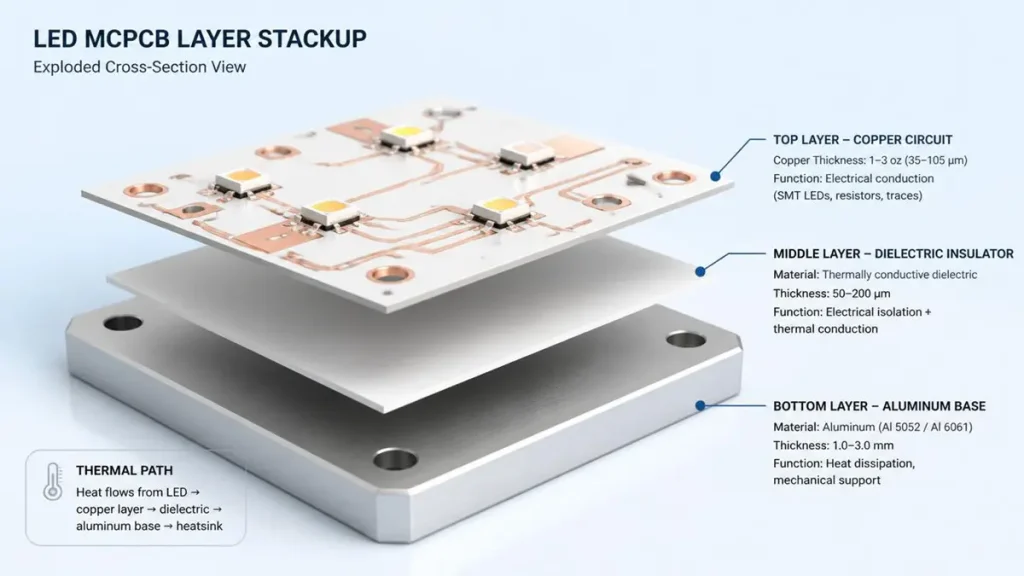
Exploded view of a single-layer Aluminum MCPCB stackup showing thermal path and functional layers.
Not every lighting application demands the same substrate. A decorative indoor fixture has radically different thermal and mechanical requirements than an EV charging station indicator or a stadium floodlight. Understanding the trade-offs between substrate types is the first step in LED PCB board design that does not fail in the field.
FR4 LED PCB Boards: When Low Cost Outweighs Thermal Performance
FR4 remains viable for low-power indicator LEDs, battery-operated devices, and short-life consumer products. In these cases, thermal vias can partially compensate for FR4’s poor conductivity by creating vertical copper paths to a bottom-side copper pour. However, for arrays exceeding 10 W total dissipation, FR4 becomes a liability. The thermal vias add manufacturing cost, the board warps under thermal cycling, and the overall system reliability drops.
From a procurement standpoint, FR4 LED PCB boards are attractive only when the Bill of Materials (BOM) cost is the dominant constraint and product lifespan is secondary. For anything destined for commercial, industrial, or outdoor environments, FR4 should be viewed as a false economy. We have replaced too many failed FR4 boards for customers who initially chose price over performance.
Aluminum LED PCB (MCPCB): The Industry Standard for High-Power LED Applications
The aluminum LED PCB, technically a Metal Core Printed Circuit Board (MCPCB), has become the default choice for street lighting, downlights, high-bay fixtures, and automotive exterior lamps. The aluminum base acts as both a structural plate and a heat spreader, eliminating the need for a separate metal backing in many designs.
At Hongda Circuit, our LED PCB manufacturing lines process aluminum substrates up to 3.0 mm thick, with dielectric thermal conductivity options of 1.5 W/m·K, 2.2 W/m·K, and 3.0 W/m·K. We typically recommend the 2.2 W/m·K grade for outdoor LED street light PCB applications, because it strikes the optimal balance between thermal performance and dielectric withstand voltage. For indoor commercial lighting where space is constrained, the 3.0 W/m·K grade allows thinner boards without sacrificing heat dissipation.
Advanced Ceramic LED PCBs: Aluminum Nitride for Extreme Thermal Loads
For UV-C sterilization LEDs, laser diode modules, and high-density COB arrays where junction temperatures exceed 150°C, ceramic substrates enter the conversation. Aluminum nitride (AlN) offers thermal conductivity of 170–200 W/m·K and a coefficient of thermal expansion (CTE) closely matched to silicon. The trade-off is cost: AlN substrates can be 5× to 10× more expensive than aluminum MCPCB. Procurement teams should reserve ceramic PCB LED solutions for applications where failure is not an option—medical devices, aerospace lighting, and high-power industrial curing systems.
Aluminum LED PCB vs. FR4 PCB: A Procurement Engineer’s Decision Matrix
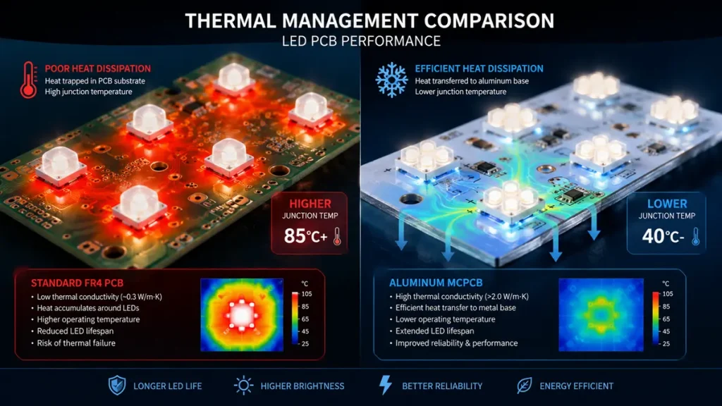
Thermal dissipation comparison between standard FR4 PCB (left) and aluminum MCPCB (right), demonstrating lower junction temperatures and efficient thermal transfer.
The LED PCB vs standard PCB debate is not about which material is “better.” It is about matching substrate properties to operational reality. We have compiled the decision criteria we use when consulting buyers at the quotation stage:
| Parameter | FR4 LED PCB Board | Aluminum LED PCB (MCPCB) | Ceramic LED PCB (AlN) |
|---|---|---|---|
| Thermal Conductivity | 0.3–0.4 W/m·K | 1.0–5.0 W/m·K (dielectric) / 180 W/m·K (base) | 170–200 W/m·K |
| Typical Copper Weight | 1–2 oz | 1–6 oz | Thick film / DPC / DBC |
| Max LED Power Density | < 0.3 W/cm² | Up to 2.5 W/cm² | > 5 W/cm² |
| Relative Cost | Low | Medium | High |
| Typical Applications | Indicators, toys, low-power decorative | Street lights, downlights, automotive, displays | UV LEDs, lasers, medical, military |
| Mechanical Rigidity | Moderate | High | Very High (brittle) |
Buyers evaluating custom LED PCB quotations should demand that suppliers disclose the exact dielectric material and thermal conductivity rating. A supplier quoting an “aluminum PCB” without specifying dielectric performance is leaving thermal performance to chance. We have seen competitors quote 0.8 W/m·K dielectrics at prices that seem attractive—until the customer discovers their street lights are failing after 8,000 hours instead of 50,000.
Power LED PCB Design: Managing Voltage, Current Density, and Heat Dissipation
Once the substrate is selected, the electrical design determines whether the power LED PCB operates within its thermal envelope or drifts into failure. This is where many procurement disputes originate: a buyer orders 1,000 boards based on a prototype that worked, only to discover that the production batch has different copper weights, trace geometries, or solder mask coverage that push junction temperatures over the limit.
220V LED PCB Direct-Drive Architectures vs. Constant-Current Driver Designs
In markets such as Turkey and parts of Southeast Asia, 220V LED PCB direct-drive designs are common for cost-sensitive bulb and panel applications. These boards integrate a bridge rectifier and a current-limiting resistor directly on the PCB, eliminating the external driver. The advantage is BOM cost reduction. The risk is that any fluctuation in mains voltage translates directly into LED current variation, accelerating lumen depreciation.
For commercial and industrial buyers, we strongly recommend discrete constant-current driver ICs mounted on the LED PCB board or housed in a separate driver enclosure. The additional $0.50–$1.20 per fixture pays for itself in extended LED life and stable color temperature. At Hongda Circuit, our LED PCB design team can review your schematic to determine whether a direct-drive or driver-on-board architecture is appropriate for your target market’s voltage stability and safety regulations.
Copper Weight Selection for High-Current LED PCB Boards
Trace heating is often underestimated in LED PCB board design. A 1-oz copper trace carrying 1 A over a 50 mm length will experience a temperature rise of approximately 10°C. In a multi-LED array where cumulative current reaches 5 A or more, 1-oz copper becomes a heating element rather than a conductor.
Our standard recommendation for high power LED PCB arrays is 2-oz minimum copper, with 3-oz or 4-oz for series strings exceeding 3 A. For automotive headlight modules and EV charging indicators, we routinely fabricate 6-oz copper on aluminum substrates, using etch compensation to maintain trace width accuracy despite the increased copper thickness. The rule of thumb: if your trace is getting warm during bench testing, your copper is too thin for production.
Thermal Via Arrays and Heat Sink Integration Strategies
Even with an aluminum base, localized hotspots can form under high-density COB LEDs. Thermal vias—plated through-holes filled with thermally conductive epoxy—create vertical heat pipes from the top copper layer directly to the metal substrate. In a well-designed metal core PCB LED, thermal vias under each LED pad can reduce thermal resistance by 15–30%.
The placement pattern matters. A grid of 0.3 mm vias on 0.8 mm pitch under the LED thermal pad is standard for mid-power chips. For COB modules, we recommend a solid copper slug or direct die-attach to ceramic rather than relying solely on vias. When Hongda Circuit engineers review a LED PCB design for DFM (Design for Manufacturability), thermal via density and proximity to solder mask openings are among the first items we flag. A common error is placing thermal vias too close to the pad edge, where solder wicking during reflow can create voids or starve the joint.
SMD LED PCB Assembly: Integrating 3535, 5050, 5054, and COB LED Modules

High-speed SMT assembly line placing precision components on LED circuit boards.
Surface-mount device (SMD) LEDs dominate the commercial lighting market because they enable automated assembly, high packing density, and consistent optical performance. However, SMD LED PCB assembly is not simply standard PCBA with brighter components. The thermal profile, solder paste selection, and inspection criteria are all specialized.
Reflow Soldering Profiles for SMD LED PCB Manufacturing
LED packages—whether 3528, 3535 LED PCB modules, 5050 RGB, or 5054 high-power—are sensitive to peak reflow temperature. Exceeding 260°C for more than a few seconds can degrade the phosphor coating, shift color coordinates, or damage the internal wire bond. At the same time, insufficient peak temperature or too-short time-above-liquidus (TAL) produces cold solder joints that fail under thermal cycling.
Our SMT lines at Shenzhen Hongda Circuit Technology use SAC305 lead-free solder paste with a peak reflow temperature of 245–250°C and a TAL of 60–90 seconds. For CREE LED PCB modules and other premium chips with strict manufacturer profiles, we program oven zones individually and attach thermocouples to test boards for thermal profiling verification. Buyers should never accept a PCBA supplier who cannot provide a reflow profile chart specific to their LED part number. That chart is your insurance policy against field failures.
AOI and X-Ray Inspection Protocols for LED PCBA Quality Assurance
After reflow, every LED PCB assembly undergoes Automated Optical Inspection (AOI) to detect tombstoning, solder bridging, and missing components. For boards with bottom-terminated components or thermal vias that must remain fully filled, we add X-Ray inspection to verify void content. IPC-A-610 Class 2 standards permit up to 25% voiding in thermal vias; for automotive LED PCB applications, we enforce Class 3 criteria with voiding below 10%.
In 2026, AI-driven AOI systems are becoming standard in advanced factories. At Hongda Circuit, we have integrated machine-learning defect classification that reduces false-call rates by 40% compared to rule-based AOI, ensuring that genuine solder defects are caught without wasting engineering time on phantom rejections. This matters when you are building 10,000 street light modules and cannot afford a 2% field failure rate.
Industry-Specific LED PCB Applications and Compliance Requirements
Different vertical markets impose different mechanical, thermal, and regulatory constraints on LED circuit board design. A board that works perfectly in a warehouse high-bay may fail catastrophically under the hood of a vehicle. Understanding these differences before you issue a purchase order saves months of redesign.
LED Street Light PCB: IP65-Rated MCPCB for Outdoor Luminaires
The LED street light PCB is one of the most thermally demanding applications in commercial lighting. A 150 W street lamp may contain 100+ high-power LEDs dissipating heat into a sealed IP65 housing with minimal air circulation. The LED PCB board must therefore conduct heat not just to a heat sink, but through the entire luminaire body.
At Hongda Circuit, we have supplied LED street light PCB boards to municipal retrofit projects across South Asia and the Middle East. Our standard specification for these applications is a 2.0 mm aluminum substrate with 2-oz copper and a white solder mask to maximize reflectivity. We also offer conformal coating as an add-on service for boards operating in coastal or high-humidity environments where salt spray accelerates corrosion. One lesson we learned from field returns: always specify a dielectric breakdown voltage above 3 kV for outdoor boards. The 2.0 kV grade fails within two years in tropical climates due to moisture ingress.
Automotive LED PCB: AEC-Q200 and IATF 16949 Standards for Vehicle Lighting
Automotive lighting—headlights, taillights, daytime running lamps, and interior ambient lighting—subjects automotive LED PCB boards to vibration, thermal shock, and electromagnetic interference. Suppliers to this market must demonstrate compliance with AEC-Q200 for passive components and operate under IATF 16949 quality management systems.
Our Shenzhen facility is IATF 16949 certified, and we routinely produce automotive LED PCB boards with high-TG dielectrics, ENIG surface finish for wire-bonding compatibility, and 100% electrical testing. For headlight modules, we can fabricate double-sided aluminum PCBs with blind vias to accommodate complex driver circuits on the same board as the LED array. The automotive procurement cycle is long—typically 18–24 months from RFQ to SOP—so choosing a supplier with proven PPAP (Production Part Approval Process) capability is essential.
LED Display PCB and RGB Pixel Board Design for Commercial Screens
Indoor and outdoor LED displays rely on RGB LED PCB boards with tightly controlled pixel pitch. A P2.5 indoor screen requires SMD 2121 or 1515 LEDs on a LED display PCB with trace geometries accurate to ±0.02 mm. Any variation in trace length between the red, green, and blue channels creates color imbalance at the module edge.
Hongda Circuit manufactures LED display PCB boards up to 6 layers with impedance-controlled RGB lines and black solder mask to improve contrast ratio. For outdoor rental displays, we specify 1.6 mm FR4 or aluminum substrates with gold-plated edge connectors rated for 500+ insertion cycles. The 2026 trend toward COB (Chip-on-Board) display modules is pushing us to develop direct-mount ceramic substrates for fine-pitch applications where SMD packages are reaching their size limit.
The LED PCB Manufacturing Process: From Gerber Files to Finished Boards
Understanding how an LED PCB is fabricated helps buyers ask better questions during supplier audits. The process for an aluminum LED circuit board differs significantly from standard FR4 fabrication in several critical steps.
Substrate Preparation and Thermal Adhesive Lamination
Aluminum panels arrive from the mill with a protective film and surface oxidation. The first step is alkaline degreasing and micro-etching to create a fresh surface for lamination. The copper foil and dielectric prepreg are then bonded to the aluminum base in a vacuum hot press at 120–160°C. Pressure uniformity is critical; any air pocket or resin-starved area becomes a thermal void that concentrates heat.
At Hongda Circuit, we inspect every laminated panel with ultrasonic scanning before etching. Panels exhibiting delamination or dielectric thickness variation outside ±10 µm are rejected. This upstream quality control is why our field-failure rate for LED PCB boards remains below 0.3% across all product lines. We would rather scrap a $20 panel than ship a board that fails in a customer’s end product.
Circuit Pattern Etching and CNC Drilling for LED PCB Fabrication
After lamination, the copper layer is patterned using dry-film photoresist and alkaline etching. For high power LED PCB designs with 4-oz or 6-oz copper, etch undercut becomes significant. We compensate trace widths by 0.05–0.10 mm per side, depending on copper weight, to ensure final geometries meet the Gerber specification.
Drilling is performed on CNC machines with ±0.05 mm positional accuracy. For LED PCB prototype runs, we use laser drilling for microvias as small as 0.10 mm, enabling high-density interconnect (HDI) designs that would be impossible with mechanical drills. Our 120+ layer backplane capability—originally developed for 5G infrastructure—gives us the precision equipment needed for demanding LED applications.
Surface Finish Selection: ENIG, OSP, or HASL for LED Applications
The surface finish determines solderability, wire-bondability, and long-term corrosion resistance:
- ENIG (Electroless Nickel Immersion Gold): The default for SMD LED PCB applications. It provides flat, oxidation-resistant pads with excellent solder joint reliability. We recommend ENIG for any board using SAC305 lead-free solder. Typical thickness: 3–5 µm nickel, 0.05–0.10 µm gold.
- OSP (Organic Solderability Preservative): Lower cost than ENIG and suitable for single-sided aluminum boards with short shelf-life requirements. OSP is less reliable for double-reflow processes and is not recommended for boards stored longer than six months before assembly.
- HASL (Hot Air Solder Leveling): Rarely used for LED applications because the uneven surface can cause component tilting and inconsistent thermal contact in COB modules. We only recommend HASL for through-hole prototypes where cost is the absolute priority.
How to Choose a Reliable LED PCB Manufacturer: A Buyer’s Technical Checklist
Selecting a LED PCB manufacturer China or any global supplier requires more than comparing unit prices. The buyers who avoid supply-chain disasters are the ones who verify capabilities before placing the purchase order. After fifteen years in this industry, we have identified the six questions that separate professional suppliers from trading companies posing as factories.
Certifications That Matter: ISO 9001, UL, RoHS, and IPC-A-610
At minimum, your supplier should hold ISO 9001:2015 for quality management. If you are selling into North America, UL listing (UL 796 for PCBs, UL 94 for flammability) is often mandatory for insurance and code compliance. RoHS and REACH compliance are non-negotiable for EU markets. For automotive LED PCB projects, demand IATF 16949 and IPC-A-610 Class 3 acceptance criteria.
Hongda Circuit maintains ISO 9001, ISO 14001, IATF 16949, and UL certifications. We provide full material declarations and third-party test reports on request. When a buyer asks for our ISO certificate and receives a PDF with a three-year-old date, that is a red flag. We update our documentation quarterly and make it available through our customer portal.
Prototype-to-Production Consistency: Why Your Sample Supplier Must Scale
A common procurement trap is qualifying a LED PCB prototype from a quick-turn shop, then transferring mass production to a lower-cost factory. The problem is that prototype shops often use different base materials, drill stacks, or etch chemistries than volume manufacturers. The result is a production batch with different thermal performance, color rendering, or mechanical dimensions than the approved sample.
We recommend choosing a supplier capable of both LED PCB prototype and volume production under the same process parameters. At Hongda Circuit, our prototype line uses the same lamination presses, etch lines, and AOI equipment as our volume lines. A board approved at 5 pieces will behave identically at 50,000 pieces. This is not marketing speak—it is process control. We run the same thermal profile, the same solder mask, and the same surface finish chemistry across all quantities.
Engineering Support: DFM Review and Thermal Simulation Capabilities
The best custom LED PCB suppliers do not just manufacture what you send them; they tell you what is wrong with it before fabrication. A DFM review should cover trace width adequacy, thermal via placement, solder mask clearance around LED pads, and panelization for assembly efficiency.
At Shenzhen Hongda Circuit Technology, our engineering team reviews every LED PCB design submission within 24 hours. We use thermal simulation software to estimate junction temperatures under rated current, and we flag designs that exceed safe operating limits before a single dollar is spent on tooling. In 2024 alone, our DFM reviews caught 47 designs with insufficient copper weight for their current load—saving our customers an estimated $180,000 in potential rework and field failures.
Custom LED PCB Services at Shenzhen Hongda Circuit Technology Co., Ltd.
Hongda Circuit is not a catalog vendor. We are a vertically integrated LED PCB manufacturer with fabrication, assembly, and design engineering under one roof in Shenzhen. Our capabilities reflect the demands of the markets we serve:
Rapid LED PCB Prototype Turnaround: From 24-Hour Samples to Volume Production
Our LED PCB prototype service delivers first-article aluminum boards in 24–72 hours for single-layer designs and 3–5 days for multilayer or HDI constructions. Every prototype includes a dimensional report, thermal conductivity certificate for the dielectric, and microsection photographs showing copper thickness and dielectric integrity.
For buyers evaluating multiple LED PCB board design iterations, we offer a structured NPI (New Product Introduction) program that includes design review, pilot builds, and process validation before mass production commitment. This eliminates the “sample roulette” where buyers approve one board and receive something different in volume.
Turnkey LED PCB Assembly: SMT, DIP, and Full PCBA Under One Roof
Beyond bare-board fabrication, Hongda Circuit operates six SMT lines with Yamaha high-speed pick-and-place equipment capable of placing 01005 components at ±0.035 mm accuracy. Our LED PCB assembly services include solder paste printing, reflow, AOI, X-Ray, functional testing, and conformal coating.
For buyers sourcing LED light PCB board modules complete with LEDs, drivers, and connectors, our turnkey PCBA service eliminates the coordination overhead of managing multiple vendors. We source components through authorized channels, manage BOM revisions, and deliver finished, tested modules ready for final assembly. One invoice, one point of contact, one quality standard.
Global Supply Chain Support for 5G, Automotive, and Industrial LED Markets
Our customer base spans telecommunications infrastructure, automotive Tier-1 suppliers, and industrial automation OEMs. This diversity has forced us to maintain quality systems and material traceability standards that exceed typical commercial LED PCB manufacturing shops. Whether you need a 1-layer aluminum LED PCB for a residential downlight or a 12-layer HDI board for a 5G base station with integrated status LEDs, the same quality system governs both.
We ship to North America, Europe, the Middle East, and Southeast Asia weekly. Our logistics team handles customs documentation, HS code classification, and Incoterms negotiation so your procurement team can focus on product development rather than freight forwarding.
LED PCB Design Guidelines: Layout, Copper Weight, and Heat Sink Integration
For buyers who handle LED PCB board design in-house, the following guidelines will prevent the most common design errors we encounter during DFM review:
- Keep LED thermal pads centered over the aluminum base: Offsetting the LED array toward the board edge creates asymmetric heat spreading and warping during reflow. Centering the heat source ensures even thermal distribution across the metal core.
- Use thermal relief patterns for large copper pours: Solid copper planes connected directly to small pads act as heat sinks during hand soldering, making rework difficult. Thermal relief spokes (0.3 mm wide, 4 spokes) improve solderability without compromising thermal performance.
- Maintain 0.25 mm solder mask clearance around LED pads: Insufficient clearance causes solder mask encroachment onto the pad, reducing wetting area and creating voids. We have seen assemblies with 40% voiding simply because the solder mask opening was too tight.
- Specify white solder mask for reflective applications: White solder mask reflects up to 85% of visible light, improving luminaire efficacy. Black or matte green masks absorb light and reduce system efficiency by 5–10%. For display applications, use black solder mask to improve contrast.
- Panelize with V-scoring for aluminum boards under 1.0 mm: Aluminum substrates cannot be routed with standard PCB routing bits without burr formation. V-scoring or jump-scoring is the preferred depanelization method for thin aluminum LED PCB boards. Thicker boards (2.0 mm+) can be routed with specialized tooling.
- Account for CTE mismatch in multilayer designs: Aluminum expands at 23 ppm/°C while FR4 expands at 14–17 ppm/°C. In hybrid constructions, this differential causes delamination under thermal cycling. Use high-TG dielectrics with matched CTE or avoid hybrid stack-ups entirely.
FAQ: LED PCB Procurement Questions Buyers Ask on Google
What is the difference between an LED PCB and a standard PCB?
An LED PCB is optimized for thermal dissipation and high-current trace capacity, whereas a standard PCB prioritizes signal integrity and cost. LED circuit boards typically use aluminum or ceramic substrates with thermally conductive dielectrics, while standard PCBs use FR4. If you install high-power LEDs on a standard FR4 board without thermal vias or metal backing, junction temperatures will exceed safe limits and the LEDs will degrade prematurely. The fundamental difference is that an LED PCB is a thermal management device first and an electrical circuit second.
How do I choose between aluminum LED PCB and FR4 for my lighting project?
Choose an aluminum LED PCB (MCPCB) when your LED array exceeds 0.5 W per chip or 10 W total board dissipation. Choose FR4 only for low-power indicators, battery devices, or cost-driven disposable products. The decision matrix is simple: if the product must last more than three years in continuous operation, aluminum is the safer procurement choice. Always request the dielectric thermal conductivity rating from your supplier; values below 1.0 W/m·K are insufficient for modern high-brightness LEDs. Also verify that the supplier uses ultrasonic scanning to detect delamination before etching.
What files does a LED PCB manufacturer need to start production?
For custom LED PCB manufacturing, you need Gerber files (RS-274X format), a drill file, a pick-and-place file if you require assembly, and a BOM for turnkey LED PCB assembly. Additionally, provide a fabrication drawing specifying substrate material, copper weight, surface finish, solder mask color, and any impedance or thermal requirements. At Hongda Circuit, our engineers can also work from Altium, Eagle, or KiCad source files if Gerbers are not yet finalized. The more detail you provide in the fabrication notes—especially thermal requirements and expected operating temperatures—the more accurate our DFM review will be.
How long does LED PCB prototype and mass production take?
Single-layer LED PCB prototype turnaround is typically 24–72 hours at Hongda Circuit. Double-sided aluminum or multilayer boards require 3–5 days. Mass production lead times range from 7 days for 1,000 pieces to 15–20 days for 10,000+ pieces, depending on substrate availability and SMT complexity. For urgent projects, we maintain buffer stock of common aluminum substrate thicknesses (1.0 mm, 1.5 mm, 2.0 mm) to compress procurement cycles. If you are facing a trade-show deadline or a customer pilot program, tell us upfront. We have expedited prototypes to 12 hours for customers with genuine emergencies.
Why do LED PCBs fail prematurely, and how do I prevent it?
Premature LED PCB board failure almost always traces back to one of three root causes: inadequate thermal management (wrong substrate or missing heat sink), solder joint fatigue from thermal cycling (often due to incorrect reflow profile or CTE mismatch), or electrical overstress from poorly designed current-limiting circuits. Prevention starts at the design stage: specify the correct substrate for your thermal load, demand reflow profile verification from your PCBA supplier, and include transient voltage suppression if your application experiences mains voltage spikes. Finally, always run an 85°C/85% RH humidity test for 1,000 hours on your prototype before approving mass production. Boards that survive this test rarely fail in the field.
Conclusion: Building Your Next LED PCB Project with Confidence
The LED PCB market in 2026 is defined by two opposing forces: relentless cost pressure from commoditized lighting products, and escalating performance demands from automotive, display, and industrial applications. Buyers who treat the LED circuit board as a commodity—shopping solely on price per square meter—inevitably face field failures, warranty claims, and supply-chain disruptions. Buyers who treat it as a thermal and electrical engineering component, demanding material traceability, DFM review, and process validation from their suppliers, build products that last.
At Shenzhen Hongda Circuit Technology Co., Ltd., we have built our operation around the second philosophy. From LED PCB prototype to mass production, from single-layer aluminum boards to multilayer HDI assemblies, every board is manufactured under the same quality system that serves our 5G and automotive customers. If you are evaluating suppliers for your next lighting project, send us your Gerber files or design requirements. Our engineering team will return a DFM report, thermal assessment, and quotation within one business day.
Ready to start your LED PCB project? Email sales@pcbkr.com or upload your files through our RFQ portal for an engineering review and competitive quotation.
About Author
David Chen https://www.linkedin.com/in/pcbcoming
David Chen boasts an extensive professional background in PCBA manufacturing, PCBA testing, and PCBA optimization, with specialized expertise in high-precision PCBA fault analysis and rigorous PCBA reliability testing. The author has worked with high-layer-count server PCB fabrication, ultra-low-loss backplane stackups, and thermo-mechanical reliability optimization for AI infrastructure projects involving 112G and 224G PAM4 architectures. Skilled in complex circuit design and cutting-edge advanced PCB manufacturing processes, he delivers solutions that elevate product durability and performance across industrial applications. His technical articles focusing on PCBA manufacturing workflows and testing methodologies are widely cited by industry peers, research institutions, and technical platforms, solidifying his reputation as a recognized technical authority in the global circuit board manufacturing sector.