Rogers High Frequency PCB Prototype: A Complete Guide to Fast-Turn Sourcing in 2026
The demand for high frequency PCB prototyping has never been sharper. From 5G base stations and millimeter-wave radar modules to AI server interconnects and satellite communication hardware, the modern electronics industry depends on materials that perform reliably at microwave and RF frequencies. In this environment, engineers and procurement managers cannot afford to wait weeks for a single prototype run.
At Shenzhen Hongda Circuit Technology Co., Ltd., we have spent years refining a manufacturing workflow that delivers every Rogers High Frequency PCB Prototype within 24 to 48 hours with no minimum order quantity. This guide explains how that is possible, what materials and processes are involved, and how to apply 2026’s latest PCB fabrication advances to your next RF or microwave design.
Why Rogers Material Remains the Gold Standard for RF and Microwave PCBs
Engineers who have worked with standard FR-4 laminate know its limitations at high frequencies: rising dielectric loss, inconsistent Dk values, and poor thermal management at elevated power levels. Rogers materials were engineered specifically to address these constraints.
1. Key Dielectric Properties That Define High-Frequency Performance
When selecting a laminate for RF or microwave applications, three parameters dominate the decision: dielectric constant (Dk), dissipation factor (Df), and coefficient of thermal expansion (CTE).
- Dk stability across temperature and frequency keeps impedance predictable from prototype to production
- Low dissipation factor (Low Df) minimizes insertion loss in transmission lines and antenna feed networks
- Matched CTE reduces mechanical stress at solder joints during thermal cycling
Rogers laminates such as RO4350B deliver a Dk of 3.48 ±0.05 and a Df of only 0.0037 at 10 GHz — figures that FR-4 simply cannot match. For engineers designing controlled impedance PCBs, that consistency is critical from the very first prototype.
2. Rogers Material vs FR-4: When to Make the Switch
| Parameter | Rogers RO4350B | Standard FR-4 |
| Dielectric Constant (Dk) | 3.48 ±0.05 @ 10 GHz | 4.2–4.8 (varies widely) |
| Dissipation Factor (Df) | 0.0037 @ 10 GHz | 0.020–0.025 |
| CTE (x/y axis) | 14 ppm/°C | 14–18 ppm/°C |
| Max Operating Temp | 280°C | 130°C |
| Signal Loss at 10 GHz | Very Low | High |
| Typical Application | RF, Microwave, 5G, Radar | Digital, low-frequency |
Rogers PCB Material Inventory: Fast-Turn Availability in 2026
One of the most common causes of prototype delays is material procurement. Standard Rogers laminates carry lead times of one to three weeks when ordered on demand. Hongda eliminates this bottleneck by maintaining on-shelf inventory of the most specified Rogers grades.
1. RO4350B PCB — The Industry Workhorse
Rogers 4350B remains the single most ordered substrate in our facility. Its combination of low Df, UL 94 V-0 flame rating, and compatibility with standard FR-4 processing chemistry makes it the default choice for RF modules, 5G antenna arrays, and power amplifier boards. We stock multiple thicknesses from 0.254 mm through 1.524 mm in both 0.5 oz and 1 oz copper.
2. RO4003C — Ultra-Stable Low-Loss Performance
Rogers 4003C targets applications where signal integrity cannot tolerate any drift across temperature or humidity cycles. Automotive radar, aerospace navigation systems, and base-station filter banks are typical end uses. The material shares the same processing profile as RO4350B, enabling hybrid stackup configurations with a single production run.
3. RO3003 Series — PTFE Ceramic Composite for Millimeter-Wave
The Rogers RO3003 series uses a PTFE-ceramic composite that extends reliable performance well into the millimeter-wave spectrum (24 GHz, 77 GHz, 79 GHz automotive radar). Where RO4350B is the choice for sub-6 GHz work, RO3003 is the go-to when wavelengths shrink below 10 mm.
4. RT/duroid Series and Extended Grades
For customers pushing into phased-array radar, satellite uplink hardware, or 5G FR2 frequencies above 24 GHz, we carry RT/duroid 5880 and 6002 as well as RO4835 and RO4360G2 for high-power or thermally demanding layouts. Contact our engineering team for lead time and stackup guidance on these specialty grades.
5. Rogers FR4 Hybrid Stackup: Reducing Cost Without Sacrificing Performance
A growing proportion of our prototype orders in 2026 involve hybrid multilayer PCBs that combine Rogers high-frequency layers with FR-4 signal and power layers. This approach allows a design team to isolate the RF portion of a board on Rogers material while keeping digital routing on cost-effective FR-4. Our standard hybrid stackup library covers 4-layer, 6-layer, and 8-layer configurations with pre-qualified impedance targets.
Quick-Turn Rogers PCB Prototyping: How 24–48 Hour Delivery Works
Speed in prototype delivery is not a marketing claim — it is an engineering and operational discipline. The following explains the specific practices at Hongda that make next-day and two-day turnaround consistently achievable.
1. Dedicated High-Frequency Production Line
PTFE-based laminates like RO3003 and RT/duroid require different tooling, drilling parameters, and chemical processes than standard FR-4 or even RO4350B. Our dedicated RF/Microwave PCB prototype line prevents cross-contamination and eliminates re-qualification delays that occur when high-frequency jobs share equipment with commodity orders.
2. Same-Day CAM Review and Free DFM Check
Every order receives a Gerber file review and free DFM check within two hours of submission during business hours. Our engineers verify layer stackup, copper clearances, via drill-to-copper ratios, and impedance stack assignments before production begins. Catching a stackup error on Day 1 prevents a two-day reprint.
3. Standardized Impedance Stackup Library
We maintain a library of pre-characterized impedance stackups for the most common Rogers materials and copper weights. When your design targets 50Ω microstrip or 100Ω differential stripline on RO4350B, we already have the trace width and dielectric thickness combination validated by TDR impedance testing. No waiting for a new stackup to be engineered.
4. Expedited Production Channel
Standard prototype orders follow a 48-hour schedule. Customers who require boards the next business day can request our expedited channel, which allocates reserved machine time and a dedicated process engineer. This is particularly valuable for radar and 5G teams running tight verification sprint cycles in 2026.
| Timeline | Activity | Output |
| Day 1 – Morning | Gerber submission + Free DFM check + Impedance stackup confirmation | Engineering approval |
| Day 1 – Afternoon | Material preparation, inner-layer imaging, oxide treatment | Inner layers complete |
| Day 2 – Morning | Lamination, drilling, copper plating, outer-layer imaging | Panel ready |
| Day 2 – Afternoon | ENIG or ImAg surface finish, profile routing, TDR impedance test | Boards tested |
| Day 2 – End of Day | AOI, X-ray inspection, impedance report generation, shipping | Shipped |
No MOQ PCB Prototype Policy: Why It Matters for Hardware Development
Traditional PCB manufacturers impose minimum order quantities because their setup costs scale poorly for small runs. At Hongda, our process automation and materials management allow us to offer low MOQ RF PCB orders — including single-board quantities — without price penalties.
1. Prototype-Friendly Economics
- Order 1 board for a first-pass electrical check without committing to a panel run
- Run three design variants simultaneously to compare performance before committing to a layout
- Scale incrementally: 1 board → 5 boards → 50 boards, with no re-qualification fee
2. Ideal Use Cases for No-MOQ RF PCB Sourcing
RF module verification: Engineers validating a new LNA, PA, or filter design need one or two boards to test against simulated S-parameters.
5G FR2 antenna prototype: Phased-array patches at 28 GHz or 39 GHz require precise conductor geometry — a single prototype exposes any process-induced tolerance issues before volume is committed.
Automotive radar PCB prototype: Safety-critical radar designs go through multiple spin cycles. Keeping each spin to a small quantity controls program costs during the evaluation phase.
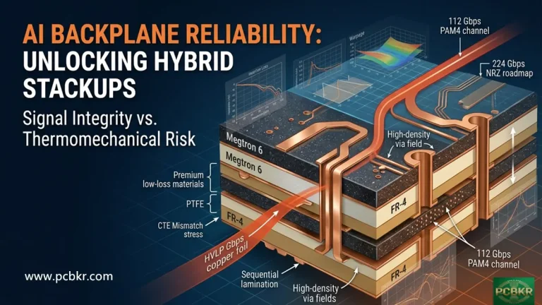
AI server high-speed interconnect: As AI accelerator cards push signal rates past 112 Gbps PAM4, the channel loss budget on backplane and mezzanine boards depends heavily on dielectric selection — a controlled impedance PCB prototype on Rogers material validates the channel model before tooling is cut.
Critical Design and Manufacturing Considerations for High-Frequency PCBs in 2026
The following section covers the engineering principles that separate a functional RF PCB from one that meets specification from the first article. These considerations apply whether you are designing for 2.4 GHz Wi-Fi or 77 GHz radar.
1. Controlled Impedance PCB Design: 50Ω, 75Ω, and Differential Pairs
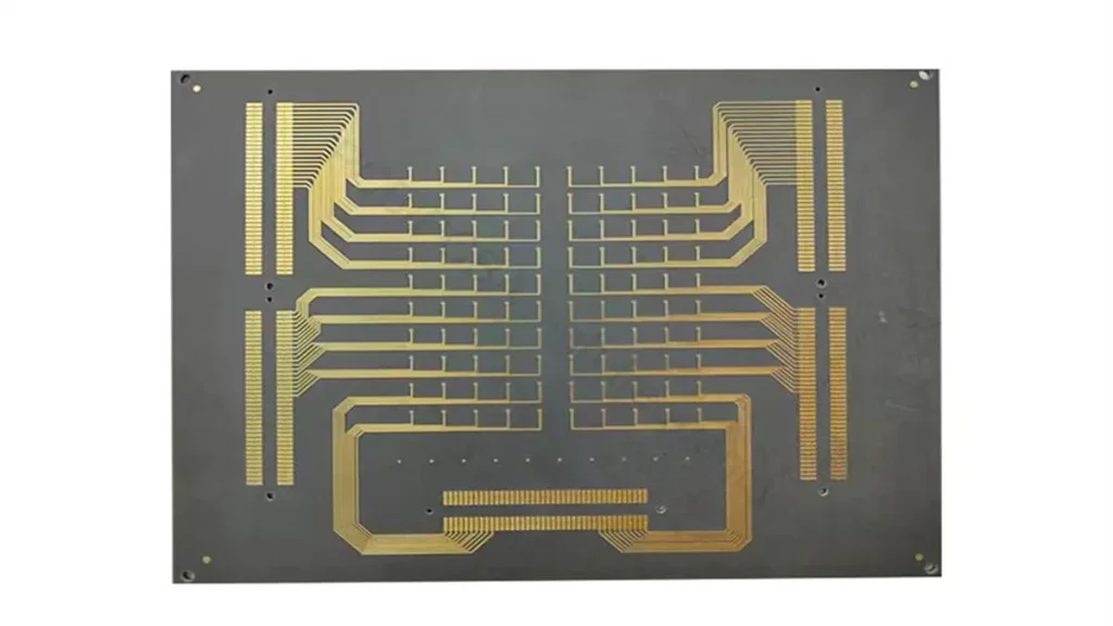
An unpopulated high-frequency test PCB manufactured by Hongda, featuring precision-etched 50Ω microstrip lines and high-uniformity ENIG surface finish for optimal signal integrity.
Impedance discontinuities reflect energy back toward the source and degrade noise figure in low-signal chains. Hongda supports controlled impedance PCB fabrication to ±5% or ±10% tolerance across all standard reference configurations:
- 50Ω single-ended microstrip (most RF/Microwave applications)
- 75Ω single-ended (cable TV, broadcast RF)
- 100Ω differential stripline (high-speed SerDes, USB 3.x, PCIe)
- Coplanar waveguide with ground (GCPW) for improved isolation
2. Surface Finish Selection: ENIG vs Immersion Silver
ENIG (Electroless Nickel Immersion Gold) provides excellent solderability, a flat surface ideal for fine-pitch QFN and BGA components, and good shelf life. The nickel layer does introduce a slight resistive loss at very high frequencies due to its magnetic permeability — a factor that becomes significant above approximately 30 GHz.
Immersion Silver (ImAg) eliminates the nickel layer entirely, reducing skin-effect losses at millimeter-wave frequencies. ImAg is increasingly specified for 5G FR2 antenna boards, automotive radar, and satellite links. Its primary tradeoff is shorter shelf life and sensitivity to sulfur compounds in storage environments.
3. Via Design for High-Frequency Boards
Through-hole vias in high-frequency designs create stubs that resonate and cause signal degradation. The 2026 standard practice for multilayer Rogers boards above 10 GHz includes backdrill (controlled-depth drilling) to remove the unused portion of via barrels, and laser via structures for fine-pitch blind/buried connections. Our process supports backdrilling to ±50 μm depth tolerance.
4. Latest PCB Manufacturing Technology in 2026
The year 2026 has brought meaningful advances to high-frequency PCB fabrication that directly benefit prototype customers:
- AI-assisted DFM analysis: Machine learning models pre-screen Gerber files for high-frequency specific issues such as impedance discontinuities, via stub depth predictions, and copper-to-edge clearances before a human engineer reviews the job
- Direct imaging (LDI) with 5 μm resolution: Eliminates film artwork tolerances that would otherwise widen conductor edges, improving impedance repeatability on narrow traces at millimeter-wave frequencies
- Automated impedance measurement: Inline TDR testing at 100% panel coverage replaces statistical coupon sampling, catching outlier impedance values before boards leave the line
- Plasma de-smear for Rogers PTFE laminates: Improves via wall cleanliness and copper adhesion in RO3003 and RT/duroid constructions, reducing the incidence of plating voids in small-diameter drill holes
Quality Control and Testing Capabilities
A Rogers PCB prototype that cannot be tested and verified against specification provides no useful data for the design team. Our quality system is built around measurements that matter for RF and high-frequency digital applications.
1. TDR Impedance Testing
Every production panel receives TDR (Time Domain Reflectometry) testing on representative coupons. Results are captured in an impedance report that we provide with your shipment. Values outside the specified tolerance window trigger a hold and root-cause investigation before boards are released.
2. AOI and X-Ray Inspection
Automated optical inspection (AOI) checks outer-layer conductor geometry, pad dimensions, and solder mask registration. For blind and buried via structures, X-ray inspection verifies drill registration and copper fill quality in via holes that cannot be inspected optically. These steps are standard on all Rogers PCB orders, not optional upgrades.
3. Material Certification
Hongda sources all Rogers laminates directly from authorized distributors and maintains material certificates traceable to Rogers Corporation lot numbers. Customers who require traceability for aerospace, defense, or automotive programs can request lot-level documentation at the time of order.
Application Case Studies
1. 5G mmWave Antenna Module Prototype — 48-Hour Delivery
A communications hardware startup needed six prototype panels of a 39 GHz phased-array antenna board on RT/duroid 5880. The design required GCPW transmission lines with a target impedance of 50Ω ±5% and Immersion Silver surface finish to preserve conductor conductivity at millimeter-wave frequencies. From Gerber submission to shipping took 47 hours. The customer’s network analyzer measurements confirmed insertion loss within 0.3 dB of their simulation model.
2. Automotive Radar PCB Prototype on RO3003
An automotive Tier 1 supplier validating a 77 GHz long-range radar transmit/receive module submitted a 6-layer hybrid stackup: two Rogers RO3003 layers for the RF front end and four FR-4 layers for power distribution and digital processing. Hongda’s standard hybrid multilayer PCB fabrication process delivered boards in 48 hours with TDR-verified 50Ω microstrip lines and full backdrill on the RF section vias.
3. AI Server High-Speed Interconnect Validation
A hyperscaler’s hardware team needed a quick-turn evaluation board for a 112 Gbps PAM4 re-timer device. The design used RO4350B for the high-speed differential pairs and required 100Ω controlled impedance to ±5%. Our AI-assisted DFM review flagged a via antipad spacing issue on the differential pairs that would have degraded return loss above 28 GHz. The customer updated the file within two hours and boards shipped the following day.
How to Order Your Rogers PCB Prototype from Hongda
The ordering process is designed to minimize friction for engineering teams who are focused on getting results, not managing supplier paperwork.
Step 1: Submit Your Gerber Files
Upload your Gerber files along with a stackup drawing, drill file, and impedance requirements. Our online portal accepts RS-274X Gerber format, ODB++, or IPC-2581. If you are not yet sure of your exact stackup, our application engineering team can recommend one based on your frequency band and impedance target.
Step 2: Select Material and Turnaround
- Choose your Rogers grade: RO4350B, RO4003C, RO3003, RT/duroid, RO4835, RO4360G2, or hybrid stackup
- Specify copper weight: 0.5 oz, 1 oz, or 2 oz
- Select surface finish: ENIG, Immersion Silver (ImAg), OSP, or HASL
- Choose turnaround: 48-hour standard or 24-hour expedited
Step 3: Engineering Review and Confirmation
Within two business hours of submission, our engineers complete the free DFM check and return a confirmed quote with impedance stackup drawing. You approve the quote and production begins immediately.
Step 4: Production, Test, and Ship
Your boards are fabricated, tested to the specifications above, and shipped the same day production completes. Impedance reports and material certificates are emailed with the tracking number.
Why Choose Shenzhen Hongda Circuit Technology Co., Ltd.
There is no shortage of PCB manufacturers in Shenzhen. What differentiates Hongda in the Rogers prototype segment specifically comes down to four operational capabilities:
- Rogers material on-shelf inventory across all major grades eliminates the 3–5 day laminate procurement delay that plagues most mid-size PCB shops
- Dedicated high-frequency fabrication line with process parameters tuned specifically for PTFE and hydrocarbon-ceramic laminates
- 24–48 hour fast-turn PCB prototyping as a standard offering, not a special exception that requires management approval
- No MOQ policy that supports single-board orders at production-equivalent quality, enabling iterative development without cost penalties
- In-house TDR impedance testing with 100% panel coverage and customer-facing impedance reports
- Free DFM check with same-day turnaround on Gerber review for RF and high-speed designs
Ready to Start Your Rogers PCB Prototype?
Upload your Gerber files today and receive a confirmed quote and free DFM report within two business hours. Shenzhen Hongda Circuit Technology Co., Ltd. is ready to support your next 5G, radar, AI server, or microwave design with the speed and quality your program demands.
Email: sales@pcbkr.com
Website: www.pcbkr.com
FAQ
What is the standard turnaround time for a Rogers high-frequency PCB prototype?
For standard engineering and development runs, a typical prototype order follows a 48-hour production schedule. However, for time-critical programs or tight verification sprint cycles, an expedited 24-hour delivery channel is available, which allocates reserved machine time and a dedicated process engineer to ensure next-business-day shipping.
Is there a Minimum Order Quantity (MOQ) for custom Rogers RF PCB orders?
No, there is a strict no minimum order quantity (No-MOQ) policy for high-frequency prototype development. Procurement teams can order single-board quantities for first-pass electrical evaluation or run multiple design variants simultaneously to compare S-parameters without facing any price penalties or re-qualification fees.
How can we reduce the manufacturing cost of a high-frequency Rogers PCB?
The most effective strategy to control material costs is deploying a Rogers-FR4 hybrid stackup. This structural approach isolates the critical RF transmission lines on the premium Rogers laminate while placing standard digital and power routing layers on economical FR-4, significantly lowering overall material expenses without sacrificing signal integrity.
Which surface finish should be selected for a 5G or millimeter-wave radar prototype: ENIG or Immersion Silver?
The choice depends heavily on your operating frequency. ENIG provides excellent solderability and a flat surface for fine-pitch BGAs, but its nickel layer introduces slight resistive losses above 30 GHz due to magnetic permeability. Immersion Silver (ImAg) eliminates the nickel layer entirely, minimizing skin-effect insertion losses, making it the preferred standard for 5G FR2 antennas and 77 GHz automotive radar modules.
What quality control documentation and reports are provided with a Rogers PCB prototype shipment?
Every high-frequency manufacturing panel undergoes 100% inline TDR (Time Domain Reflectometry) impedance testing to verify that 50Ω, 75Ω, or 100Ω differential lines fall within the target $\pm5\%$ or $\pm10\%$ tolerance window. Concurrently, shipments include a comprehensive customer-facing impedance report, AOI/X-ray verification logs for blind/buried vias, and material certifications traceable directly to Rogers Corporation lot numbers.
About Author
David Chen https://www.linkedin.com/in/pcbcoming
David Chen boasts an extensive professional background in PCBA manufacturing, PCBA testing, and PCBA optimization, with specialized expertise in high-precision PCBA fault analysis and rigorous PCBA reliability testing. The author has worked with high-layer-count server PCB fabrication, ultra-low-loss backplane stackups, and thermo-mechanical reliability optimization for AI infrastructure projects involving 112G and 224G PAM4 architectures. Skilled in complex circuit design and cutting-edge advanced PCB manufacturing processes, he delivers solutions that elevate product durability and performance across industrial applications. His technical articles focusing on PCBA manufacturing workflows and testing methodologies are widely cited by industry peers, research institutions, and technical platforms, solidifying his reputation as a recognized technical authority in the global circuit board manufacturing sector.