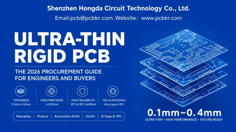
Custom Ultra‑Thin PCB Manufacturing: A Procurement Engineer’s Guide to Specifications, Advanced Fabrication Technology, and Supplier Qualification
The Procurement Risk Nobody Talks About Until It Fails
Custom ultra thin PCBs with fine-pitch features, microvias and controlled-impedance differential pairs are widely specified by electrical engineers to meet the miniaturization demands of compact electronic devices. Meanwhile, mechanical design teams usually adopt stringent internal housing clearance designs to pursue higher space utilization. The conflicting high-precision requirements of electrical performance and mechanical assembly create huge manufacturing and application challenges for ultra-thin circuit boards, severely affecting new product introduction (NPI) progress.
In actual hardware development projects, when hardware teams issue RFQs for custom PCBs with a finished thickness below 0.6 mm, unanticipated dimensional deviation and thermal-mechanical deformation of the boards frequently delay NPI timelines. A typical engineering scenario fully reflects this pain point: if the product enclosure only reserves 2.3 mm of internal assembly clearance, engineers will customize a 0.2 mm four-layer ultra-thin PCB equipped with 50 μm microvias and impedance-controlled differential pairs to adapt to the compact space. However, after prototype delivery, the actual finished board thickness often reaches 0.24 mm — a 20% overrun of the design target. Worse still, the board warpage rate can hit 0.9% after reflow soldering.
Such manufacturing deviations trigger a series of assembly and functional failures. The excessive board thickness and warpage directly lead to mechanical fitting failure between the PCB and enclosure, cause offset alignment of camera modules and other precision components, and ultimately push back the entire NPI schedule by several weeks, bringing extra time cost and risk to product development.
All these setbacks are essentially attributed to the unique physical limitations of ultra-thin PCB substrates. Conventional PCB manufacturing processes and standard workflows are no longer applicable to boards with a finished thickness of less than 0.6 mm. In the lamination stage, conventional high lamination pressure is prone to crushing fragile thin substrate cores, resulting in uneven board thickness. During the photolithography process, traditional contact-print phototools will stretch when applied to 0.15 mm ultra-thin substrates, causing fine-pitch circuit pattern deviation. In the drilling process, conventional mechanical drilling technology also faces great risks, which may easily crack the ultra-thin dielectric layers and damage circuit structures.
This professional guide is tailored for procurement engineers, supply-chain managers and hardware project leads. Centering on custom ultra-thin circuit board development and sourcing, it systematically sorts out core key points covering product specification definition, PCB stack-up design optimization, high-adaptability material selection and standardized RFQ best practices. In addition, this guide also supports complete supplier capability assessment, production equipment verification and factory qualification process formulation, providing comprehensive technical and process guidance for the stable mass production and reliable application of custom ultra-thin PCBs.
What Is a Custom Ultra‑Thin PCB? Thickness Standards and Material Specifications
The 0.6 mm Threshold: Ultra‑Thin vs. Thin PCB Classification
Industry‑accepted thickness groupings help prevent miscommunication during BOM creation and RFQ submission. Mislabeling board thickness categories commonly generates quoting discrepancies and prototype mismatches.
| Classification | Finished Thickness | Typical Applications | Fabrication Complexity |
|---|---|---|---|
| Standard PCB | 1.0mm – 2.0mm | Industrial controls, power supplies | Conventional |
| Thin PCB | 0.4mm – 0.6mm | Consumer electronics, compact modules | Moderate |
| Ultra‑Thin PCB | 0.1mm – 0.4mm | Wearables, medical implants, camera modules, smartcards, IoT sensors | High |
Procurement Note: Avoid loose terminology inside RFQ documents. Many buyers interchange “thin PCB” and “ultra‑thin PCB”. If your target finished thickness equals 0.2 mm, always state exact thickness plus tolerance in your technical package, rather than relying on generic descriptive labels.
A 0.1 mm‑0.4 mm custom ultra‑thin PCB cannot be treated as a mechanically scaled‑down conventional PCB. At 0.2 mm finished thickness, dielectric cores may be as slim as 0.05 mm FR4 or 0.025 mm polyimide. Copper foil is reduced to 12 μm‑18 μm. Safe lamination pressure windows shrink sharply compared with standard‑thickness boards. If fabricators reuse 1.6 mm PCB process recipes for ultra‑thin builds, defects such as delamination, resin starvation and excessive thickness variation will occur.
Material Platforms for Custom Ultra‑Thin Circuit Boards: FR4, PI, and BT Resin
Substrate material selection directly determines assembly survivability and long‑term field reliability for ultra‑thin hardware designs. Three mainstream material families apply for rigid and rigid‑flex ultra‑thin PCBs:
• Ultra‑Thin FR4: Glass‑reinforced epoxy cores available down to 0.05 mm. This is the cost‑effective baseline for rigid ultra‑thin PCBs exposed to moderate thermal cycling. Standard Tg ranges from 130 °C‑140 °C; high‑Tg grades reach 170 °C for industrial and automotive hardware.
• Polyimide (PI): Base material starting at 0.025 mm thickness with outstanding thermal stability and dynamic flex endurance. It is mandatory for flex and rigid‑flex ultra‑thin PCB implementations inside wearables and medical devices. PI withstands repeated bending far better than FR4 but carries 2‑3× higher material cost.
• BT Resin: Bismaleimide‑triazine laminate with Tg ≥200 °C and low moisture absorption. Specify BT resin for high‑reliability ultra‑thin circuit boards deployed within aerospace, defense and implant‑grade medical electronics, where thermal‑shock and humidity resistance are critical requirements.
Procurement Tip: When your assembly profile exceeds 245 °C reflow temperature or devices require hermetic sealing, explicitly call out high‑Tg FR4 or BT resin within your material specification. Standard low‑Tg FR4 thinner than 0.2 mm can develop micro‑cracks under thermal shock; such failures often only surface during environmental stress screening.
Core Fabrication Capabilities Shaping Ultra‑Thin PCB Design Rules

Picosecond UV Laser Microvia Drilling on Custom Ultra-Thin PCB
Producing reliable ultra‑thin PCBs relies on specialized manufacturing workflows, which set hard limits for your layout, stack‑up and feature sizing. Four core technical capabilities define feasible design boundaries:
- Laser Direct Imaging (LDI): Eliminates physical phototool‑related stretching and misalignment. LDI delivers ±5 μm layer‑to‑layer registration and supports 56 μm/56 μm line‑and‑space geometry on 0.1 mm‑0.2 mm thin cores. It is essential for fine‑pitch BGA fan‑out and dense camera‑module interconnect layouts.
- Modified Semi‑Additive Process (mSAP): Builds traces from thin copper seed layers rather than etching down thick copper foils. It achieves near‑vertical trace sidewalls and supports 8 μm/8 μm fine‑line structures, improving impedance consistency for high‑density ultra‑thin HDI designs.
- Vacuum‑Assisted Lamination: Zone‑controlled low‑pressure curing mitigates thermally induced stress mismatch between copper and dielectric materials. This process keeps board warpage below the 0.5 % threshold required for SMT assembly and prevents resin squeeze‑out or delamination on ultra‑thin multilayer stacks.
- Picosecond UV Laser Drilling: Forms clean 50 μm‑scale microvias within ultra‑thin dielectrics without core fracture or burring seen with mechanical drilling. Positional accuracy holds at ±5 μm for sequential‑lamination HDI constructions.
Full technical deep‑dives, equipment benchmarks and supplier‑verification checklists for these processes are covered in our dedicated supplier‑qualification resource: Ultra‑Thin PCB Supplier.
Custom Ultra‑Thin PCB Manufacturing Capabilities: A Procurement Engineer’s Checklist
Use this checklist to translate mechanical‑electrical requirements into concrete technical specifications for your RFQ.
Layer Count and Stack‑Up Design for 0.1mm to 0.6mm Builds
| Layer Count | Minimum Thickness | Typical Stack‑Up | Application |
|---|---|---|---|
| Single‑sided | 0.08mm | 0.05mm core + 12μm copper | Smartcard antennas, simple flex |
| Double‑sided | 0.13mm | 0.05mm core + 2×12μm copper + plating | Basic IoT sensors, LED strips |
| 4‑layer | 0.35mm | 2×0.05mm core + 2×40μm prepreg + copper | Camera modules, compact controllers |
| 6‑layer | 0.50mm | 3×0.05mm core + prepreg + copper | High‑density wearables |
Critical stack‑up constraint: All multi‑layer ultra‑thin PCBs require symmetric stack‑up architecture. Mirror copper weight, core thickness and prepreg quantities across the board central axis. Asymmetric copper distribution (for example, 1oz copper on layer 1 versus 0.5oz copper on layer 4) creates residual thermal stress that manifests as board warpage after reflow.
Copper Weight, Trace Geometry, and Microvia Specifications
• Copper Weight: 0.5oz (17 μm) and 1oz (35 μm) represent standard selections for ultra‑thin PCB builds. 2oz copper is technically achievable but increases lateral‑etch risk on fine traces. For 0.1 mm‑0.2 mm boards, stick to 0.5oz copper unless high‑current‑carrying performance forces heavier copper selection. • Trace/Space: 2.2mil/2.2mil (56 μm/56 μm) achievable with LDI subtractive processing; 8 μm/8 μm for mSAP build‑up layers. • Microvias: 50 μm‑100 μm laser‑drilled blind vias. Maintain 1:1 aspect ratio across 25 μm‑50 μm dielectrics. Stacked microvias up to four‑layer depth are supported for HDI ultra‑thin PCB layouts. • Minimum Hole: 0.1 mm mechanical PTH only feasible for boards ≥0.3 mm; exclusively laser‑drilled vias for thickness below 0.3 mm.
Surface Finishes and Panelization Options for Thin PCB Boards
• ENIG (Electroless Nickel Immersion Gold): Flat surface, strong oxidation resistance, well‑suited for fine‑pitch SMT and wire‑bonding workflows. Widely adopted for camera‑module and medical‑device ultra‑thin PCBs. • OSP (Organic Solderability Preservative): Cost‑effective planar finish with limited shelf‑life; recommended for consumer wearables with fast assembly turnaround cycles. • ENEPIG: Nickel‑palladium‑gold finish optimized for aluminum wire‑bonding and harsh operating environments, specified for aerospace and implant‑capable medical hardware. • Panelization: Maximum finished panel dimensions 500×650 mm or 1200×450 mm; minimum standalone piece size 3×3 mm. For ultra‑thin panels, specify tab‑routing with support rails instead of V‑scoring to avoid edge cracking during depanelization.
Application‑Specific Design Guidelines for Custom Ultra‑Thin PCBs
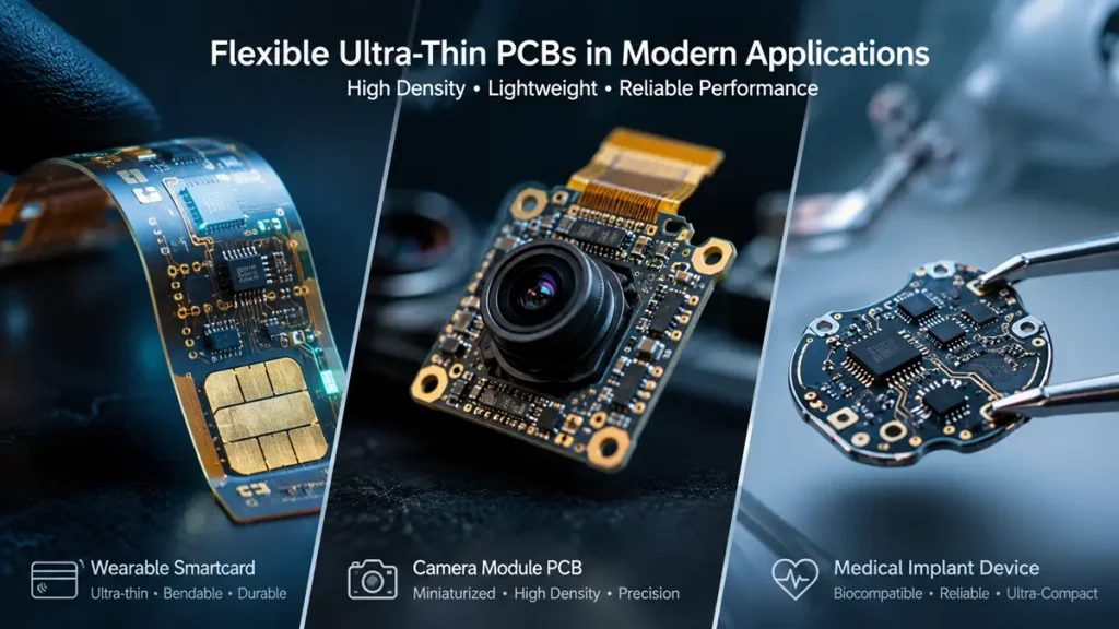
Custom Ultra-Thin PCB Applications in Wearables, Camera Modules, and Medical Devices
Wearable Electronics and Smartcard Modules: Flexure and Insertion Survival
Ultra‑thin PCBs inside wearables must withstand torsional stress from wrist‑band flexing or physical card insertion. Follow these design rules to improve mechanical endurance:
• Deploy PI coverlay instead of standard solder mask for dynamically flexing zones. Select 25 μm‑50 μm‑thick coverlay to distribute mechanical stress across bend radii. • Route copper traces perpendicular to the primary bending axis. Traces aligned parallel to bending directions concentrate stress and fracture after 5 000‑10 000 flex cycles. • Specify 0.5oz copper to reduce stress concentration along trace edges. Heavier copper foils crack more readily under cyclic deformation. • Maintain bend radius ≥ 10 × total board thickness. For a 0.2 mm ultra‑thin flexible PCB, the minimum safe bend radius equals 2 mm.
BOM drafting reminder: Explicitly define coverlay material and thickness within your drawing notes, rather than leaving flex‑region material choices open to fabricator interpretation.
Camera Module Substrates and Compact IoT Sensors: HDI in Minimal Z‑Height
Camera‑module hardware demands high‑density interconnects while enforcing strict vertical‑height constraints. Key design specifications:
• Adopt 2+ layer HDI stack‑up with 50 μm laser microvias and via‑in‑pad (VIPPO) structures to maximize routing density within limited Z‑space. • Select ENIG for gold‑wire‑bond compatibility; choose ENEPIG when enhanced bond‑reliability under environmental exposure is required. • Reserve routing tolerance ±0.05 mm for lens‑alignment fiducials. Any fiducial positional deviation shifts optical paths and degrades final image performance. • Enforce impedance‑control targets for MIPI or LVDS differential pairs. On 0.1‑0.2 mm‑thick dielectrics, impedance values are highly sensitive to trace‑width variance. Include impedance‑simulation outputs alongside your Gerber deliverables.
Medical Implant Devices and Aerospace Avionics: Reliability at Minimum Thickness
For implantable or body‑worn medical hardware, ultra‑thin PCB design prioritizes biocompatibility and multi‑year operational reliability:
• Select high‑Tg BT resin or ceramic‑filled laminates for enhanced moisture resistance and thermal stability. • Specify ENEPIG surface finish for wire‑bonded circuits inside hermetic packages. Standalone ENIG may suffer nickel corrosion under prolonged high‑humidity exposure. • Default thickness tolerance setting: ±10 %; tighten to ±5 % for critical implant applications. Tighter thickness tolerances require closed‑loop lamination‑press process control and typically add 15‑20 % to unit‑piece cost. • Enforce full material traceability and IPC Class 3 inspection requirements. Require traceability linking every core laminate lot, copper‑foil batch and prepreg roll to finished‑panel serial numbers.
The Procurement Decision Chain: From RFQ to Volume Production
Stage 1 – Specification Documentation: What to Include in Your Custom Ultra‑Thin PCB RFQ
Incomplete RFQ submissions trigger repeated engineering clarifications and delay formal quoting timelines. Consolidate these technical items before sending requests for quotation:
- Exact finished‑thickness value plus formal tolerance (example: 0.2 mm ±0.02 mm). Avoid vague phrasing such as “as thin as possible”.
- Total layer count plus proposed stack‑up drawing, or request stack‑up recommendations from your fabricator.
- Full material specification: FR4 Tg rating, PI or BT resin. Include material brand and grade if pre‑qualified.
- Defined copper weight for every signal/power layer. Note that 2oz outer‑layer copper complicates fine‑line etching on thin dielectric cores.
- Microvia requirements: finished diameter, pad dimension, fill type (conductive paste, copper plating, unfilled), and whether vias adopt stacked or staggered architecture.
- Required surface finish: ENIG, OSP, ENEPIG, immersion silver, or alternative finishes.
- Impedance‑control targets with reference‑plane definition and tolerance windows.
- Panelization rules: break‑tab or scoring preference, fiducial requirements, tooling‑hole pattern.
- Volume and delivery expectations: prototype quantity, pre‑production validation batch size, and annual‑volume forecast.
- Special compliance requirements: RoHS, REACH, halogen‑free, UL certification, ISO 13485 medical compliance or IATF 16949 automotive compliance.
At Hongda Circuit, a ready‑built Custom Ultra‑Thin PCB RFQ Checklist captures all critical technical parameters. Engineering teams submitting complete documentation normally receive formal quotes within 24 hours, avoiding rounds of back‑and‑forth clarification.
Stage 2 – Supplier Capability Audit
ISO‑9001 certification alone cannot validate ultra‑thin‑PCB manufacturing competence. Full audit matrices, equipment‑verification workflows and SPC‑data evaluation guidance are covered inside our supplier‑qualification article Ultra‑Thin PCB Supplier.
Practical procurement tip: Before awarding orders, request cross‑section photomicrograph samples and process‑capability evidence for ultra‑thin builds matching your stack‑up complexity.
Stage 3 – Prototype Validation and First Article Inspection
Always complete formal First Article Inspection (FAI) for ultra‑thin PCB prototypes. Minor thickness deviation on 0.2 mm boards creates catastrophic mechanical‑fit failure once high‑volume manufacturing commences.
From a procurement‑engineer perspective, require your fabricator to deliver the following FAI outputs together with prototype shipments:
- Cross‑section analysis sampled across multiple panel locations, verifying copper thickness, dielectric height, microvia fill quality and annular‑ring integrity.
- 9‑point thickness‑mapping results measured with digital micrometers (readout precision ±0.001 mm).
- Warpage test data measured via shadow‑moiré testing under simulated reflow thermal profiles.
- Thermal‑shock test reports (per IPC‑TM‑650 Method 2.6.7, −40 °C to +125 °C for 1 000 cycles) for medical‑grade and automotive‑grade hardware.
Best Practice: Require FAI datasets to ship alongside physical prototypes. Resolve thickness‑variation or warpage risks before locking production tooling.
Stage 4 – Volume Procurement and Supply‑Chain Integration
After prototype validation passes, implement structured supply‑chain management for scaled‑up production:
- Use blanket purchase orders with scheduled release schedules to lock‑in pricing for specialty thin‑core materials (0.025 mm PI, 0.05 mm FR4), subject to raw‑material market volatility.
- Deploy Kanban or VMI inventory programs for customers consuming 5 000+ panels monthly. Qualified fabricators maintain safety stock of pre‑validated thin‑core laminates to mitigate component‑allocation risks.
- Secure emergency‑order response agreements for medical‑device and aerospace projects. Even short‑term stock‑outs of 0.15 mm ultra‑thin PCBs can halt implant‑device assembly‑line operations.
Quality Control and Reliability Assurance for Ultra‑Thin Circuit Boards
Quality for ultra‑thin PCBs is built during fabrication rather than detected only at final‑test stages. When defining your acceptance criteria, specify these key in‑process inspection deliverables from your manufacturer:
• AOI inspection after inner‑layer etching, to flag opens, shorts and insufficient annular‑ring defects on fine‑geometry traces. • Automated optical alignment validation for LDI imaging, halting production if inter‑layer misalignment exceeds ±10 μm. • Multi‑point post‑lamination thickness gauging for every production panel. Measurement data feeds back into lamination‑recipe tuning to prevent process drift lot‑to‑lot. • X‑ray inspection for stacked‑microvia structures, verifying via fill completeness and absence of internal voids.
Detailed Cpk / SPC statistical‑process‑control benchmarks for ultra‑thin‑PCB fabrication are available in our supplier‑qualification guide.
Frequently Asked Questions by Procurement Engineers Sourcing Custom Ultra‑Thin PCBs
What is the minimum thickness achievable for a custom ultra‑thin PCB, and does layer count limit how thin the board can be?
Single‑layer ultra‑thin PCBs can reach 0.08 mm finished thickness built upon 0.05 mm FR4 core with thin‑clad copper. Double‑sided constructions bottom‑out near 0.13 mm. Multilayer stack‑ups impose higher physical limits: a 4‑layer ultra‑thin PCB can achieve 0.35 mm total thickness, which relies on 0.05 mm cores, 0.04 mm prepregs and low‑pressure vacuum‑lamination processes to avoid resin squeeze‑out. Six‑layer designs at 0.50 mm are feasible but demand strict symmetric‑stack‑up implementation for warpage mitigation. Always request stack‑up simulation outputs before finalizing multi‑layer designs below 0.4 mm.
How do I control thickness tolerance when procuring custom thin PCBs in volume?
Specify ±10 % thickness tolerance formally within your purchase‑order documentation, and mandate multi‑point post‑lamination thickness inspection reports for every production lot. For high‑mission‑critical hardware such as medical implants or aerospace sensors, you may negotiate tightened ±5 % tolerance via closed‑loop lamination‑press controls. This upgrade adds 15‑20 % to unit cost and should be negotiated during RFQ evaluation, not after prototype delivery.
Can an ultra‑thin PCB manufacturer support both rigid and flexible ultra‑thin circuit boards in the same production facility?
Rigid ultra‑thin PCBs (0.1 mm‑0.4 mm FR4 / BT resin) and flexible ultra‑thin PCBs (0.025 mm‑0.2 mm PI) share imaging and laser‑drilling equipment, yet require separate handling for lamination and cover‑lay lamination. Confirm whether your fabricator owns dedicated flex‑processing infrastructure; otherwise flex‑related work may get outsourced, increasing lead‑time and quality risks.
What files and documentation should my RFQ include to get an accurate quote for custom ultra‑thin PCB prototyping?
Provide: (1) Gerber RS‑274X files plus drill files; (2) target finished thickness or preliminary stack‑up drawing; (3) layer count and material preferences (FR4 Tg / PI / BT); (4) copper‑weight definition for each layer; (5) surface‑finish specification; (6) microvia / blind‑via requirements including diameter and fill requirements; (7) impedance‑control targets if applicable; (8) quantity and delivery timeline; (9) panelization and depanelization requirements. For PCBA services, attach BOM and assembly drawings. More complete documentation enables earlier DFM risk identification before tooling begins.
Note: Guidance on validating real‑world 0.1 mm‑0.2 mm manufacturing capability from potential vendors is covered inside our supplier‑qualification article.
About Author
David Chen https://www.linkedin.com/in/pcbcoming
David Chen boasts an extensive professional background in PCBA manufacturing, PCBA testing, and PCBA optimization, with specialized expertise in high-precision PCBA fault analysis and rigorous PCBA reliability testing. The author has worked with high-layer-count server PCB fabrication, ultra-low-loss backplane stackups, and thermo-mechanical reliability optimization for AI infrastructure projects involving 112G and 224G PAM4 architectures. Skilled in complex circuit design and cutting-edge advanced PCB manufacturing processes, he delivers solutions that elevate product durability and performance across industrial applications. His technical articles focusing on PCBA manufacturing workflows and testing methodologies are widely cited by industry peers, research institutions, and technical platforms, solidifying his reputation as a recognized technical authority in the global circuit board manufacturing sector.