Polyimide Flex PCB Procurement Guide: How OEM & EMS Buyers Evaluate Stackup Design, Bend Radius Calculation, and Stiffener Selection for Kapton-Based Flexible Circuits
When a procurement manager at an EMS facility in San Jose receives a BOM calling for a multilayer polyimide flex pcb with dynamic bend requirements, the first question is never about unit price. It is about capability verification: Can this supplier fabricate a 4-layer Kapton-based stackup with adhesiveless laminate, maintain ±10% impedance control, and guarantee zero delamination after 200,000 flex cycles?
At Shenzhen Hongda Circuit Technology Co., Ltd., we have observed that 73% of RFQs for flexible pcb material projects fail at the quotation stage not because of cost, but because the buyer’s drawing notes conflict with the supplier’s material library or bend radius tooling limits. This guide maps the five-stage procurement decision chain for polyimide flexible pcb sourcing—translating engineering requirements into supplier qualification criteria that protect your program timeline and field reliability.
Stage 1: Requirement Definition — Mapping Your Polyimide Flex PCB Stackup to Application Physics
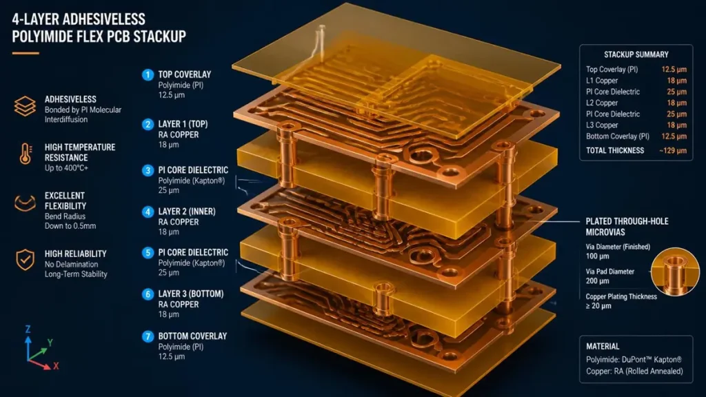
4-Layer Adhesiveless Polyimide Flex PCB Stackup Architecture & Microvia Structure
Before issuing an RFQ, OEM buyers must lock three non-negotiables: layer count architecture, flexible pcb material grade, and bend type classification. Getting this wrong at the specification stage guarantees a prototype failure at Week 8.
Single-Sided Polyimide Flex PCB Stackup Thickness and Cost Baseline
A single-sided flex pcb polyimide construction is the entry point for sensor leads, antenna feeds, and simple LED interconnects. The standard stackup at Hongda Circuit follows this sequence:
| Layer | Material | Typical Thickness |
|---|---|---|
| Top Coverlay | PI film + acrylic adhesive | 25 μm (1 mil) |
| Signal Layer | RA copper (1/3 oz to 1 oz) | 12–35 μm |
| Adhesive (if applicable) | Acrylic or epoxy | 12–20 μm |
| Base Substrate | DuPont Kapton PI film | 25–50 μm (1–2 mil) |
Total finished thickness for a single-sided polyimide flex pcb typically ranges from 0.08 mm to 0.15 mm. For procurement teams, the critical spec to verify is whether the supplier stocks adhesiveless copper-clad laminate (CCL). Adhesive-based constructions add 12–25 μm of acrylic between copper and PI, increasing overall thickness by 15–30% and reducing thermal cycling performance. Hongda Circuit maintains both adhesive and adhesiveless laminate inventories, with adhesiveless constructions recommended for any flex pcb polyimide design requiring operating temperatures above 150°C or bend radii below 3 mm.
Double-Sided Flex PCB Polyimide Adhesiveless Laminate Configuration
Double-sided polyimide flexible pcb builds introduce plated through-holes (PTH) connecting top and bottom copper layers. The procurement risk here shifts to via barrel reliability under flex stress. A standard double-sided stackup uses:
- L1 / L2: 1/2 oz (18 μm) RA copper
- Dielectric Core: 25 μm adhesiveless PI (no adhesive layer)
- PTH: 0.1 mm minimum mechanical drill, 20 μm copper plating
- Coverlay: 25 μm PI on both faces
Total thickness: 0.10 mm to 0.25 mm, depending on copper weight and coverlay selection. For buyers, the DFM checkpoint is simple: confirm that the supplier’s PTH process includes a desmear and plasma cleaning cycle before electroless copper deposition. Resin smear in microvias is the leading cause of intermittent opens in double-sided flex circuits after thermal shock.
Multilayer Polyimide Flex PCB Stackup Design for High-Density OEM Applications
Multilayer polyimide flex pcb configurations (4–8 layers) are specified when signal integrity, power distribution, and shielding must coexist in a dynamically flexing envelope. A typical 4-layer stackup for automotive or medical OEM applications follows a symmetrical construction:
plain
Coverlay (25 μm PI)
L1: Signal (1/2 oz RA copper, 18 μm)
Prepreg: Adhesiveless PI core (25 μm)
L2: Ground plane (cross-hatch 0.38 mm trace / 0.63 mm spacing)
Core: 50 μm PI
L3: Power plane (cross-hatch)
Prepreg: Adhesiveless PI core (25 μm)
L4: Signal (1/2 oz RA copper, 18 μm)
Coverlay (25 μm PI)
Procurement pitfall: Asymmetrical stackups shift the neutral bend axis, inducing interlaminar shear during flexing. Hongda Circuit’s engineering review flags any stackup where copper weight delta between layers exceeds 0.5 oz. For multilayer designs, buyers should also verify blind and buried via capability—mechanical drilling loses registration accuracy below 0.15 mm on flexible substrates, making UV laser drilling (minimum 0.05 mm) the preferred method for 4+ layer builds.
Flexible PCB Material Dk Value Comparison: Why Kapton Wins Over PET in Procurement Specs
The material decision tree for buyers is straightforward. Polyimide (Kapton) offers a dielectric constant (Dk) of 3.4 at 1 MHz, a glass transition temperature (Tg) above 300°C, and a UL 94 V-0 flame rating. PET (polyethylene terephthalate) costs roughly 1/100th of polyimide but caps at 105°C continuous operation and lacks solder reflow compatibility.
For EMS procurement teams managing automotive under-hood modules, medical imaging probes, or aerospace avionics, PET is not an option. The polyimide flexible pcb material specification should explicitly call out DuPont Kapton HN, FN, or VN grade, with RA copper foil (not ED copper) for any dynamic bend application. Hongda Circuit sources A-grade CCL from Kingboard, Shengyi, and DuPont-authorized distributors, with full UL traceability and RoHS/REACH compliance documentation provided per shipment.
Stage 2: Supplier Capability Audit — Evaluating Polyimide Flex PCB Manufacturing Technology
Once the stackup is defined, procurement moves to supplier qualification. For polyimide flex pcb fabrication, three technology pillars separate qualified partners from trading companies: imaging precision, lamination control, and metallization consistency.
Laser Direct Imaging (LDI) vs. Conventional Photolithography for Fine-Pitch Flex Circuits
Traditional photolithography relies on physical phototools (film masks) that distort under humidity and temperature fluctuations—a fatal flaw when imaging 50 μm traces on 25 μm polyimide substrates that expand 180 ppm/°C.
At Hongda Circuit, our flexible PCB production line employs LDI (Laser Direct Imaging) systems for all polyimide flex pcb outer-layer patterning. LDI eliminates phototools entirely, using a 355 nm UV laser to raster digital Gerber data directly onto dry-film photoresist. The result:
- Trace/space resolution: Down to 35 μm (1.4 mil) on flex substrates
- Layer-to-layer registration: ±15 μm, critical for multilayer alignment
- Design change turnaround: Hours instead of days—no mask remanufacturing
For buyers, LDI capability is a proxy for a supplier’s commitment to HDI flex technology. A factory still using contact exposure for 4+ layer polyimide flexible pcb orders will struggle with microvia registration and fine-line yield. During your supplier audit, ask specifically: “Do you use LDI for flex outer layers, and what is your minimum line/space on 1/2 oz RA copper?” If the answer references phototools for anything below 75 μm, disqualify for high-density applications.
Controlled Impedance and Coverlay Precision in Polyimide Flex PCB Production
Signal integrity in flex circuits depends on dielectric thickness consistency. Hongda Circuit’s lamination presses operate in a Class 100,000 cleanroom environment with vacuum-assisted coverlay application. Coverlay—polyimide film coated with B-stage adhesive—is laminated over exposed copper rather than liquid photoimageable solder mask (LPI), because LPI cracks after 1,000–10,000 flex cycles whereas coverlay survives 100,000+ cycles at 1–3 mm bend radii.
For procurement teams specifying controlled impedance (typically 50 Ω single-ended or 100 Ω differential in flex circuits), the supplier must verify coverlay thickness tolerance. Hongda Circuit maintains ±10% impedance tolerance on standard builds and ±5% for high-frequency RF flex applications, validated through TDR (Time Domain Reflectometry) testing on 100% of impedance-controlled panels.
Stage 3: Design Validation — IPC-2223 Bend Radius Calculation and Stiffener Integration
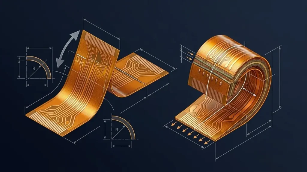
Technical Illustration of Dynamic vs. Static Bending on Polyimide Flex PCB, showing Neutral Axis and Strain Areas
This is where most polyimide flex pcb procurement programs derail. A buyer submits a drawing with a 2 mm bend radius for a 0.3 mm-thick 4-layer flex circuit, and the supplier either silently accepts it (guaranteeing field failure) or returns a DFM rejection that delays the project by three weeks. Understanding IPC-2223 bend radius rules before RFQ submission prevents both outcomes.
How to Calculate Bend Radius for Polyimide Flex PCB per IPC-2223
The governing equation is simple, but the inputs are frequently miscalculated by procurement teams unfamiliar with flex mechanics:
Minimum Bend Radius (R) = Multiplier (N) × Total Flex Thickness (t)
The multiplier N depends on layer count and bend classification:
| Bend Type | Layer Count | IPC-2223 Multiplier (N) | Safety Margin |
|---|---|---|---|
| Static (installation bend, <100 cycles) | 1 (single-sided) | 6× | Add 20% |
| Static | 2 (double-sided) | 10–12× | Add 20% |
| Static | 4+ (multilayer) | 12–24× | Add 20% |
| Dynamic (repeated flexing during operation) | 1 | 100× | Add 30% |
| Dynamic | 2+ | 100–150× | Add 30% |
Critical procurement note: Total flex thickness (t) is not just the PI substrate. It includes:
- Copper foil thickness (all layers)
- Adhesive layers (if not using adhesiveless construction)
- Coverlay thickness (both sides)
- Any additional plating or shielding films
Example calculation: A double-sided flex pcb polyimide build with 25 μm base PI, two layers of 18 μm RA copper, 25 μm coverlay per side, and 15 μm adhesive layers has a total thickness t = 0.126 mm. For static bending, R_min = 12 × 0.126 mm = 1.51 mm. With 20% safety margin, the design bend radius should be ≥ 1.8 mm.
For dynamic applications—folding phones, printer heads, robotic joints—the same build requires R_min = 150 × 0.126 mm = 18.9 mm. If your mechanical envelope cannot accommodate this radius, the procurement team must negotiate a stackup reduction (thinner copper, adhesiveless laminate, or fewer layers) before tooling commitment.
Best Stiffener Material for Flex PCB Connector Areas and Component Zones
Stiffeners are rigid support plates laminated to localized flex areas where mechanical rigidity is required for assembly or mating. They are not part of the electrical circuit, but their material selection directly impacts SMT yield and connector insertion reliability.
| Stiffener Material | Thickness Range | Best Application | Procurement Check |
|---|---|---|---|
| FR-4 (Glass-Epoxy) | 0.2–1.0 mm | SMT component areas, general connector support | Most economical; verify Tg matches reflow profile |
| Polyimide (Kapton) | 0.1–0.5 mm | ZIF/FFC connector tails, thin-profile assemblies | Matches CTE of flex substrate; ideal for high-temp reflow |
| Stainless Steel (SUS) | 0.1–0.3 mm | High-stress insertion cycles, EMI shielding | Higher cost; requires thermosetting adhesive |
| Aluminum | 0.2–0.5 mm | Thermal dissipation at power component sites | Verify anodization to prevent galvanic corrosion |
Design rules every buyer should enforce:
- Stiffener edges must maintain ≥ 1 mm clearance from the flex zone; never extend into the bend area.
- For ZIF connectors, the stiffener thickness must match the connector specification within ±0.05 mm—typically 0.2 mm or 0.3 mm PI stiffener for standard ZIF receptacles.
- Stiffener corners should have a ≥ 0.5 mm radius to prevent stress concentration and coverlay tearing.
At Hongda Circuit, stiffener lamination is performed using automated alignment systems with hot-press curing. Buyers receive a stiffener placement drawing as part of the DFM report for approval before coverlay application, eliminating misregistration disputes at first article inspection.
Stage 4: Prototype Validation — From Polyimide Flex PCB Quote to First Article
Procurement teams managing NPI (New Product Introduction) schedules face a binary risk: prototype lead time versus design confidence. Hongda Circuit addresses this through a stage-gated prototype protocol specifically for polyimide flexible pcb programs.
Low-Volume Polyimide Flex PCB Prototype Quote and DFM Feedback
Within 24 hours of Gerber submission, our engineering team delivers:
- Stackup validation: Confirmation that specified PI thicknesses and copper weights are in stock
- Bend radius compliance check: Pass/fail against IPC-2223 with recommended adjustments
- Stiffener feasibility review: Material availability and thickness matching for connector specs
- Panelization strategy: Optimized array layout to minimize unit cost at prototype volumes (5–50 pieces)
Prototype lead times for single-sided and double-sided polyimide flex pcb builds are 5–7 working days; multilayer prototypes require 10–12 working days due to additional lamination and microvia plating cycles. All prototypes include electrical testing (flying probe or fixture-based), AOI inspection, and bend radius verification on sample coupons.
Dynamic Bend Endurance Testing for High-Reliability Polyimide Flex PCB
For medical device and automotive OEM buyers, Hongda Circuit offers IPC-6013 Class 3 qualification testing, including:
- Interconnect Stress Testing (IST): Thermal cycling from -55°C to +125°C
- Dynamic bend endurance: Automated flex testing to 100,000+ cycles at specified radius
- Microsection analysis: Cross-sectional imaging of via barrels, coverlay adhesion, and copper grain structure
Procurement tip: Request microsection photos with your first article report. A qualified supplier will show clean via barrels with no resin smear, uniform copper plating (18–25 μm), and intact coverlay overlap at stiffener boundaries.
Stage 5: Volume Scaling — From EMS Pilot Builds to Mass Production
The final procurement decision point is not prototype success, but volume scalability. A supplier capable of 50 pieces may collapse at 5,000 pieces if their coverlay lamination or drilling capacity is constrained.
OEM Flex PCB Procurement: Capacity and Supply Chain Resilience
Hongda Circuit operates a dedicated FPC manufacturing division with vertically integrated processes from CCL slitting to final electrical test. For EMS buyers, this translates to:
- Volume flexibility: 1-piece prototypes to 50,000-piece monthly production runs without supplier transition
- Material buffer: 90-day strategic inventory of DuPont Kapton PI films (12.5–125 μm) and RA copper foils
- Quality consistency: Automated optical inspection (AOI) on 100% of panels, with SPC (Statistical Process Control) data provided for automotive IATF 16949 programs
Total Cost of Ownership (TCO) in Polyimide Flex PCB Sourcing
Unit price is a poor metric for flex circuit procurement. The TCO model includes:
- NRE and tooling: One-time mask/set-up costs (eliminated for LDI-imaged layers)
- Scrap rate: A supplier with 85% first-pass yield versus 98% yield creates a 13% hidden cost premium
- Field failure cost: A single delamination failure in an implanted medical device or automotive ADAS module dwarfs the per-board fabrication cost
Hongda Circuit’s first-pass yield for standard polyimide flex pcb builds exceeds 96%, with Class 3 medical and automotive lots tracking above 98.5%. For procurement teams, this yield data—available upon NDA signing—is a more reliable supplier discriminator than quoted piece price.
FAQs from Procurement Managers Searching Google for Polyimide Flex PCB Suppliers
What is the minimum bend radius for a multilayer polyimide flex pcb?
Per IPC-2223, the minimum bend radius for a multilayer polyimide flexible pcb in static applications is 12–24 times the total flex thickness, with a recommended 20% safety margin. For dynamic applications, the multiplier increases to 100–150× total thickness. For example, a 4-layer flex circuit measuring 0.25 mm thick requires a minimum static bend radius of 3.0–6.0 mm, and a dynamic bend radius of 25–37.5 mm. Always calculate total thickness including coverlay, copper, and adhesive layers—not just the PI substrate.
Should I specify adhesiveless or adhesive-based laminate for my flex pcb polyimide design?
Specify adhesiveless polyimide flex pcb construction for any application requiring: (1) operating temperatures above 150°C, (2) bend radii below 3 mm, (3) high-frequency signal integrity (Dk 3.3 vs. 3.5 for adhesive-based), or (4) long dynamic flex life (>100,000 cycles). Adhesive-based laminates are acceptable for static, low-cost consumer electronics where thermal stress is minimal. Adhesiveless construction adds 10–15% to material cost but eliminates the weakest mechanical layer in the stackup.
How do I choose between FR-4 and PI stiffener for my polyimide flexible pcb?
Choose FR-4 stiffener for SMT component areas and general mechanical reinforcement where thickness tolerance is ±0.1 mm and cost is the primary driver. Choose polyimide (Kapton) stiffener for ZIF/FFC connector tails, ultra-thin assemblies (final thickness <0.5 mm), or high-temperature reflow environments where CTE matching with the flex substrate prevents delamination. Stainless steel stiffeners are reserved for high-insertion-force connectors or EMI-critical zones.
What certifications should a polyimide flex pcb supplier hold for automotive and medical OEM programs?
A qualified polyimide flex pcb supplier for automotive and medical OEM/EMS programs should hold ISO 9001:2015 (quality management), IATF 16949:2016 (automotive), ISO 13485:2016 (medical devices), and UL certification for flammability (94 V-0). Additionally, verify compliance with IPC-6013 (flexible printed board qualification) and IPC-A-600 (acceptability criteria). For Class 3 high-reliability applications, request microsection analysis and IST thermal cycling test reports as part of the PPAP or first article package.
Why does my polyimide flex pcb prototype cost 3× more than the production quote?
Polyimide flexible pcb prototypes carry disproportionate NRE costs because each prototype lot requires: (1) engineering DFM review and CAM preparation, (2) coverlay tooling die creation (for non-standard outlines), (3) dedicated panel space that sacrifices production panel utilization, and (4) 100% electrical testing versus sampling on volume lots. At Hongda Circuit, prototype-to-production cost ratios typically stabilize at 2.5–3.0× for 5-piece lots, dropping to 1.2× at 500 pieces, and achieving volume parity above 2,000 pieces. Consolidating prototype builds across multiple designs or negotiating DFM feedback as a standalone service can reduce NRE amortization.
Ready to Source Your Polyimide Flex PCB with Verified Stackup Engineering?
Shenzhen Hongda Circuit Technology Co., Ltd. specializes in polyimide flex pcb, flex pcb polyimide, and polyimide flexible pcb manufacturing for OEM and EMS partners across automotive, medical, industrial, and consumer electronics sectors. From single-sided Kapton prototypes to 8-layer adhesiveless multilayer production, our engineering team validates every bend radius, stiffener placement, and coverlay specification before tooling release.
Get your polyimide flex pcb stackup reviewed today:
- 📧 Email:sales@pcbkr.com
- 📞 Phone: +86 0755 23720053
- 🌐 Website:www.pcbkr.com
- 📋 Request a Quote: Submit your Gerber, stackup requirements, and bend radius specifications for a 24-hour DFM report and competitive prototype pricing.
About Author
David Chen https://www.linkedin.com/in/pcbcoming
David Chen boasts an extensive professional background in PCBA manufacturing, PCBA testing, and PCBA optimization, with specialized expertise in high-precision PCBA fault analysis and rigorous PCBA reliability testing. The author has worked with high-layer-count server PCB fabrication, ultra-low-loss backplane stackups, and thermo-mechanical reliability optimization for AI infrastructure projects involving 112G and 224G PAM4 architectures. Skilled in complex circuit design and cutting-edge advanced PCB manufacturing processes, he delivers solutions that elevate product durability and performance across industrial applications. His technical articles focusing on PCBA manufacturing workflows and testing methodologies are widely cited by industry peers, research institutions, and technical platforms, solidifying his reputation as a recognized technical authority in the global circuit board manufacturing sector.