Voltage & Current Sampling Daughter Board: Design and Manufacturing Guide
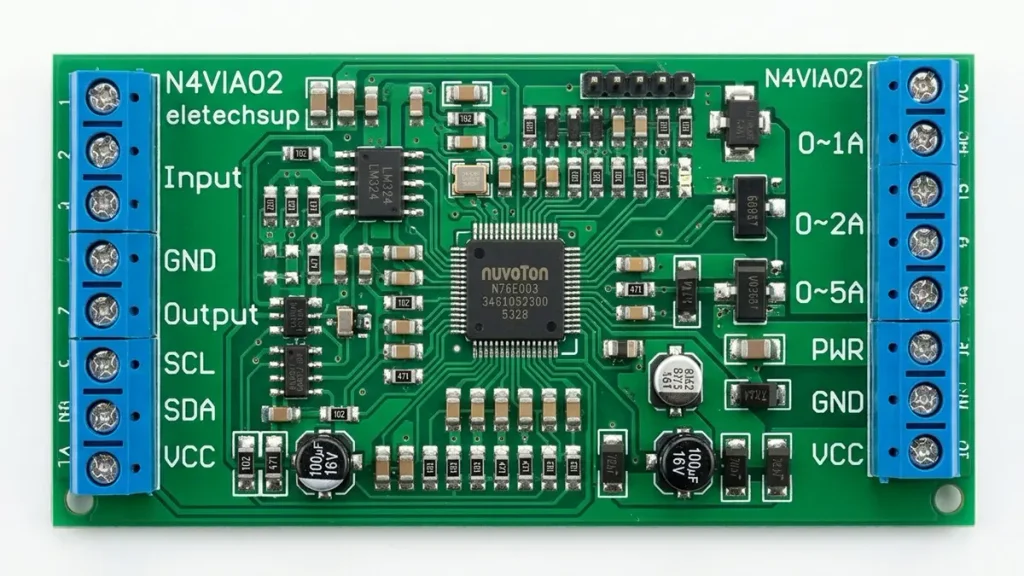
PCB Material: FR-4 / High-Tg FR-4
Layers: 2–8 Layers (design-dependent)
Board Thickness: Customized
Copper Thickness: Customized
Minimum Trace Width / Spacing: Customized
Minimum Hole Size: Customized
A Voltage & Current Sampling Daughter Board provides a dedicated circuit platform for acquiring voltage and current signals in power electronics, industrial control, battery management, motor drives, and energy monitoring systems. Its performance depends on more than the sensing components: signal conditioning, ADC architecture, PCB layout, isolation, component stability, assembly quality, and production testing all influence measurement reliability.
For OEMs and hardware developers, selecting the right manufacturing partner means evaluating both the electrical design requirements and the supplier’s ability to manufacture, assemble, inspect, and validate the board consistently from prototype to mass production.
1. Voltage & Current Sampling Daughter Board Overview
A Voltage & Current Sampling Daughter Board is a dedicated electronic module that measures electrical voltage and current signals and transfers the resulting analog or digital data to a main control board.
It is commonly used as a separate measurement section within a larger electronic system. This modular architecture allows engineers to isolate the sensing circuitry from the main processor, power-control circuitry, or communication functions. It can also simplify hardware upgrades, maintenance, and product customization.
A typical board may contain:
- Voltage-divider networks or dedicated voltage-sensing circuits
- Current-sensing resistors or magnetic current sensors
- Current-sense amplifiers and operational amplifiers
- Analog filters and signal-conditioning circuits
- Analog-to-digital converters (ADCs)
- Reference-voltage and power-management circuits
- Isolation components where required by the system architecture
- Connectors and communication interfaces for the main control board
The exact architecture depends on the operating voltage, current range, measurement resolution, sampling rate, isolation requirements, and host-controller interface.
1.1 Functional Architecture
The measurement process generally consists of four stages.
Signal acquisition: Voltage and current signals are obtained through voltage dividers, shunt resistors, Hall-effect sensors, or other suitable sensing elements.
Signal conditioning: The acquired signals are scaled, filtered, amplified, and protected to match the input requirements of the ADC or measurement IC.
Analog-to-digital conversion: The ADC converts conditioned analog signals into digital values. Its resolution, sampling rate, input range, reference stability, and noise performance affect the quality of the measurement.
Data communication: The sampled data is transferred to the main control board through interfaces such as SPI, I²C, UART, or another application-specific connection.
Separating these functions onto a daughter board can make the measurement circuitry easier to optimize and validate independently.
1.2 Daughter Board Integration in OEM Products
A sampling daughter board is usually designed around the electrical and mechanical requirements of its host product.
The design review should therefore cover more than the sensing circuit itself. Engineers should verify connector pin assignments, supply-voltage compatibility, signal levels, grounding strategy, mounting positions, board dimensions, thermal conditions, and communication timing.
For OEM projects, the daughter-board interface should be documented early in the development process. Changes to connector definitions, grounding, or signal routing late in development can create additional PCB revisions and system-level validation work.
2. Voltage and Current Sensing Technologies
The selection of a sensing technology determines the input range, measurement behavior, power dissipation, isolation architecture, and overall cost of the sampling board.
Different applications require different approaches. A low-current battery monitoring circuit, a motor drive, and an industrial power converter should not automatically use the same sensing architecture.
2.1 Shunt Resistor Current Sensing
Shunt-based sensing measures current by detecting the voltage drop across a low-resistance resistor.
The relationship is defined by Ohm’s law:
Vshunt = I × Rshunt
Where:
- Vshunt = Voltage drop across the shunt resistor
- I = Measured current
- Rshunt = Shunt resistance
For example, a 5 mΩ shunt carrying 10 A produces a 50 mV voltage drop. A current-sense amplifier or suitable ADC measures this voltage and converts it into a current reading.
Shunt sensing is widely used because it offers a direct measurement method, a relatively simple circuit architecture, and good suitability for precision current monitoring.
Important design considerations include:
- Shunt resistance and tolerance
- Temperature coefficient of resistance
- Power dissipation and thermal rating
- Common-mode voltage range
- Amplifier input offset and gain error
- Kelvin connection and PCB routing
- Required measurement bandwidth
The shunt resistor should be selected according to the maximum continuous current, peak current, allowable voltage drop, thermal conditions, and required measurement accuracy.
2.2 Hall-Effect Current Sensing
Hall-effect sensors measure the magnetic field generated by current flowing through a conductor. They can provide electrical isolation between the measured current path and the signal-processing circuit, depending on the sensor architecture.
This approach is useful when the system requires galvanic isolation, higher current measurement, or reduced insertion loss compared with a shunt-based approach.
However, engineers should evaluate sensor offset, temperature drift, linearity, bandwidth, magnetic interference, and the required calibration process.
Hall-effect sensing is not automatically more accurate than shunt sensing. The appropriate choice depends on the operating range, isolation requirements, thermal environment, cost target, and system-level error budget.
2.3 Voltage Divider and Dedicated Voltage-Sensing Circuits
Voltage sampling commonly uses a resistor divider to scale an input voltage into the measurable range of an amplifier or ADC.
The output voltage of a basic divider is:
Vout = Vin × R2 / (R1 + R2)
Where:
- Vout = Output voltage
- Vin = Input voltage
- R1 and R2 = Voltage divider resistors
The resistor values must be selected according to the maximum input voltage, ADC input range, power dissipation, input impedance, and desired measurement accuracy.
For higher-voltage applications, the design may also require input protection, filtering, isolation, creepage and clearance considerations, and suitable component voltage ratings.
Resistor tolerance and temperature coefficient directly affect the divider ratio. For precision measurement, engineers should include these factors in the total error budget rather than evaluating ADC resolution alone.
2.4 Sensing Technology Selection for Different Applications
| Application requirement | Common sensing approach | Main engineering consideration |
|---|---|---|
| Low-side current monitoring | Shunt resistor | Ground reference and voltage drop |
| High-side current monitoring | Shunt with suitable amplifier | Common-mode voltage and amplifier range |
| Higher-current monitoring | Shunt or Hall-effect sensor | Thermal performance and isolation |
| Battery current monitoring | Shunt or Hall-effect sensor | Bidirectional measurement and dynamic range |
| High-voltage monitoring | Divider and isolated sensing architecture where required | Safety, insulation, and voltage rating |
| Precision power monitoring | Shunt, precision amplifier, and suitable ADC | Offset, drift, reference stability, and calibration |
The final selection should be based on the complete measurement specification rather than the sensing component alone.
3. ADC Architecture and Signal Conditioning
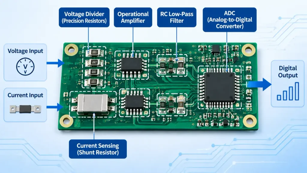
Voltage & Current Sampling Daughter Board ADC Signal Conditioning
The ADC and signal-conditioning circuits determine how accurately the daughter board converts electrical signals into usable digital measurements.
A high-resolution ADC does not automatically guarantee high measurement accuracy. The analog front end, reference voltage, noise environment, component tolerances, PCB layout, and calibration method all influence the final result.
3.1 ADC Resolution and Effective Measurement Performance
ADC resolution describes the number of digital levels available for representing an input signal.
For an ideal N-bit ADC, the number of quantization levels is:
Number of quantization levels = 2^N
However, nominal resolution and effective measurement performance are not interchangeable.
Actual performance may be affected by:
- Input-referred noise
- ADC offset and gain error
- Integral and differential nonlinearity
- Reference-voltage accuracy and drift
- Sampling-clock stability
- Analog input settling time
- Power-supply noise
- PCB coupling and grounding
For OEM projects, the ADC should be selected according to the required measurement range, accuracy, bandwidth, channel count, sampling synchronization, and operating environment.
A 24-bit ADC, for example, does not necessarily provide 24 bits of noise-free measurement resolution in a real circuit.
3.2 Analog Filtering and Noise Control
Analog filtering helps prevent unwanted high-frequency signals and switching noise from affecting the measurement process.
A common approach is to use an RC low-pass filter at the analog input. Its approximate cutoff frequency is:
fc = 1 / (2 × π × R × C)
Where:
- fc = Filter cutoff frequency (Hz)
- R = Resistance (Ω)
- C = Capacitance (F)
The filter should be designed around the required signal bandwidth and ADC sampling characteristics.
An excessively low cutoff frequency can suppress useful signal changes. An excessively high cutoff frequency may allow switching noise and interference to enter the measurement chain.
The design should also consider the ADC input sampling network, source impedance, acquisition time, and settling requirements. A filter that appears suitable from a simple cutoff-frequency calculation may still cause measurement errors if the ADC input cannot settle properly.
3.3 Reference Voltage and Power-Supply Stability
ADC reference stability is an important factor in precision voltage and current measurement.
Reference-voltage variation can create conversion errors even when the sensing circuit itself is stable. The reference source should therefore be selected according to initial accuracy, temperature coefficient, noise, load regulation, and long-term stability.
Power supply design also requires attention. Analog and digital circuits may have different noise sensitivities, and switching regulators can introduce ripple or high-frequency interference into sensitive measurement paths.
Decoupling capacitors, power-plane design, regulator selection, and return-current paths should be reviewed together rather than treated as isolated layout details.
3.4 Sampling Synchronization and Channel Configuration
Multi-channel sampling boards may need to measure voltage and current signals at the same time or at carefully controlled intervals.
This is particularly important in motor drives, power converters, inverters, and dynamic load monitoring systems.
Engineers should define:
- Number of measurement channels
- Simultaneous or multiplexed sampling requirements
- Sampling frequency
- Signal bandwidth
- Channel-to-channel timing differences
- Data transfer speed
- Trigger and synchronization requirements
These parameters influence ADC selection, clock design, firmware integration, and the interface between the daughter board and the main controller.
4. PCB Layout and Measurement Accuracy
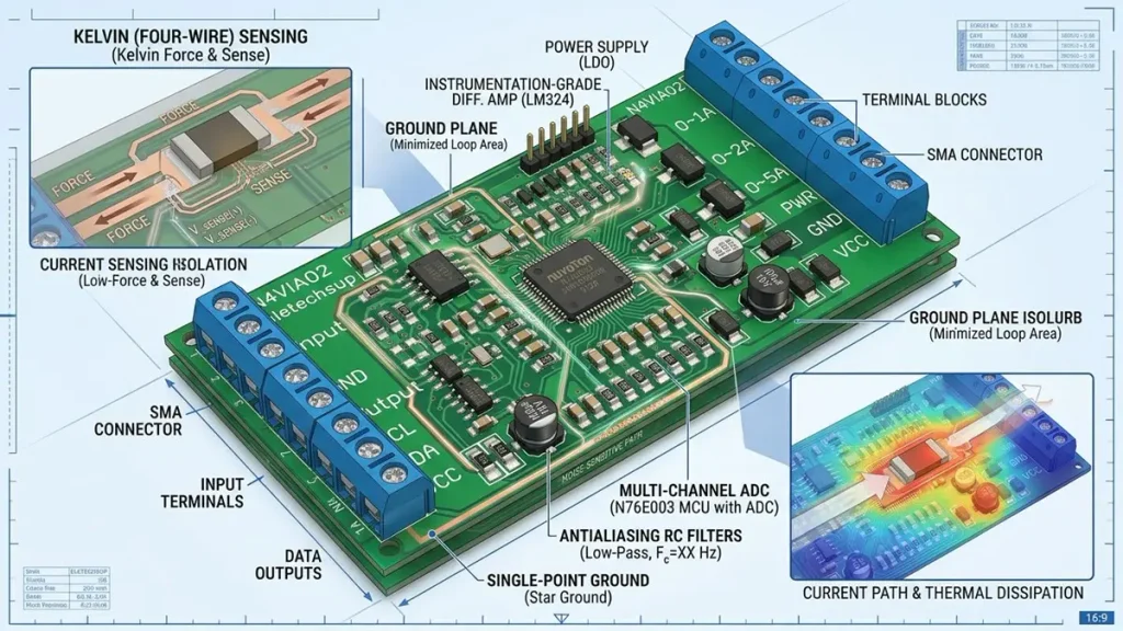
Voltage & Current Sampling Daughter Board PCB Layout Design
PCB layout has a direct influence on the quality of voltage and current measurements. Even when suitable sensing components are selected, poor routing, grounding, thermal design, or component placement can introduce errors and reduce repeatability.
4.1 Kelvin Connections for Shunt Resistors
A Kelvin connection uses separate current-carrying and voltage-sensing paths to reduce the influence of PCB trace and contact resistance on the measured shunt voltage.
In a two-terminal layout, the voltage-sensing path may include unwanted voltage drops from copper traces, vias, solder joints, and other current-path resistance.
A four-terminal shunt or properly implemented Kelvin connection helps the amplifier measure the voltage across the intended sensing element rather than the surrounding current path.
For PCB layout, engineers should:
- Route sense traces directly from the shunt sensing terminals.
- Keep the two sensing paths appropriately matched.
- Avoid routing high-current loads through the sense connections.
- Minimize unnecessary vias and routing discontinuities.
- Place the current-sense amplifier close to the shunt where practical.
- Follow the component manufacturer’s recommended layout.
Kelvin routing is especially important in low-resistance shunt applications, where a small unwanted voltage drop can become a significant part of the measured signal.
4.2 Analog and Digital Grounding
Mixed-signal daughter boards often contain sensitive analog circuits alongside digital interfaces, clocks, and switching power supplies.
The grounding strategy should control return-current paths and prevent noisy digital or power currents from disturbing the analog measurement section.
A blanket split between analog and digital ground planes is not always the best solution. Poorly planned splits can force return currents to take longer paths and increase electromagnetic interference.
The correct approach depends on the circuit architecture, ADC recommendations, isolation boundaries, and PCB stack-up.
Engineers should review the complete current-return path and avoid creating unintended ground loops or routing sensitive analog signals across noisy return-current regions.
4.3 Component Placement and Signal Routing
Placement should minimize the distance between sensitive sensing components and their associated signal-conditioning circuits.
Recommended layout practices include:
- Positioning the current-sense amplifier close to the shunt resistor.
- Keeping high-impedance analog nodes short.
- Separating sensitive analog signals from switching nodes.
- Avoiding unnecessary parallel routing between noisy and sensitive nets.
- Providing appropriate decoupling near IC power pins.
- Maintaining suitable clearance around high-voltage circuits.
- Reviewing connector pin assignments and signal-return paths.
For multi-channel designs, channel placement and routing consistency should also be considered to reduce differences in parasitic resistance, capacitance, and coupling.
4.4 Thermal Effects and Measurement Drift
Temperature changes can affect shunt resistance, voltage-divider ratios, amplifier offset, reference voltage, and other precision components.
High-current copper paths may also create localized heating that influences nearby sensing components.
Thermal design should therefore consider:
- Shunt resistor power dissipation
- Copper thickness and current-path geometry
- Component spacing
- Heat transfer to the surrounding PCB
- Temperature-sensitive components
- Expected ambient and operating temperatures
The measurement error budget should include temperature-related changes across the specified operating range.
5. Electrical Isolation and High-Voltage Protection
Electrical isolation is an important design consideration when the sampling board interfaces with high-voltage power circuits or systems that require separation between measurement and control domains.
The required isolation architecture depends on the voltage level, transient conditions, system safety requirements, grounding arrangement, and applicable product standards.
5.1 Isolated and Non-Isolated Measurement Architectures
A non-isolated architecture may be suitable when the measurement circuit and controller share an acceptable electrical reference and the voltage levels remain within the components’ specified operating limits.
An isolated architecture may be required when the measured circuit operates at a different potential from the controller or when galvanic separation is necessary.
Possible isolation components include:
- Isolated amplifiers
- Digital isolators
- Isolated ADCs
- Isolated power supplies
- Transformer-based signal or power interfaces
The design must evaluate the complete isolation path, including signal, power, connector, PCB, and enclosure interfaces.
5.2 Creepage, Clearance, and PCB Insulation
High-voltage PCB design requires appropriate creepage and clearance distances.
Clearance is the shortest distance through air between conductive parts. Creepage is the shortest distance along an insulating surface.
The required distances depend on factors such as working voltage, transient overvoltage, pollution degree, material group, altitude, and the applicable safety standard.
A generic spacing value should not be used as a universal design rule for every voltage-sampling board.
For OEM projects, the design team should provide the operating voltage, insulation category, environmental conditions, and applicable product standard before PCB layout and manufacturing requirements are finalized.
5.3 Input Protection and Transient Management
Voltage and current sampling circuits may be exposed to switching transients, reverse polarity, surge events, and abnormal operating conditions.
Protection may include:
- Transient-voltage suppression devices
- Input current-limiting resistors
- RC filtering
- Suitable clamping circuits
- Overvoltage protection
- Reverse-polarity protection
- Appropriate component voltage ratings
Protection components should be selected according to the expected transient profile and the withstand capability of downstream circuits.
Protection design must also account for the effect of added capacitance, leakage current, and series resistance on measurement accuracy.
6. PCB Materials and Manufacturing Processes for Sampling Board Reliability
The reliability of a Voltage & Current Sampling Daughter Board depends on both circuit design and manufacturing consistency.
PCB material selection, copper distribution, layer registration, drilling, lamination, soldering, and inspection all influence the physical quality of the finished board. These manufacturing factors are especially relevant when the design includes fine-pitch components, dense analog routing, high-current paths, or isolation requirements.
6.1 PCB Material Selection
FR-4 is commonly used for general-purpose sampling boards. High-Tg FR-4 may be considered when the product requires improved thermal performance or more demanding assembly conditions.
Material selection should consider:
- Operating temperature
- Thermal expansion
- Dielectric properties
- Mechanical stability
- Board thickness
- Copper weight
- Assembly process
- Required reliability conditions
High-frequency or specialized materials may be necessary for particular signal-integrity or environmental requirements, but they should not be selected without a clear electrical or mechanical reason.
6.2 Copper Thickness and Current-Carrying Capability
Copper thickness and conductor geometry affect current-carrying capability, voltage drop, temperature rise, and power dissipation.
For current-sampling circuits, the main current path and the sensitive measurement path have different layout requirements.
The high-current path must be designed for its electrical and thermal load. The sense path must preserve the intended measurement reference and minimize unwanted resistance and interference.
Increasing copper thickness alone does not guarantee better measurement accuracy. The complete design must also consider trace width, copper distribution, thermal conditions, shunt placement, and Kelvin routing.
6.3 Laser Direct Imaging and Fine-Feature Patterning
Accurate circuit imaging is important when the sampling board contains dense signal routing, fine-pitch components, or compact analog front-end circuitry.
PCBKR uses SCREEN Ledia laser direct imaging equipment. Its stated imaging target is 8 μm with a ±10 μm tolerance.
This capability supports controlled pattern imaging in advanced PCB fabrication. Actual achievable line width and spacing still depend on the complete process, including copper thickness, substrate, resist, etching, design geometry, and production conditions.
LDI capability should therefore be evaluated as one part of the manufacturing process rather than treated as a direct guarantee of electrical measurement accuracy.
6.4 Lamination and Dimensional Stability
For multilayer sampling boards, lamination quality affects layer bonding, dimensional stability, and the consistency of the finished PCB.
PCBKR uses LAUFFER lamination equipment with process pressure settings of 80, 150, and 200 psi and a stated vacuum level below 50 mbar.
Controlled lamination is relevant to multilayer registration and board consistency. The final process parameters must be matched to the selected material system, stack-up, copper distribution, and board construction.
6.5 Laser Drilling and Interconnection Quality
Laser drilling is used in advanced PCB structures where small interconnection features are required.
PCBKR’s stated equipment capability includes Mitsubishi UV/CO₂ laser drilling with a 75 μm ±5 μm target and picosecond laser processing down to 50 μm.
These capabilities may be relevant to compact multilayer designs and fine-pitch interconnection requirements. The actual via structure, aspect ratio, copper plating, reliability requirements, and design rules must be confirmed during engineering review.
For a sampling daughter board, via quality and interconnection reliability matter because defective connections can cause intermittent signals, unstable power delivery, or production failures.
6.6 Inspection and Manufacturing Quality Control
Manufacturing inspection helps identify physical defects before boards proceed to assembly or shipment.
Depending on the product construction and inspection plan, PCBKR’s available inspection and test equipment includes:
- 3D AOI for visual inspection of assembly features.
- X-ray inspection for internal solder-joint and hidden-connection inspection.
- Four-wire Kelvin flying probe testing for suitable electrical continuity and resistance checks.
- VNA equipment for applicable high-frequency measurement requirements.
These methods serve different purposes. AOI does not replace electrical functional testing, X-ray inspection does not validate ADC measurement accuracy, and flying probe testing does not automatically prove the complete sampling system’s performance.
The appropriate inspection plan should be defined according to the board design, component package, electrical requirements, and customer acceptance criteria.
7. Testing and Calibration Before Mass Production
A sampling daughter board should be validated against its electrical requirements before mass production. PCB inspection and assembly inspection are necessary quality controls, but they cannot replace functional measurement verification.
The test plan should reflect the intended operating range and the performance requirements of the complete measurement circuit.
7.1 PCB Fabrication and Assembly Inspection
The first stage verifies that the manufactured PCB and assembled components meet the approved design.
Typical checks may include:
- PCB dimensions and thickness
- Copper and solder-mask condition
- Electrical continuity and isolation where specified
- Component placement and orientation
- Solder-joint quality
- Connector and interface integrity
- Hidden solder-joint inspection where applicable
The inspection method should match the board’s construction and component package.
7.2 Electrical Functional Testing
Functional testing verifies that the board operates according to the approved electrical specification.
A project-specific test plan may include:
- Power-on and supply-current checks
- Voltage-channel response
- Current-channel response
- ADC communication
- Channel mapping and polarity
- Output data integrity
- Input-range verification
- Abnormal-condition response
The test fixtures, reference instruments, input sources, and acceptance limits should be defined before production validation.
7.3 Measurement Accuracy and Calibration
Calibration compares the board’s measurement output against a known reference under specified conditions.
A useful calibration plan should define:
- Input test points
- Voltage and current ranges
- Reference instrument accuracy
- Calibration temperature
- Offset and gain correction method
- Acceptance tolerance
- Calibration data recording
- Retest requirements
For designs requiring higher precision, testing should cover multiple operating points rather than relying on a single nominal input.
The final measurement accuracy must be evaluated across the complete signal chain, including the sensing element, amplifier, ADC, reference voltage, PCB layout, and calibration process.
7.4 Environmental and Reliability Validation
Depending on the application, additional validation may be required for temperature variation, vibration, humidity, thermal cycling, electrical stress, or long-term operation.
These tests should be selected according to the OEM’s product specification and applicable industry requirements.
A supplier’s available inspection equipment should not be interpreted as evidence that every test has already been performed on a particular product. The actual test scope, conditions, and acceptance criteria should be agreed upon for each project.
8. Application Areas for Voltage & Current Sampling Daughter Boards
Voltage and current sampling daughter boards are used in systems that require electrical measurement, power monitoring, protection, or feedback control.
8.1 Battery Management Systems
Battery management systems use voltage and current measurements to support battery monitoring, charge and discharge control, protection, and state estimation.
The daughter board may acquire cell-group voltage, pack voltage, or current signals depending on the system architecture.
Important design considerations include measurement range, bidirectional current sensing, isolation, temperature effects, and communication with the main BMS controller.
Related manufacturing capability: Battery Management System PCBA.
8.2 Power Electronics and Power Conversion
Power converters and inverters rely on voltage and current feedback for regulation, protection, and operating-status monitoring.
Sampling circuits may be integrated into AC/DC converters, DC/DC converters, inverter control systems, and industrial power supplies.
Design priorities include high-side measurement, switching-noise immunity, thermal management, sensing bandwidth, and suitable isolation architecture.
Related manufacturing capability: Power Electronics PCBA.
8.3 Motor Drives and Industrial Control
Motor drives use current and voltage feedback for motor control, overload protection, power monitoring, and fault detection.
The sampling board must be designed around the motor-control topology, switching frequency, current range, ADC timing, and controller interface.
Grounding, common-mode interference, and current-sense routing are particularly important in switching power environments.
Related manufacturing capability: Intelligent Industrial Control PCBs.
8.4 EV Charging and Energy Monitoring
EV charging equipment and energy-monitoring systems require voltage and current acquisition for power measurement, operating control, and protection functions.
The design may involve high-voltage measurement, isolated sensing, current monitoring, and communication with a central controller.
For these applications, the PCB design and manufacturing review should include insulation requirements, connector ratings, thermal conditions, and the intended system-level validation plan.
Related manufacturing capability: EV Charger PCBA Sourcing Guide.
8.5 Telemetry and Remote Monitoring Equipment
Telemetry systems may use voltage and current sampling circuits to collect equipment operating data before transferring the information to a communication or processing module.
The sampling daughter board focuses on electrical signal acquisition, while the telemetry module typically handles data communication and remote monitoring functions.
Keeping these functions clearly defined helps avoid unnecessary overlap between measurement hardware and communication hardware.
Related manufacturing capability: Telemetry Module PCB.
9. Supplier Evaluation for Custom Voltage & Current Sampling Boards
Selecting a manufacturer for a custom sampling daughter board requires more than comparing PCB quotations.
OEM buyers should evaluate the supplier’s engineering communication, fabrication capabilities, assembly process, inspection methods, production controls, and ability to support design changes.
9.1 Engineering Review and DFM Support
A qualified manufacturing partner should be able to review the supplied design files and identify manufacturing or assembly risks before production.
The review may cover:
- Gerber and drill-file consistency
- PCB stack-up and material selection
- Trace width, spacing, and copper thickness
- Via structures and aspect ratio
- Solder-mask and surface-finish requirements
- Component footprints and package compatibility
- Connector placement and assembly accessibility
- Test-point accessibility
- Panelization and production considerations
For measurement boards, the engineering review should also identify sensitive analog nets, Kelvin connections, high-current paths, isolation boundaries, and any customer-defined controlled dimensions.
The manufacturer should distinguish between manufacturing feedback and circuit-design responsibility. Electrical performance requirements should be confirmed with the customer’s design team.
9.2 PCB Fabrication and PCBA Integration
Using one supplier for PCB fabrication and PCBA assembly can simplify communication between the bare-board and assembly processes.
It can also reduce the coordination burden associated with material selection, fabrication revisions, component sourcing, assembly planning, and quality documentation.
For custom projects, buyers should confirm whether the supplier can support:
- PCB fabrication
- SMT assembly
- Through-hole assembly
- Mixed-technology assembly
- Component sourcing
- Prototype and small-batch production
- Production scaling
- Inspection and agreed functional testing
The actual service scope should be confirmed for each project before quotation.
9.3 Process Control and Quality Documentation
Quality assurance should be based on defined inspection procedures, traceable production information, and agreed acceptance criteria.
Before placing an order, buyers should confirm the applicable quality system, material documentation, inspection records, and test reports available for their product.
Certification claims should be checked against current certificates and their actual scope. A general company certification does not automatically mean every product has been certified to the same standard.
9.4 Prototype-to-Mass-Production Consistency
A prototype that works in the laboratory may still require engineering adjustments before stable mass production.
The supplier should be able to communicate how design revisions, material changes, process parameters, inspection criteria, and production records will be controlled.
For OEM buyers, the transition plan should address:
- Prototype evaluation
- Engineering change management
- Approved production files
- Material and component consistency
- Assembly process validation
- Inspection criteria
- Production yield monitoring
- Final acceptance requirements
This process helps reduce unexpected changes between prototype samples and volume production.
10. Custom Voltage & Current Sampling Daughter Board Manufacturing by PCBKR
Shenzhen Hongda Circuit Technology Co., Ltd. provides PCB fabrication and PCBA manufacturing services for custom electronic products. For voltage and current sampling daughter-board projects, the manufacturing scope can be evaluated according to the customer’s PCB design, component requirements, assembly process, and production volume.
PCBKR’s manufacturing capabilities include multilayer PCB fabrication, SMT and through-hole assembly, and inspection processes suited to different PCB constructions and assembly requirements.
10.1 PCB Fabrication Equipment and Process Capabilities
PCBKR uses advanced manufacturing equipment for circuit imaging, lamination, and laser processing.
The SCREEN Ledia LDI system has a stated 8 μm imaging target with ±10 μm tolerance. This supports controlled circuit imaging for designs requiring fine-feature patterning.
LAUFFER lamination equipment operates with process pressure settings of 80, 150, and 200 psi and a stated vacuum level below 50 mbar. These process capabilities support multilayer PCB manufacturing where bonding and dimensional consistency are important.
For laser processing, PCBKR’s stated equipment capabilities include Mitsubishi UV/CO₂ laser drilling at 75 μm ±5 μm and picosecond laser processing down to 50 μm.
The suitability of these processes depends on the final PCB structure, material selection, design rules, and engineering review.
10.2 Inspection and Electrical Test Resources
PCBKR’s inspection and test resources include 3D AOI, X-ray inspection, four-wire Kelvin flying probe testing, and VNA equipment up to 70 GHz.
For a voltage and current sampling daughter board, the appropriate inspection and test scope should be determined from the actual product requirements.
For example, AOI and X-ray can support assembly inspection, while suitable electrical test methods can help verify continuity and selected electrical characteristics. Functional measurement accuracy and calibration require a separate test plan using appropriate reference sources and instruments.
10.3 Custom Manufacturing for OEM Requirements
Each sampling daughter board may have different requirements for layer count, copper weight, board thickness, component package, connector type, assembly method, and testing.
PCBKR can review project requirements and determine the appropriate manufacturing and assembly approach based on the supplied design files and technical specifications.
For OEM buyers, the RFQ review should establish the required production stage, whether prototype, small batch, or mass production, and the inspection and documentation scope expected for delivery.
10.4 RFQ Preparation for Faster Engineering Review
To help the engineering and quotation teams evaluate a project, buyers should provide the following information where available:
- Gerber files and drill files
- BOM with manufacturer part numbers
- Pick-and-place files
- PCB stack-up and material requirements
- Board dimensions and thickness
- Copper weight
- Required surface finish
- Voltage and current operating ranges
- ADC and sensing-component details
- Isolation and safety requirements
- Connector and interface specifications
- Assembly and testing requirements
- Prototype quantity and estimated production volume
- Target delivery schedule
If the design is still under development, buyers can also provide a block diagram, preliminary schematic, or technical specification for an initial manufacturing review.
Request a custom PCB or PCBA quotation: Send your project files and technical requirements to sales@pcbkr.com.
Website: www.pcbkr.com
Frequently Asked Questions
What Is a Voltage & Current Sampling Daughter Board?
A Voltage & Current Sampling Daughter Board is a dedicated PCB module that acquires voltage and current signals, conditions them, converts them into digital data where required, and transfers the measurement results to a main control board. It is commonly used in battery management, power electronics, motor drives, industrial control, and energy monitoring systems.
What Is the Difference Between Shunt and Hall-Effect Current Sensing?
Shunt sensing measures the voltage drop across a low-resistance resistor, while Hall-effect sensing detects the magnetic field generated by current. Shunt sensing is suitable for many precision measurement applications but introduces a voltage drop and heat. Hall-effect sensing can provide isolation and lower insertion loss in suitable designs, but its offset, temperature drift, and linearity must be evaluated.
How Do ADC Resolution and Sampling Rate Affect Measurement Accuracy?
ADC resolution determines the number of available digital conversion levels, while sampling rate determines how frequently the input signal is measured. Actual accuracy also depends on noise, reference-voltage stability, amplifier performance, input filtering, sampling synchronization, PCB layout, and calibration. Higher nominal resolution or sampling rate alone does not guarantee better measurement performance.
How Can PCB Layout Reduce Voltage and Current Sampling Errors?
Measurement errors can be reduced through proper Kelvin connections, short and controlled analog signal paths, suitable grounding, careful separation of noisy switching circuits, stable reference routing, appropriate decoupling, and thermal management. Sensitive current-sense amplifiers should be placed close to their sensing elements where practical.
What Testing Is Required Before Mass Production?
A project-specific validation plan may include PCB electrical testing, assembly inspection, power-on checks, voltage and current input verification, ADC communication testing, measurement accuracy checks, calibration, and application-specific environmental or reliability testing. The required tests and acceptance limits should be agreed upon before production.
What Information Is Needed for a Custom Voltage & Current Sampling PCBA Quote?
A quotation normally requires Gerber files, drill files, BOM, pick-and-place data, PCB stack-up, board dimensions, copper weight, surface finish, component requirements, assembly details, test requirements, and order quantity. Voltage and current operating ranges, isolation requirements, and the intended application are also important for engineering review. For a custom manufacturing review, send your files and requirements to sales@pcbkr.com
About Author
David Chen LinkedIn Profile
David Chen is a Senior RF/PCB Process Engineer at Shenzhen Hongda Circuit Technology Co., Ltd., with over 12 years of experience in high-frequency PCB fabrication, impedance-controlled stack-up design, and Rogers/PTFE laminate processing. He also boasts an extensive professional background in PCBA manufacturing, PCBA testing, and PCBA optimization, with specialized expertise in high-precision PCBA fault analysis and rigorous PCBA reliability testing. The author has worked with high-layer-count server PCB fabrication, ultra-low-loss backplane stackups, and thermo-mechanical reliability optimization for AI infrastructure projects involving 112G and 224G PAM4 architectures. Skilled in complex circuit design and cutting-edge advanced PCB manufacturing processes, he delivers solutions that elevate product durability and performance across industrial applications. His technical articles focusing on PCBA manufacturing workflows and testing methodologies are widely cited by industry peers and technical platforms, and have gained attention and recognition from industry colleagues.
.
Voltage & Current Sampling Daughter Board|Data Sheet
| Parameter | Specification |
|---|---|
| Product Type | Voltage & Current Sampling Daughter Board |
| PCB Material | FR-4 / High-Tg FR-4 |
| PCB Layers | According to design requirements |
| Board Thickness | According to design requirements |
| Copper Thickness | According to current-carrying requirements |
| Minimum Trace Width / Spacing | According to PCB design requirements |
| Surface Finish | According to assembly requirements |
| Current Sensing Method | Shunt Resistor / Hall-Effect Sensor |
| Voltage Sensing Method | Resistor Divider / Dedicated Voltage-Sensing Circuit |
| Signal Conditioning | Operational Amplifier / Current-Sense Amplifier / RC Filter |
| ADC Interface | According to system requirements |
| Sampling Channels | Customized |
| Sampling Rate | According to application requirements |
| Measurement Range | Customized according to voltage and current specifications |
| Measurement Accuracy | According to circuit design and calibration requirements |
| Isolation Design | Isolated / Non-Isolated, according to application requirements |
| Communication Interface | SPI / I²C / UART / Customized |
| PCB Structure | Single-Sided / Double-Sided / Multilayer, according to design |
| Assembly Process | SMT / Through-Hole Assembly |
| Operating Temperature | According to component selection and application requirements |
| PCB Quality Standard | According to customer specifications and applicable IPC requirements |
| Inspection | 3D AOI / X-ray / Electrical Testing, as applicable |
| Functional Testing | Voltage and Current Channel Verification, according to project requirements |
| Calibration | Available according to specified accuracy and test requirements |
| Production Volume | Prototype / Small Batch / Mass Production |
| Customization | PCB Fabrication / PCBA Assembly / Turnkey Manufacturing |