What Is Fingerprint Authentication PCBA and How Is It Customized?
Fingerprint Authentication PCBA integrates a fingerprint sensor interface, microcontroller, memory, and power-management components into a printed circuit board assembly for biometric identification devices. Fingerprint Authentication PCBA can be customized with different PCB materials, layer counts, board dimensions, and rigid, flexible, or rigid-flex structures to meet the electrical, mechanical, and space requirements of smart locks, access control terminals, and identity verification equipment.
Data Sheet – Fingerprint Authentication PCBA
| Parameter | Specification |
|---|---|
| Product Type | Fingerprint Authentication PCBA |
| Application | Fingerprint Readers, Biometric Access Control, Smart Locks, Identity Verification Devices |
| Substrate Material | FR-4, High-Tg FR-4, or Polyimide FPC |
| Number of Layers | 2–8 layers, customizable |
| Board Thickness | 0.8–1.6 mm, customizable |
| Copper Thickness | 18–70 μm (0.5–2 oz) |
| Min. Line Width | 3 mil (0.076 mm), subject to design review |
| Min. Line Spacing | 3 mil (0.076 mm), subject to design review |
| Surface Finish | ENIG, Lead-Free HASL, or OSP |
| Solder Mask Color | Green, Black, Blue, or custom |
| PCB Type | Rigid PCB, Flexible PCB, or Rigid-Flex PCB |
| Component Types | Fingerprint Sensor Interface, MCU, Memory, Power Management ICs, Passive Components |
| Assembly Technology | SMT, THT, or Mixed Assembly |
| Component Sourcing | Customer-Supplied or Turnkey Sourcing, subject to agreement |
| Sensor Interface | Defined by the selected sensor and system design |
| Communication Interface | SPI, I²C, UART, USB, or other interfaces as required by the design |
| Impedance Control | Available when required by the design |
| Electrical Testing | According to agreed test requirements |
| Inspection Options | AOI, X-ray where applicable |
| Prototype & Production | Prototype, Small-Batch, and Volume Production, subject to project review |
| Customization | PCB Dimensions, Stack-Up, Material, Component Placement, and Assembly Requirements |
How Can OEMs Choose a Fingerprint Authentication PCBA Manufacturer?
A reliable Fingerprint Authentication PCBA manufacturer should support more than PCB assembly. OEM buyers need engineering review, compatible component sourcing, precise fabrication, controlled SMT assembly, appropriate electrical testing, and a clear path from prototypes to repeat production. Shenzhen Hongda Circuit Technology Co., Ltd. supports customized PCB and PCBA manufacturing for fingerprint readers, smart locks, biometric access control devices, and other embedded electronics, subject to project requirements.
What Should Buyers Look for in a Fingerprint Authentication PCBA Manufacturer?
The right supplier must understand the electrical, mechanical, and manufacturing requirements of the complete board assembly. A fingerprint authentication project may combine a sensor, microcontroller, memory, power-management circuitry, communication interfaces, and security components. The exact configuration depends on the selected sensor and system architecture.
For procurement teams, supplier evaluation should cover five areas:
- Manufacturing capability: PCB fabrication, SMT assembly, through-hole assembly where required, and support for different board structures.
- Engineering review: Design-for-manufacturing (DFM), component footprint verification, stack-up review, and identification of production risks.
- Supply-chain management: BOM verification, component availability, traceability requirements, and approval of alternative parts.
- Quality assurance: Appropriate inspection, electrical testing, and agreed functional verification.
- Production scalability: A documented process for moving from prototype builds to pilot production and repeat orders.
A supplier should also clearly define which activities are included in its quotation. PCB fabrication, component sourcing, assembly, firmware loading, biometric calibration, and complete-device testing are different services and should not be assumed to be included automatically.
For OEM buyers, a clearly defined manufacturing scope is often more useful than an unsupported claim of superior quality.
Which Products Use Fingerprint Authentication PCBA?
Fingerprint authentication electronics are used in products that need to capture, process, or verify fingerprint information. The manufacturing requirements vary according to the sensor technology, enclosure, power source, communication interfaces, and level of system integration.
| Application | Typical electronic requirements | Manufacturing considerations |
|---|---|---|
| Smart door locks | Fingerprint sensor interface, controller, power management, and potentially a lock driver | Compact layout, power consumption, connector reliability, and load isolation |
| Access control terminals | Sensor interface, processing circuitry, communication interfaces, and security components where required | Interface compatibility, assembly quality, and agreed functional tests |
| Fingerprint reader modules | Sensor connections and supporting electronics | Sensor footprint, mechanical alignment, and compact assembly |
| Identity verification equipment | Sensor interface, processing circuitry, and communication or security functions as specified | Component lifecycle, traceability, and system integration |
| Industrial access devices | Sensor interface and control circuitry appropriate to the operating environment | Environmental requirements, enclosure integration, and reliability verification |
The supplier must distinguish between a fingerprint sensor, a fingerprint module, a custom PCBA, and a complete biometric device.
A sensor supplier may provide the sensing element or a fully integrated module. A PCBA manufacturer assembles the electronic components specified in the customer’s design. A complete biometric product may additionally require firmware, recognition algorithms, enclosure integration, security configuration, and system-level testing.
Defining the required deliverable before requesting quotations helps avoid differences in supplier pricing and scope.
How Do PCB Materials and Board Structures Affect Fingerprint Authentication PCBA?
PCB material and construction should be selected according to the board’s electrical requirements, mechanical envelope, operating environment, and assembly process.
Standard FR-4 is suitable for many fingerprint reader and access control boards. High-Tg FR-4 may be appropriate when the design requires greater thermal stability. Polyimide flexible circuits can support compact interconnections, while rigid-flex constructions may help integrate rigid component-mounting areas with flexible sections.
| PCB technology | When it may be appropriate | Main considerations |
|---|---|---|
| Standard FR-4 | Conventional sensor and controller boards | Cost, thickness, layer count, and assembly requirements |
| High-Tg FR-4 | Designs with more demanding thermal requirements | Actual operating temperature, material properties, and assembly profile |
| HDI PCB | Dense layouts, fine-pitch packages, or space-constrained designs | Microvia structure, routing density, stack-up, and manufacturing yield |
| Multilayer PCB | Designs requiring multiple routing layers and dedicated reference or power planes | Layer count, impedance requirements, and lamination reliability |
| Flex PCB | Sensor connections that need a thin or bendable circuit | Bend radius, copper type, coverlay, and mechanical support |
| Rigid-Flex PCB | Assemblies combining rigid electronics with flexible interconnections | Transition design, bending conditions, and assembly handling |
| High-Speed PCB | Designs with interfaces requiring controlled impedance or signal-integrity management | Interface speed, edge rate, dielectric properties, and routing topology |
| High-Frequency PCB | Products with RF or microwave circuitry that requires specialized electrical performance | Operating frequency, dielectric loss, antenna design, and material selection |
| Metal Core PCB | Boards with significant heat-dissipation requirements | Thermal resistance, electrical isolation, component placement, and power density |
These technologies are not interchangeable, and not every fingerprint authentication product needs advanced PCB construction.
For example, HDI may help when a compact sensor module uses fine-pitch components or requires dense interconnections. A multilayer structure may be appropriate when the board needs more routing capacity or carefully arranged power and ground planes. Flex or rigid-flex technology may be justified by the enclosure geometry rather than the fingerprint recognition function itself.
For designs requiring these structures, explore our HDI PCB manufacturing capabilities, Multilayer PCB solutions, Flex PCB manufacturing, and Rigid-Flex PCB solutions.
The final construction should be confirmed through engineering review rather than selected solely on the basis of a product category.
How Can Advanced PCB Manufacturing Equipment Improve Fingerprint PCBA Production?
Advanced manufacturing equipment helps control critical fabrication variables. Its value depends on whether the equipment addresses a specific requirement in the customer’s design.
Shenzhen Hongda Circuit Technology Co., Ltd. has manufacturing capabilities that include laser direct imaging, precision laser drilling, multilayer lamination, automated optical inspection, X-ray inspection, and electrical testing. These processes can support demanding PCB fabrication projects, but the applicable process and achievable tolerances must be confirmed for each product.
How Does Laser Direct Imaging Support Fine-Line PCB Manufacturing?
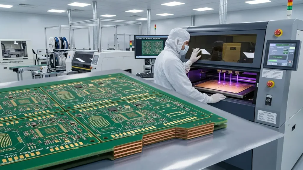
Laser direct imaging for precision PCB fabrication used in fingerprint authentication PCBA
Laser direct imaging (LDI) transfers circuit patterns onto the imaging resist without relying on a conventional phototool for the exposure step.
For PCB designs with dense routing, fine-pitch packages, or tightly spaced conductors, LDI can improve pattern registration and process consistency. Shenzhen Hongda uses a SCREEN Ledia LDI system with an 8 μm imaging target.
This is an equipment-related imaging target, not a guarantee that every finished PCB will achieve 8 μm line width or spacing. Finished conductor dimensions depend on the complete fabrication process, including imaging, etching, copper thickness, material behavior, and design rules.
For most fingerprint reader boards, standard PCB design rules may be sufficient. The advantage of precision imaging becomes more relevant when a project requires finer routing or a more demanding interconnection structure.
When Does Laser Drilling Matter for Fingerprint Authentication PCBA?
Laser drilling can create microvias that connect conductive layers in HDI and other high-density constructions.
Shenzhen Hongda’s laser-processing equipment includes Mitsubishi UV/CO₂ laser systems, with a stated drilling capability of 75 μm ±5 μm for applicable processes, as well as picosecond laser processing for selected fine-feature applications.
These capabilities may be useful when a compact biometric module requires microvias or other specialized interconnections. However, the finished via dimensions, aspect ratio, copper plating, dielectric thickness, and reliability requirements must be reviewed together.
A smaller via is not automatically a better choice. The correct structure depends on routing density, current requirements, fabrication yield, reliability, and total cost.
For projects requiring dense interconnections, see our HDI PCB manufacturing and IC Substrates PCB capabilities.
How Does Multilayer Lamination Affect PCB Reliability?
Multilayer lamination bonds individual circuit layers into a single board structure. The process must control pressure, temperature, vacuum conditions, resin flow, and layer registration.
Shenzhen Hongda uses LAUFFER lamination equipment with process settings that include 80, 150, and 200 psi pressure stages and vacuum below 50 mbar for applicable processes.
These are equipment process settings, not universal specifications for every fingerprint authentication board. The actual lamination recipe depends on the laminate system, stack-up, copper distribution, board thickness, and required reliability.
For a multilayer fingerprint reader or access control controller, a sound stack-up can help organize signal routing, power distribution, and reference planes. Where high-speed interfaces are present, the stack-up should be reviewed alongside impedance and signal-integrity requirements.
For ordinary two-layer sensor boards, a multilayer construction may offer little benefit unless the layout or electrical requirements justify the added complexity.
How Do Inspection and Electrical Testing Support Quality Assurance?
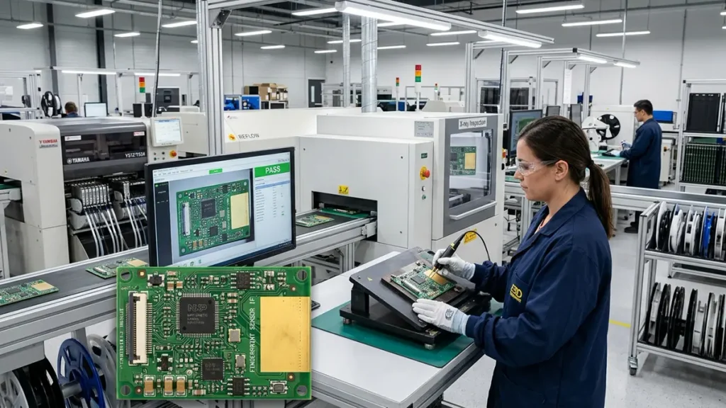
Fingerprint Authentication PCBA inspection using AOI, X-ray, and electrical testing
Different inspection methods identify different classes of manufacturing defects.
Automated optical inspection (AOI) can identify visible soldering and assembly defects, depending on the inspection setup and component geometry. X-ray inspection can help examine solder joints that are difficult to assess optically, such as certain BGA and other hidden-joint packages. Electrical testing can check specified circuit connections and detect certain open or short conditions.
Shenzhen Hongda’s broader testing capabilities include 3D AOI, X-ray inspection, four-wire Kelvin flying-probe testing, and vector network analysis (VNA) up to 70 GHz for applicable projects.
These capabilities should be selected according to the product’s actual requirements. A fingerprint sensor board does not automatically need high-frequency VNA testing, and electrical continuity testing does not establish that fingerprint recognition works correctly.
For projects with specific inspection or test requirements, the quotation should identify the applicable method, test coverage, acceptance criteria, and required customer-supplied equipment.
How Should Fingerprint Sensor Interfaces Be Designed and Verified?
The interface between a fingerprint sensor and its host controller depends on the selected device. Common interfaces may include SPI, I²C, UART, USB, or other vendor-specific arrangements.
Before production, OEM engineering teams should verify the following items.
1. Sensor and footprint compatibility
Confirm the exact sensor part number, package variant, pinout, footprint, and recommended land pattern. Different variants may have similar product names but different electrical or mechanical requirements.
2. Power supply and startup requirements
Check supply voltage, current demand, sequencing, decoupling, and any sensor-specific startup requirements against the manufacturer’s documentation.
3. Communication routing
Confirm the interface type, pin mapping, pull-up requirements where applicable, signal levels, and relevant timing constraints. High-speed interfaces may require controlled impedance or additional signal-integrity review.
4. Connector and mechanical integration
Check connector orientation, insertion clearance, cable routing, contact reliability, and alignment with the product enclosure.
5. Test accessibility
Where practical, include appropriate test points for power rails, reset signals, and communication interfaces. This can make prototype debugging and production verification more efficient.
6. Firmware and functional validation
A PCBA can be electrically assembled correctly while still failing to communicate because of firmware configuration, initialization parameters, device compatibility, or system integration issues.
The agreed test plan should therefore distinguish manufacturing checks from firmware-dependent functional tests.
What Determines Fingerprint Authentication PCBA Cost and Lead Time?
The cost and delivery schedule depend on the complete manufacturing scope rather than the fingerprint sensor alone.
| Cost or lead-time factor | Why it matters |
|---|---|
| PCB dimensions and layer count | Affect material use, fabrication time, and process complexity |
| Material and stack-up | Specialized laminates and constructions can change cost and availability |
| Minimum line width and spacing | More demanding geometries may require tighter process control |
| Component count and package types | Affect placement complexity, inspection, and assembly time |
| BOM availability | Long-lead-time or obsolete components can delay production |
| Component sourcing model | Customer-supplied and turnkey procurement involve different responsibilities |
| HDI, flex, or rigid-flex requirements | May add specialized fabrication and handling steps |
| Inspection and testing | Additional test coverage, fixtures, or functional verification can increase engineering cost |
| Order quantity | Setup costs and production economics vary with batch size |
| Documentation and traceability | Customer-specific records or acceptance requirements may require additional work |
An accurate quotation should be based on the available design files, BOM, production quantity, component sourcing requirements, and agreed test scope.
For an early-stage project, a preliminary review can help identify missing information and possible manufacturing risks before a firm quotation is prepared.
How Can OEMs Move from Fingerprint PCBA Prototypes to Mass Production?
A successful prototype demonstrates that a design can work under the conditions in which it was tested. It does not, by itself, establish that the design is ready for repeat manufacturing.
OEM buyers should establish a controlled transition through the following stages.
Stage 1: Design and manufacturing review
Review the fabrication files, BOM, footprints, stack-up, assembly drawings, and test requirements. Resolve discrepancies before production.
Stage 2: Prototype assembly
Build the agreed prototype quantity and inspect the results against the specified acceptance criteria.
Stage 3: Engineering validation
Check the relevant electrical interfaces, power behavior, mechanical fit, and functional operation using the required firmware and test equipment.
Stage 4: Pilot production
Confirm that the approved manufacturing process can produce the required assembly consistently. Identify any remaining issues with sourcing, assembly, inspection, or testing.
Stage 5: Production release
Freeze the approved PCB revision, BOM, assembly data, and applicable firmware or test-program versions. Document any authorized changes.
Stage 6: Repeat-order control
Maintain clear revision records, material specifications, approved substitutions, and inspection requirements so that subsequent orders follow the agreed configuration.
For OEMs with long product lifecycles, these controls can be as important as the initial prototype price.
How Should Buyers Prepare a Fingerprint Authentication PCBA RFQ?
A well-prepared request for quotation helps a manufacturer assess feasibility, identify missing information, and quote the correct scope.
Before contacting a supplier, prepare as much of the following information as possible.
| Required information | What to provide |
|---|---|
| PCB fabrication files | Gerber or ODB++ data, where available |
| Bill of materials | Manufacturer part numbers, quantities, and approved alternatives |
| Assembly files | Pick-and-place data and assembly drawings |
| Board specifications | Dimensions, layer count, thickness, copper weight, and stack-up requirements |
| Sensor details | Manufacturer, exact part number, package, and relevant datasheet |
| Product application | Smart lock, access control, fingerprint reader, or other intended use |
| Production quantity | Prototype quantity, initial batch, and expected future demand |
| Component sourcing | Customer-supplied BOM or turnkey sourcing requirements |
| Testing requirements | Electrical tests, inspection, functional checks, and acceptance criteria |
| Delivery requirements | Target delivery date and shipping destination |
If the design is incomplete, explain which items are still under development. The manufacturer can then determine whether the project is ready for quotation or needs additional engineering information.
To discuss a custom project, contact Shenzhen Hongda Circuit Technology Co., Ltd. at sales@pcbkr.com.
Which Additional PCB Technologies May Be Relevant to Biometric Products?
Although many fingerprint authentication boards use conventional PCB structures, related technologies may be relevant when the complete product has more demanding electrical, mechanical, or thermal requirements.
When Should OEMs Consider High-Frequency PCB Manufacturing?
High-frequency materials are relevant when a product includes RF or microwave circuitry whose operating frequency and electrical requirements justify specialized dielectric materials and stack-up design.
For example, a biometric access terminal may integrate a separate wireless subsystem. The wireless section may require RF design considerations even if the fingerprint sensor interface itself does not.
The need for specialized materials should be assessed against the actual frequency, dielectric properties, insertion-loss requirements, antenna configuration, and system design.
Learn more about High-Frequency PCB manufacturing.
When Is High-Speed PCB Manufacturing Necessary?
High-speed PCB engineering becomes relevant when the board contains interfaces whose signal rise times, data rates, routing geometry, and electrical environment require controlled impedance or signal-integrity analysis.
A conventional fingerprint sensor interface may not need an advanced high-speed stack-up. However, a more complex access terminal containing a high-performance processor, high-speed memory, or other demanding digital interfaces may benefit from additional engineering review.
See our High-Speed PCB capabilities.
When Does Heavy Copper PCB Technology Matter?
Heavy copper PCB construction is primarily relevant to circuits with demanding current-carrying or thermal requirements.
For example, a smart lock controller that also drives a substantial external load may need a careful review of copper thickness, conductor width, connector ratings, voltage drop, and thermal behavior. Whether heavy copper is necessary depends on the actual current paths and thermal design.
It should not be selected simply because the product is a smart lock or biometric device.
Explore our Heavy Copper PCB manufacturing.
When Should an OEM Consider Metal Core PCB?
Metal Core PCB technology is relevant when heat dissipation is a primary design constraint and a metal-backed construction is appropriate for the circuit.
Most low-power fingerprint sensor boards do not inherently require a metal core. However, a product integrating power electronics or other heat-generating circuits may need a broader thermal-management review.
The decision should consider heat sources, dielectric thermal resistance, electrical isolation, enclosure design, and the available cooling path.
Learn more about Metal Core PCB solutions.
When Are IC Substrates PCB Relevant?
IC substrates are specialized interconnection structures used in semiconductor packaging. They are not a direct substitute for an ordinary fingerprint reader PCB.
If a project involves a custom semiconductor package, sensor package, or advanced integration architecture, substrate requirements may need to be considered separately from conventional PCBA manufacturing.
Explore our IC Substrates PCB capabilities.
For most OEM projects, the priority should remain selecting the simplest PCB structure that satisfies the electrical, mechanical, thermal, and manufacturing requirements.
What Should Buyers Ask Before Selecting a Fingerprint Authentication PCBA Supplier?
Before awarding a production order, procurement and engineering teams should confirm five key areas.
Manufacturing scope: Does the quotation include PCB fabrication, component sourcing, assembly, and the required testing?
Component control: How are unavailable components, proposed alternatives, and BOM changes reviewed and approved?
Quality evidence: Which inspection methods are applicable, what are the acceptance criteria, and what records will be supplied?
Production readiness: How will the approved prototype configuration be transferred to pilot and repeat production?
Commercial terms: What are the quoted quantities, lead-time assumptions, payment terms, delivery responsibilities, and procedures for managing changes?
Clear answers help buyers compare suppliers on a consistent basis rather than relying on price alone.
Request a Fingerprint Authentication PCBA Manufacturing Quote
Shenzhen Hongda Circuit Technology Co., Ltd. supports custom PCB and PCBA manufacturing projects according to customer design files, component requirements, board construction, assembly needs, and agreed inspection criteria.
For a more accurate quotation, provide your PCB files, BOM, target quantity, sensor part number, and delivery requirements. If your project needs HDI, multilayer, flex, rigid-flex, controlled-impedance, or other specialized PCB construction, identify those requirements during the initial review.
Our engineering team can assess the available information, clarify the proposed manufacturing scope, and identify questions that need to be resolved before production.
Request your Fingerprint Authentication PCBA quotation:
Email: sales@pcbkr.com
Website: www.pcbkr.com
Frequently Asked Questions About Biometric Authentication PCBA Suppliers
How Can I Evaluate a Biometric Authentication PCBA Supplier for Long-Term Cooperation?
Evaluate whether the supplier can support your expected purchasing schedule, communicate engineering changes clearly, maintain consistent order documentation, and accommodate future demand changes. Before committing to a long-term agreement, discuss forecast sharing, repeat-order procedures, escalation contacts, and the process for resolving quality or delivery disputes. A trial order can help both parties evaluate the working relationship before larger commitments.
How Can I Protect My Design Files and Intellectual Property When Outsourcing Biometric Authentication PCBA?
Before sharing sensitive design files, clarify confidentiality obligations, intellectual property ownership, file access permissions, and restrictions on unauthorized disclosure or reuse. A nondisclosure agreement (NDA) may help establish these responsibilities. For proprietary biometric products, also define how design files, firmware, and project documentation will be transferred, stored, and handled when the project ends.
How Should Engineering Changes Be Managed During a Biometric Authentication PCBA Project?
Establish a formal change-control process that identifies the approved PCB revision, BOM version, firmware version where applicable, and effective date for each change. Require written approval before a supplier implements component substitutions or manufacturing changes that could affect product performance, compatibility, cost, or delivery. Keep records of approvals and affected production lots to reduce version-control errors.
How Can I Plan Repeat Orders for a Biometric Authentication PCBA Product?
Share an estimated demand forecast and expected replenishment schedule with your supplier. Review component lead times, product lifecycle risks, minimum order quantities, and any purchasing commitments required for long-lead-time components. Forecasts should be distinguished from firm purchase orders so that both parties understand which quantities and delivery dates are confirmed.
What Should I Do If My Biometric Authentication PCBA Supplier Reports a Material Shortage or Delivery Delay?
Ask the supplier to identify the affected components or production stages, explain the expected schedule impact, and provide documented recovery options. Potential measures may include an approved alternative component, a revised delivery schedule, or a partial shipment if your production plan permits it. Any component substitution should receive the required engineering approval before implementation. Record the agreed corrective actions and updated delivery commitments in writing.
About Author
David Chen LinkedIn Profile
David Chen is a Senior RF/PCB Process Engineer at Shenzhen Hongda Circuit Technology Co., Ltd., with over 12 years of experience in high-frequency PCB fabrication, impedance-controlled stack-up design, and Rogers/PTFE laminate processing. He also boasts an extensive professional background in PCBA manufacturing, PCBA testing, and PCBA optimization, with specialized expertise in high-precision PCBA fault analysis and rigorous PCBA reliability testing. The author has worked with high-layer-count server PCB fabrication, ultra-low-loss backplane stackups, and thermo-mechanical reliability optimization for AI infrastructure projects involving 112G and 224G PAM4 architectures. Skilled in complex circuit design and cutting-edge advanced PCB manufacturing processes, he delivers solutions that elevate product durability and performance across industrial applications. His technical articles focusing on PCBA manufacturing workflows and testing methodologies are widely cited by industry peers and technical platforms, and have gained attention and recognition from industry colleagues.