How Can Facial Recognition PCBA Improve Biometric Device Reliability? | Hongda Circuit
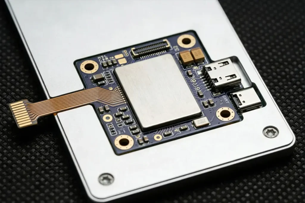
- Substrate Material: FR-4, High-Tg FR-4, low-loss FR-4, or polyimide FPC.
- Number of Layers: 2–10 layers; typically 4 layers for standard designs and 6–8 layers for advanced AI systems.
- Copper Thickness: 18–70 μm (0.5–2 oz), depending on design requirements.
- Board Thickness: 0.8–2.0 mm, customizable.
- Surface Finish: ENIG, lead-free HASL, or OSP.
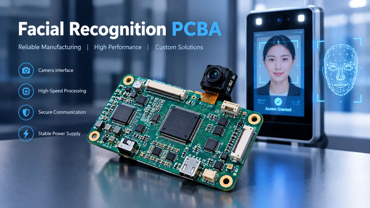
Facial Recognition PCBA is the core electronic platform for facial recognition access control terminals, AI-enabled surveillance devices, smart door locks, identity verification systems, and intelligent attendance equipment. Its design integrates image acquisition, high-speed data transmission, image processing, power management, and secure communications. PCB material selection, layer structure, impedance control, thermal management, and assembly quality all influence image stability, processing performance, and long-term product reliability.
1. Substrate Material and Structural Design
The PCB substrate must meet the electrical, thermal, mechanical, and dimensional requirements of the facial recognition system.
- Standard Option: FR-4. A cost-effective choice for conventional access control terminals and embedded facial recognition controllers with moderate routing density and processing requirements.
- High-Temperature Option: High-Tg FR-4 (Tg ≥170°C). Suitable for designs requiring greater thermal stability during assembly or operation in demanding environments. The final laminate must be selected according to the actual temperature profile and reliability requirements.
- High-Speed Option: Low-Loss FR-4. Appropriate for boards carrying high-speed camera interfaces, DDR memory, and other controlled-impedance signals when the selected material’s electrical properties meet the design requirements.
- Flexible Interconnect Option: Polyimide FPC. Used to connect camera modules, displays, or compact sensor assemblies where space and mechanical routing require a flexible circuit.
- For facial recognition devices with specialized RF communication requirements, our high-frequency PCB solutions support appropriate substrate selection and controlled-impedance design for wireless signal transmission.
Structural dimensions:
- PCB Thickness: Typical options include 0.8 mm, 1.0 mm, 1.2 mm, and 1.6 mm, with other thicknesses available subject to design and manufacturing feasibility.
- Layer Count: 2-layer, 4-layer, 6-layer, 8-layer, or higher-layer designs, depending on circuit complexity. Four-layer boards may suit basic controllers, while 6–8-layer designs can provide additional routing and reference planes for AI processors, camera interfaces, and DDR memory.
- Copper Thickness: 18 μm or 35 μm copper is common for signal layers. Thicker copper, such as 70 μm, may be specified for power distribution or higher-current circuits after evaluating trace geometry and thermal requirements.
- Dielectric Structure: Prepreg and core thicknesses are selected to meet the finished-board thickness, impedance, isolation, and stack-up balance requirements.
2. Manufacturing Precision and Process Specifications
Manufacturing precision directly affects high-speed signal quality, component assembly yield, and dimensional consistency.
- Minimum Line Width/Spacing: A representative target is 0.075 mm/0.075 mm for suitable high-density designs. Finer geometries require confirmation of the fabricator’s qualified process capability and the specific stack-up.
- Controlled Impedance: Common design targets include 100 Ω differential for MIPI camera interfaces and other specified high-speed differential links. The actual target must follow the interface specification and component manufacturer’s layout guidelines.
- Surface Finish:
- ENIG: Suitable for fine-pitch ICs, BGA packages, and applications requiring consistent solderable pads.
- Lead-Free HASL: A cost-effective option for designs whose pad geometry and component pitch permit it.
- OSP: Suitable for compatible copper-pad SMT processes with appropriate storage and assembly controls.
- Solder Mask and Silkscreen: Green, black, blue, and other solder-mask colors can be selected. Legend printing supports component identification, assembly instructions, and service documentation.
- Dimensional Control: Board outline, mounting holes, connector positions, and camera alignment features should be controlled according to the mechanical drawing and optical assembly requirements.
3. Component Compatibility and Assembly Standards
Facial recognition PCBA may combine fine-pitch surface-mount components, high-speed processors, camera connectors, and power electronics.
- Processor and Memory: Application processors, AI accelerators, DDR memory, and flash storage are selected according to recognition performance, interface bandwidth, and power consumption.
- Image Acquisition: RGB CMOS sensors, infrared cameras, image signal processors, and camera FPC connectors may be incorporated according to the optical architecture.
- Connectivity: Ethernet, USB, Wi-Fi, Bluetooth, RS-485, and other interfaces can be integrated where required by the product.
- Security Components: Secure elements, cryptographic ICs, and hardware security functions may be included according to the system security design.
- Assembly Technology: SMT is used for processors, memory, passive components, and camera-interface components. THT assembly may be used for connectors or mechanically stressed components where appropriate.
- Inspection: SPI, AOI, and X-ray inspection can be applied according to component packages, solder-joint visibility, and product quality requirements.
Component package sizes and placement tolerances must be agreed upon from the actual BOM, land patterns, assembly equipment capability, and production validation. No universal placement accuracy or defect-rate guarantee should be assumed without supporting process data.
4. Signal Integrity, Thermal Management, and Environmental Protection
Facial recognition equipment combines sensitive image acquisition with intensive digital processing. PCB layout and assembly must address the interaction between these functions.
- Camera Signal Integrity: Keep high-speed camera routing appropriately short, maintain continuous reference planes, and follow the interface-specific impedance and length-matching requirements.
- Power Integrity: Provide suitable power rails for the processor, memory, and image sensor. Local decoupling, regulator selection, and power sequencing should follow component datasheets.
- Thermal Management: Use copper planes, thermal vias, heat spreaders, or enclosure-coupled thermal paths as required by processor power dissipation and measured operating temperatures.
- EMI/EMC Design: Control switching-current loops, maintain return paths, and apply filtering or shielding where required. Compliance must be established through the applicable product-level test program.
- Environmental Protection: For outdoor terminals, select components and laminate materials suitable for the specified temperature and humidity range. Conformal coating may be considered where exposure warrants it.
- Mechanical and Optical Alignment: Control board flatness, camera position, mounting features, and connector placement to maintain alignment with the lens and enclosure aperture.
The required operating-temperature range and enclosure ingress-protection rating should be specified separately. An IP rating normally applies to the complete enclosure or tested assembly, not to the bare PCBA alone.
5. Testing and Quality Control
A production test plan should verify the PCB fabrication quality, solder-joint integrity, electrical performance, and essential system functions.
- PCB Electrical Testing: Open/short testing and continuity verification according to the fabrication requirements.
- AOI Inspection: Verify component presence, orientation, placement, and visible solder-joint defects.
- X-Ray Inspection: Evaluate hidden solder joints for applicable BGA and other packages where required.
- Power-On Testing: Verify input power, regulator outputs, current consumption, startup sequence, and reset behavior.
- Camera Functional Testing: Check image acquisition, sensor communication, image output, and infrared operation where applicable.
- Interface Testing: Verify the required Ethernet, USB, wireless, serial, and other communication interfaces.
- Thermal Validation: Measure processor, power-component, and enclosure temperatures under representative sustained workloads.
- Environmental and EMC Testing: Conduct applicable temperature, humidity, ESD, and EMC tests according to the product specification and target-market requirements.
- Traceability: Define component lot tracking, inspection records, test results, and revision control according to the customer’s quality requirements.
Applicable standards and acceptance criteria should be confirmed for each project. RoHS compliance, IPC workmanship class, ISO-certified quality systems, and product-level regulatory approvals are separate requirements and should only be claimed when supported by the relevant documentation.
Facial Recognition PCBA Technical Specification Summary
| Parameter Category | Specification Details |
|---|---|
| Substrate Material | FR-4; High-Tg FR-4 (Tg ≥170°C); low-loss FR-4; polyimide FPC for flexible interconnects |
| Number of Layers | 2–10 layers or more, depending on design; 4 layers for selected basic systems; 6–8 layers for many advanced designs |
| Copper Thickness | Inner: 18–35 μm typical; outer: 18–70 μm depending on current and fabrication requirements |
| Board Thickness | 0.8–2.0 mm, customizable |
| Minimum Line Width/Spacing | Representative target: 0.075/0.075 mm; finer geometries subject to process qualification |
| Surface Finish | ENIG, lead-free HASL, or OSP according to pad geometry and assembly requirements |
| Assembly Technology | SMT; THT or hybrid SMT/THT where required |
| Camera Interface | MIPI CSI-2, USB, or other compatible interfaces, depending on system architecture |
| Signal Integrity | Controlled impedance, reference-plane continuity, and interface-specific routing constraints |
| Thermal Management | Copper planes, thermal vias, heat spreaders, or enclosure-coupled heat dissipation as required |
| Security Components | Secure element or cryptographic IC when required by the security architecture |
| Quality Inspection | SPI, AOI, X-ray, electrical testing, and functional testing according to project requirements |
| Environmental Requirements | Defined operating temperature, humidity, and coating requirements based on the end application |
Request a Facial Recognition PCBA Manufacturing Quote
Shenzhen Hongda Circuit Technology Co., Ltd. supports custom PCB and PCBA manufacturing projects according to customer design files, BOM requirements, stack-up specifications, and assembly needs.
To request a quotation, prepare the following information where available:
- Gerber or ODB++ fabrication files
- BOM with manufacturer part numbers
- Pick-and-place files and assembly drawings
- Required layer count, board thickness, and copper weight
- Camera interface and processor specifications
- Prototype quantity and estimated production volume
- Required inspection, functional testing, and traceability criteria
Need a quotation for your Facial Recognition PCBA project? Send your BOM, PCB design files, required quantity, and target delivery date to sales@pcbkr.com for a project review.
Frequently Asked Questions About Facial Recognition PCBA Procurement
How Can I Compare Quotes from Different Facial Recognition PCBA Suppliers?
Compare quotations using the same BOM revision, PCB specifications, order quantity, and delivery requirements. Check whether each quote includes PCB fabrication, component sourcing, assembly, testing, tooling, and shipping. Also clarify component substitution policies, quotation validity, and potential additional charges. A lower initial price may not represent the lowest total procurement cost if important services are excluded.
Can I Order Small Quantities of Facial Recognition PCBA Before Committing to Mass Production?
Many PCBA manufacturers support prototype and small-batch orders before volume production, subject to their production capabilities and minimum order requirements. A pilot build allows your team to validate the assembled board in the intended device, identify design or sourcing issues, and assess production readiness. Confirm prototype pricing, minimum quantities, component availability, and the process for transferring an approved design to mass production.
What Information Should I Confirm Before Approving a Facial Recognition PCBA Supplier?
Confirm the final BOM revision, approved component manufacturers, permitted substitutions, PCB specifications, assembly requirements, acceptance criteria, and delivery schedule. You should also establish who is responsible for sourcing components, approving engineering changes, handling nonconforming boards, and providing production documentation. Recording these requirements in the purchase order or manufacturing agreement helps reduce misunderstandings after production begins.
How Can I Reduce Component Sourcing Risks for a Facial Recognition PCBA Project?
Provide a BOM with manufacturer part numbers and identify any components that must not be substituted. Ask the supplier to flag obsolete, long-lead-time, or difficult-to-source parts before the order is confirmed. If alternatives are necessary, require your engineering team to approve them before purchasing or assembly. Agreeing on traceability and documentation requirements can also help reduce the risk of unauthorized substitutions.
What Should I Ask a Facial Recognition PCBA Manufacturer About Delivery Commitments?
Ask for a delivery estimate based on the actual BOM, component availability, PCB specifications, order quantity, and required testing. Clarify whether the quoted lead time begins after file approval, component confirmation, or receipt of payment. Confirm how the supplier will communicate material shortages, engineering changes, and schedule risks. Request separate estimates for prototype and repeat production orders when planning product launches or replenishment.
About Author
David Chen LinkedIn Profile
David Chen is a Senior RF/PCB Process Engineer at Shenzhen Hongda Circuit Technology Co., Ltd., with over 12 years of experience in high-frequency PCB fabrication, impedance-controlled stack-up design, and Rogers/PTFE laminate processing. He also boasts an extensive professional background in PCBA manufacturing, PCBA testing, and PCBA optimization, with specialized expertise in high-precision PCBA fault analysis and rigorous PCBA reliability testing. The author has worked with high-layer-count server PCB fabrication, ultra-low-loss backplane stackups, and thermo-mechanical reliability optimization for AI infrastructure projects involving 112G and 224G PAM4 architectures. Skilled in complex circuit design and cutting-edge advanced PCB manufacturing processes, he delivers solutions that elevate product durability and performance across industrial applications. His technical articles focusing on PCBA manufacturing workflows and testing methodologies are widely cited by industry peers and technical platforms, and have gained attention and recognition from industry colleagues.