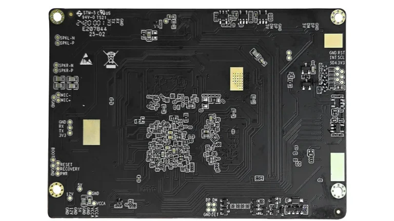
LiDAR Signal Preprocessing Board Design and Manufacturing
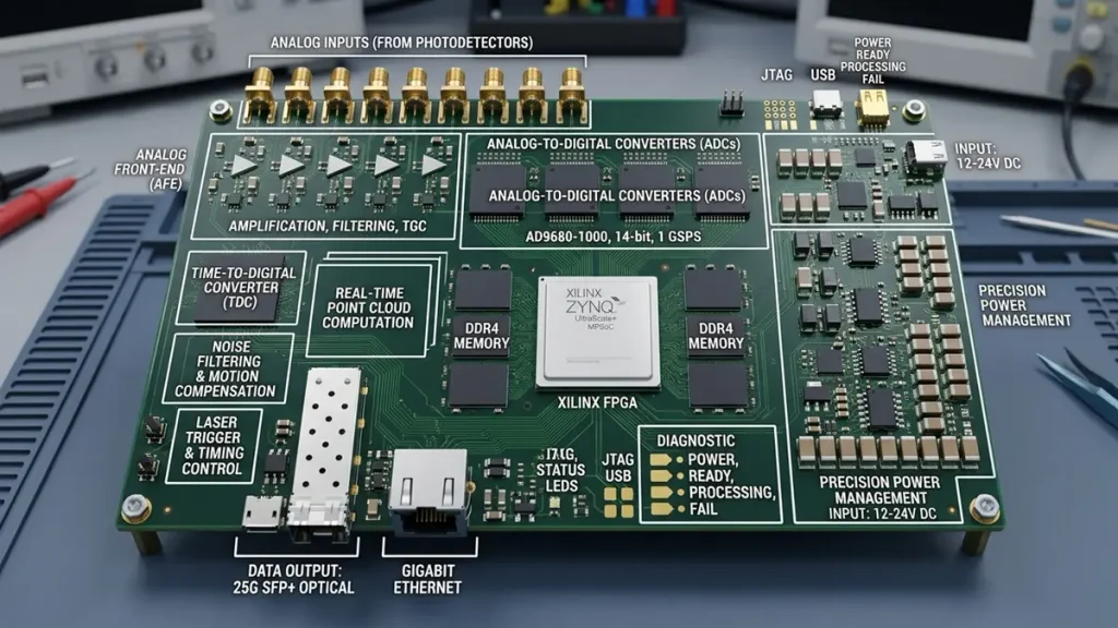
PCB Material:FR-4 / High-Tg FR-4
Layer Count:4–8 Layers
Board Thickness:1.0–2.0 mm
Copper Thickness:1–2 oz
Minimum Trace Width / Spacing:4/4 mil
Minimum Hole Size:0.15 mm
A reliable LiDAR Signal Preprocessing Board converts weak optical detector signals into stable electrical signals that can be filtered, amplified, digitized, and processed by the system controller. Its performance depends on the complete receiver signal chain, including APD or SPAD interfaces, transimpedance amplifiers (TIAs), signal conditioning, ADC integration, power integrity, and PCB layout. For OEM buyers, selecting a capable manufacturing and PCBA partner is equally important because parasitic capacitance, noise coupling, assembly defects, and inconsistent process control can compromise the performance of an otherwise well-designed receiver circuit.
This guide explains how LiDAR signal preprocessing boards work, which circuit and PCB technologies influence receiver performance, and what engineering and manufacturing evidence buyers should request when evaluating a LiDAR PCB supplier.
What Is a LiDAR Signal Preprocessing Board?
A LiDAR Signal Preprocessing Board is an electronic circuit board that conditions the electrical signals generated by optical detectors before they enter the system’s timing, measurement, or digital processing circuits. It is commonly used in LiDAR receiver architectures that require sensitive analog signal acquisition and conversion.
The board typically connects an optical detector, such as an avalanche photodiode (APD), single-photon avalanche diode (SPAD), or another photodetector, to analog front-end circuitry and downstream digital electronics.
Depending on the LiDAR architecture, its functional blocks may include:
- Photodetector input and bias interface
- Transimpedance amplifier (TIA)
- Voltage amplification or variable-gain amplification
- Analog filtering and signal conditioning
- Comparator or threshold-detection circuit
- Analog-to-digital converter (ADC)
- Clock and timing interfaces
- Power regulation and noise filtering
- MCU, FPGA, or processor communication interfaces
A LiDAR signal preprocessing board should not be confused with a complete LiDAR system controller. The preprocessing board concentrates on receiver-side signal conditioning and acquisition, while the system controller may also manage laser transmission, scanning, motion control, data processing, and external communications.
| Board Type | Primary Function | Typical Circuit Content |
|---|---|---|
| LiDAR transmitter board | Controls optical pulse generation | Laser driver, switching devices, protection and power circuits |
| LiDAR receiver board | Receives reflected optical signals | APD/SPAD interface, TIA, amplifier and detection circuits |
| LiDAR signal preprocessing board | Conditions and converts receiver signals | TIA, filters, gain stages, comparator and ADC interface |
| LiDAR control board | Coordinates system operation | MCU/FPGA, motor control, communication and power management |
| LiDAR data acquisition board | Captures and transfers measurement data | ADC, clock, memory and digital interfaces |
These functions may be integrated into one PCB or distributed across multiple boards. The correct construction depends on detector technology, signal bandwidth, channel count, mechanical packaging, power architecture, and system requirements.
For procurement teams, the first step is to establish whether the required product is a bare PCB, a partially assembled receiver board, or a fully assembled and tested LiDAR receiver PCBA. These are different manufacturing scopes and should be quoted separately.
How Does a LiDAR Signal Preprocessing Board Process Receiver Signals?
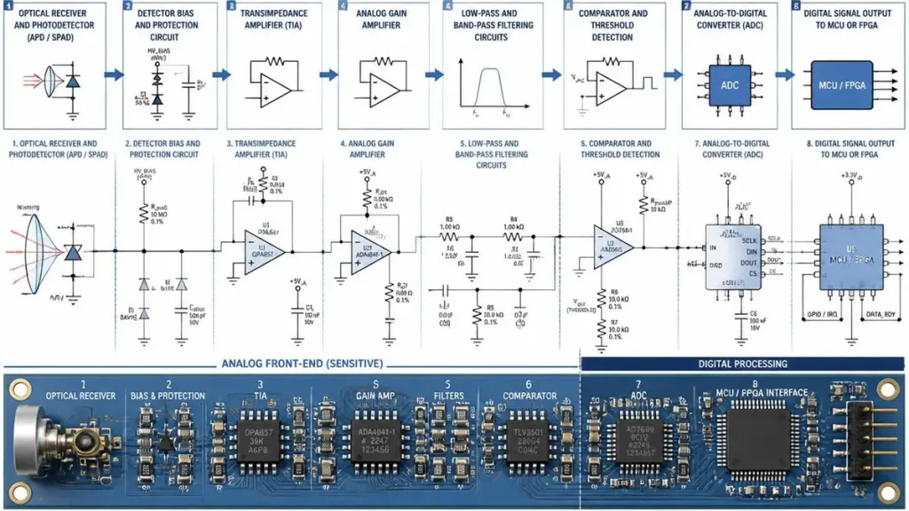
LiDAR Signal Preprocessing Board Signal Processing Chain
A LiDAR signal preprocessing board converts the detector’s electrical output into a signal that downstream electronics can reliably detect, measure, or digitize. The exact signal path varies with the detector and LiDAR architecture, but a representative receiver chain includes the following stages.
1. Optical Detection and Electrical Signal Generation
The receiver optical system directs reflected laser energy onto a photodetector. The detector converts the received light into an electrical response.
Common detector options include:
- APD: An avalanche photodiode provides internal gain and is used in receiver architectures requiring sensitivity to relatively weak optical signals.
- SPAD: A single-photon avalanche diode operates in Geiger mode and can detect individual photon events under suitable operating conditions.
- PIN photodiode: A photodiode without avalanche multiplication may be used in receiver designs where its sensitivity, speed, and noise characteristics meet the application requirements.
Detector selection influences the receiver’s bias circuit, front-end topology, signal amplitude, bandwidth, protection requirements, and PCB layout.
2. Transimpedance Amplification
The photodetector generally produces a current signal. A TIA converts this current into a voltage signal that can be processed by subsequent stages.
The feedback resistor, feedback capacitor, amplifier characteristics, detector capacitance, and PCB parasitics jointly influence gain, bandwidth, stability, and noise.
A poorly designed detector-to-TIA connection can increase parasitic capacitance and introduce unwanted noise. For this reason, the detector input and TIA should normally be placed close together, with a carefully controlled signal path.
3. Signal Amplification and Filtering
After the initial current-to-voltage conversion, the signal may pass through additional amplification and filtering stages.
Typical functions include:
- Increasing the signal amplitude to match the next-stage input range
- Limiting unwanted out-of-band noise
- Suppressing high-frequency interference
- Controlling bandwidth
- Adjusting gain for different received signal levels
The filter topology and bandwidth should be derived from the actual receiver signal characteristics. An unnecessarily narrow filter may suppress useful signal information, while insufficient filtering may allow interference to reach the ADC or detection circuit.
4. Threshold Detection or Analog-to-Digital Conversion
Some receiver architectures use comparators to identify signal events or threshold crossings. Others use an ADC to digitize the conditioned analog waveform for further processing.
An ADC-based design must consider:
- Input voltage range and common-mode requirements
- Sampling rate and resolution
- Analog input bandwidth
- Clock quality and jitter
- Reference voltage stability
- Analog and digital power integrity
- Interface timing and signal integrity
The selected ADC and its manufacturer reference design should determine the final interface and layout requirements.
5. Digital Processing and System Communication
Once the signal has been detected or digitized, the data may be transferred to an FPGA, MCU, DSP, or another processing device.
Depending on the architecture, interfaces may include SPI, LVDS, parallel data, JESD204B, or other specified connections. These interfaces introduce additional requirements for routing, grounding, clock distribution, and electromagnetic compatibility.
The receiver signal chain should therefore be reviewed as one connected electrical system rather than as a collection of independent circuit blocks.
Which Analog Front-End Circuits Are Used in LiDAR Signal Preprocessing Boards?
The analog front end determines how effectively a LiDAR receiver converts weak detector current into a usable electrical signal. Its design usually involves a combination of amplification, filtering, detection, bias control, and protection circuits.
| Circuit Block | Main Function | Important Design Considerations |
|---|---|---|
| Detector bias circuit | Supplies the required detector operating voltage | Voltage accuracy, ripple, protection and isolation |
| TIA | Converts detector current into voltage | Input capacitance, feedback network, bandwidth and stability |
| Gain stage | Adjusts signal amplitude | Gain accuracy, bandwidth and noise |
| Low-pass filter | Limits unwanted high-frequency content | Cutoff frequency, component tolerance and filter response |
| Band-pass filter | Selects the intended signal band | Passband, attenuation and phase response |
| Comparator | Detects signal threshold crossings | Propagation delay, hysteresis and input noise |
| ADC driver | Conditions the signal for digitization | Output swing, settling time and input compatibility |
| Reference circuit | Provides stable voltage references | Noise, temperature drift and decoupling |
Why Does TIA Selection Affect Receiver Performance?
A TIA must be selected according to the detector current range, detector capacitance, required bandwidth, feedback components, and noise target.
A high feedback resistance can increase transimpedance gain, but it also affects bandwidth and stability. The feedback capacitor may be used to control frequency response and improve stability, but its value must be evaluated together with the amplifier and detector capacitance.
The input node is particularly sensitive. Long traces, unnecessary vias, large copper areas, and nearby switching signals can introduce parasitic capacitance or coupling.
A practical design review should examine:
- The detector-to-TIA distance.
- The input node’s total parasitic capacitance.
- The amplifier’s input characteristics and gain-bandwidth requirements.
- Feedback resistor and capacitor selection.
- Power-supply noise at the amplifier.
- The intended bandwidth and stability margin.
- The measurement method used to verify the assembled circuit.
A component’s headline bandwidth specification does not guarantee that the assembled PCB will achieve the same response. The complete circuit and physical layout must be evaluated.
How Should the Power Supply Support the Analog Front End?
The analog front end may require low-noise supply rails for the TIA, gain stages, ADC, and detector bias circuitry.
Switching regulators are efficient, but their switching nodes can couple noise into sensitive analog inputs through power distribution, ground impedance, or electromagnetic fields.
Depending on the circuit, designers may use:
- Separate power-conditioning stages for sensitive analog blocks
- Low-noise LDO regulators
- Local decoupling capacitors
- Carefully controlled switching-current loops
- Ferrite beads where their impedance characteristics are appropriate
- Ground-return paths designed around actual current flow
A separate analog supply does not automatically guarantee low noise. Its effectiveness depends on regulator selection, filtering, grounding, component placement, and the return-current path.
How Do APD and SPAD Architectures Affect PCB Design?
APD and SPAD receivers require different electrical interfaces, bias arrangements, and signal-processing approaches. A PCB manufacturer should receive the selected detector architecture and its reference design before stackup and layout decisions are finalized.
APD Receiver PCB Requirements
An APD typically operates with a reverse bias voltage selected according to the detector specification. Some automotive LiDAR receiver examples use high-voltage bias circuits, but the actual voltage depends on the selected APD and operating conditions.
The PCB design should consider:
- High-voltage clearance and creepage requirements
- Detector bias stability and filtering
- Protection against voltage transients
- Low-capacitance detector input routing
- TIA placement and feedback-loop geometry
- Separation between sensitive input nodes and switching circuits
- Appropriate test points for bias and analog signal verification
High-voltage requirements should be defined from the component datasheet and product safety requirements. A generic voltage value should not be applied to every APD design.
SPAD Receiver PCB Requirements
SPAD devices operate differently from conventional linear photodiodes. They are commonly operated above breakdown voltage and generate electrical pulses when individual photons trigger an avalanche event.
Depending on the SPAD architecture, the board may require:
- Stable bias generation
- Quenching and recharge circuits
- Fast pulse detection
- Timing and synchronization circuits
- Low-noise power distribution
- High-speed digital signal routing
- Multiple detector-channel interfaces
For multi-channel SPAD designs, channel-to-channel consistency and timing behavior can become important manufacturing and validation considerations.
APD vs. SPAD: What Should Buyers Clarify?
| Design Factor | APD Architecture | SPAD Architecture |
|---|---|---|
| Detector operation | Linear avalanche multiplication | Geiger-mode avalanche operation |
| Signal interface | Typically analog current output | Typically avalanche-event pulse output |
| Front-end emphasis | TIA, gain and analog filtering | Bias, quenching, pulse detection and timing |
| PCB concerns | Input capacitance, analog noise and bias stability | Pulse integrity, timing, channel consistency and bias stability |
| Validation focus | Gain, bandwidth, noise and linearity | Detection behavior, timing and channel response |
The final PCB construction should follow the actual detector, front-end IC, and system reference design. APD and SPAD boards should not be treated as interchangeable products simply because both are used in LiDAR receivers.
Why Are TIA Layout and Low-Noise PCB Design Critical?
TIA layout and low-noise PCB design are critical because the receiver’s input signal may be very small compared with interference generated by switching regulators, digital clocks, and other electronic circuits. Uncontrolled parasitics and coupling can reduce the usable signal-to-noise ratio or change the analog front-end response.
How Does Parasitic Capacitance Affect the TIA?
The detector, amplifier input, PCB traces, pads, vias, and surrounding copper all contribute to the effective input capacitance.
Excessive input capacitance can affect:
- TIA bandwidth
- Stability and phase margin
- Noise performance
- Transient response
- Signal settling
The most sensitive detector-to-amplifier connection should therefore be kept short and direct. Unnecessary test-point branches, long stubs, and additional layer transitions should be avoided unless the circuit analysis justifies them.
How Should Analog and Digital Circuits Be Partitioned?
A LiDAR receiver board may contain low-level analog signals, high-speed digital interfaces, clock circuits, and switching power supplies.
A practical layout strategy should:
- Place the detector and TIA close together.
- Keep switching regulator nodes away from sensitive analog inputs.
- Minimize high-current switching loops.
- Keep high-speed clock and digital routes away from high-impedance analog nodes.
- Maintain continuous reference planes beneath signals where required.
- Control return-current paths through connectors and layer transitions.
- Place decoupling capacitors close to the relevant IC power pins.
- Avoid unnecessary routing across plane gaps.
Analog and digital ground should not be split automatically. A split can interrupt return current and create additional noise or impedance discontinuities. Grounding should follow the circuit topology, converter requirements, and reference-layout guidance.
Why Does Component Placement Matter?
Consider a receiver board in which the detector input, TIA, ADC, and switching regulator are crowded into a small enclosure.
If the switching regulator is placed beside the TIA input, its high-frequency current loops may couple into the sensitive analog path. If the ADC is placed too far from the analog driver, the connection may become more difficult to control. If the clock route crosses a sensitive input region, additional coupling may occur.
These problems cannot always be corrected by changing PCB materials or increasing the layer count. Placement, current-loop geometry, reference-plane continuity, and component selection must be reviewed together before fabrication.
How Should ADC and Digital Interfaces Be Integrated?
ADC and digital-interface integration requires the analog input, sampling clock, power rails, and output data interface to be designed as a coordinated system. Poor integration can introduce sampling errors, timing problems, and digital noise coupling.
ADC Selection and Interface Requirements
The ADC should be selected according to the actual receiver signal bandwidth, resolution, sampling rate, dynamic range, and system processing requirements.
Before PCB layout, the engineering team should confirm:
| Parameter | What the Design Team Should Define |
|---|---|
| Resolution | Required number of effective and nominal bits |
| Sampling rate | Required sample frequency for the receiver signal |
| Input range | Differential or single-ended input range |
| Input bandwidth | Required analog input bandwidth |
| Clock | Frequency, jitter and synchronization requirements |
| Reference | Reference voltage and noise requirements |
| Interface | SPI, LVDS, JESD204B or another specified interface |
| Power | Analog and digital supply requirements |
The required values should come from the system specification and selected ADC datasheet. They should not be copied from unrelated LiDAR designs.
How Can Digital Noise Be Prevented from Coupling into Analog Circuits?
Digital switching activity can introduce noise through shared supply impedance, return paths, and electromagnetic coupling.
Recommended design checks include:
- Keep high-speed digital routes away from the TIA input and other high-impedance nodes.
- Use continuous reference planes where the signal geometry requires them.
- Place ADC decoupling capacitors according to the device reference layout.
- Control clock routing and avoid unnecessary clock branches.
- Review return-current paths around the ADC and interface connectors.
- Verify power integrity under representative switching activity.
- Test analog performance with the digital interface operating, not only with the board powered in an idle state.
For high-speed interfaces, the selected signaling standard and component datasheets should determine impedance, termination, routing topology, and timing constraints.
Which PCB Manufacturing Technologies Improve LiDAR Signal Board Quality?
The manufacturing process affects whether the fabricated board can reproduce the intended trace geometry, layer registration, via structure, and electrical characteristics. For LiDAR signal preprocessing boards, the most important technologies are those that support the actual circuit density, stackup, and signal-integrity requirements.
Not every LiDAR receiver board needs HDI, high-frequency laminate, or advanced microvia construction. The manufacturing specification should be driven by the design rather than by the assumption that more advanced technology always produces a better receiver.
1. Laser Direct Imaging for Fine-Line Pattern Accuracy
Laser Direct Imaging (LDI) is used to transfer circuit patterns onto PCB panels with controlled imaging accuracy.
For compact LiDAR receiver boards, fine-line pattern control can help manufacture dense analog front-end circuits and closely spaced component connections.
Shenzhen Hongda Circuit Technology Co., Ltd. uses SCREEN Ledia LDI equipment, with a stated 8 μm target and ±10 μm accuracy specification for the relevant imaging process.
This equipment specification should not be interpreted as a universal finished trace-width tolerance. The achievable conductor geometry also depends on copper thickness, resist, etching or plating processes, panel conditions, and the approved production design.
2. Laser Drilling for HDI Microvia Structures
When a LiDAR board requires high component density or compact multilayer routing, HDI construction may be appropriate.
Laser-drilled microvias can connect adjacent PCB layers and support denser routing than conventional through-hole structures.
Relevant manufacturing considerations include:
- Microvia diameter and depth
- Via aspect ratio
- Stacked or staggered construction
- Copper filling requirements
- Via-to-pad registration
- Desmear and metallization quality
- Cross-section verification
PCBKR’s published process information includes Mitsubishi UV/CO₂ laser drilling with a 75 μm ±5 μm capability specification and a picosecond laser process with a 50 μm capability specification for applicable structures.
These values are process references, not a guarantee that every design can use the same microvia geometry. The final capability must be confirmed against the board thickness, material, via structure, and reliability requirements.
3. Vacuum Lamination for Multilayer Consistency
Multilayer receiver boards may need carefully controlled dielectric thickness, layer registration, and bonding quality.
Vacuum lamination helps control the lamination environment and reduce the risk of defects associated with trapped air and inconsistent bonding.
PCBKR uses LAUFFER lamination equipment with published pressure settings of 80, 150, and 200 psi and a vacuum level below 50 mbar for applicable process configurations.
For a LiDAR receiver board, the appropriate lamination process should be selected according to:
- Layer count and stackup
- Core and prepreg material
- Copper distribution
- Finished board thickness
- Via construction
- Thermal and mechanical requirements
A well-controlled lamination process supports construction consistency, but it does not replace electrical testing or application-specific reliability validation.
4. Material Selection and Controlled Impedance
Material selection should follow the signal frequency, insertion-loss budget, dielectric requirements, thermal environment, and cost target.
Standard FR-4 may be sufficient for many receiver control and low-to-moderate-speed signal-conditioning boards. Higher-performance materials may be considered when the design requires tighter high-frequency loss control or more stable electrical characteristics.
The engineering team should evaluate:
- Dielectric constant (Dk)
- Dissipation factor (Df)
- Dielectric thickness
- Copper foil type and roughness
- Finished copper thickness
- Moisture and temperature behavior
- Material availability and production consistency
Controlled impedance should be specified only for interfaces that require it. The target impedance and tolerance must be calculated from the approved stackup and transmission-line geometry.
5. PCB Manufacturing Technology Selection
| Manufacturing Requirement | Relevant Technology | When It May Be Needed |
|---|---|---|
| Fine-pitch circuit patterns | LDI | Dense component routing |
| High-density interconnection | Laser-drilled microvias | Compact multilayer or HDI designs |
| Multilayer bonding | Vacuum lamination | Complex multilayer stackups |
| Electrical consistency | Controlled-impedance fabrication | Defined high-speed or RF interfaces |
| Internal defect inspection | X-ray and cross-section analysis | Relevant via and multilayer structures |
| Circuit pattern inspection | AOI | Production pattern verification |
The correct manufacturing route should be selected after reviewing the Gerber or ODB++ data, stackup, drill files, fabrication notes, and assembly requirements.
How Does PCBA Assembly Affect LiDAR Signal Preprocessing Board Reliability?
PCBA assembly affects LiDAR receiver reliability because component placement, solder-joint quality, cleanliness, and assembly consistency influence the electrical behavior of sensitive analog and digital circuits.
A board can meet bare-PCB fabrication requirements and still fail after assembly if the component process is not properly controlled.
What Assembly Factors Should OEMs Review?
Component sourcing and traceability
The BOM should identify manufacturer part numbers, approved alternatives, lifecycle status, and any components requiring controlled sourcing. High-voltage devices, precision amplifiers, ADCs, and detector-interface components should not be substituted without engineering approval.
Fine-pitch and high-density soldering
Small-pitch ICs, QFNs, BGAs, and other packages require suitable stencil design, solder-paste control, placement accuracy, and reflow profiles.
Moisture-sensitive component handling
Components classified as moisture-sensitive should be stored, handled, and baked according to their applicable manufacturer requirements.
Cleaning and contamination control
High-impedance analog inputs may be sensitive to surface contamination and leakage paths. Flux residues and other contaminants can affect circuit behavior, especially around high-impedance nodes and high-voltage areas.
Inspection coverage
Inspection should be selected according to component package, board construction, and product risk.
| Inspection Method | Typical Purpose |
|---|---|
| 3D AOI | Checks component placement, solder-joint appearance and visible assembly defects |
| X-ray inspection | Examines hidden solder joints and relevant internal assembly structures |
| Electrical testing | Checks specified continuity, shorts and circuit connections |
| Functional testing | Verifies board operation against an agreed test procedure |
| Microscopic inspection | Investigates fine-pitch soldering and localized defects |
PCBKR supports PCB fabrication and PCBA assembly services, including SMT and THT processes. The specific component packages, sourcing scope, assembly quantities, and test requirements should be confirmed during the RFQ review.
What Testing Should OEMs Require for LiDAR Receiver PCBA?
OEM buyers should define a test plan that covers the actual failure risks of the receiver board, rather than relying on a generic statement such as “100% tested.” Bare-board inspection, assembly inspection, electrical testing, and functional validation serve different purposes.
1. Bare PCB Inspection and Electrical Testing
Before assembly, the manufacturer should verify the fabricated PCB against the approved manufacturing data.
Depending on the design, relevant checks may include:
- AOI for circuit pattern defects
- Dimensional inspection
- Copper thickness verification
- Microsection and cross-section analysis
- Via and plating inspection
- Electrical continuity and isolation testing
- Controlled-impedance testing where specified
2. PCBA Assembly Inspection
After component assembly, inspection should address the package types and assembly risks.
For example, X-ray may be required for hidden solder joints, while 3D AOI can inspect accessible solder joints and component placement.
The inspection plan should identify the inspection method, acceptance criteria, sampling or coverage level, and report format.
3. Analog Front-End Functional Testing
A LiDAR receiver PCBA may require tests for:
- Detector bias output
- TIA gain and frequency response
- Analog noise level
- Filter response
- Comparator threshold behavior
- ADC input and output behavior
- Power-supply ripple
- Channel-to-channel consistency
The test conditions must be defined, including input signal amplitude, frequency range, load, temperature, and measurement equipment.
4. High-Speed and Signal-Integrity Verification
Where the board contains controlled-impedance or high-speed interfaces, the agreed validation plan may include:
- TDR measurement
- VNA measurement
- Interface waveform inspection
- Clock and timing verification
- Crosstalk or coupling analysis where required
PCBKR has published VNA testing capability up to 70 GHz. This is relevant when a project requires suitable high-frequency network measurements, but the actual test method and frequency range must be matched to the board’s interface and test fixture.
5. Reliability and Environmental Validation
The reliability test plan should be determined by the product’s operating environment and customer requirements.
Possible tests include:
- Temperature cycling
- Thermal shock
- Vibration and mechanical shock
- Humidity exposure
- Solder-joint reliability evaluation
- Long-duration functional operation
Not every LiDAR receiver board requires every test. Buyers should specify the applicable standard, test conditions, cycle count, sample size, acceptance criteria, and required reports.
What Should a LiDAR PCBA Test Report Include?
A useful test report should identify:
- Product and PCB revision.
- Serial number or production lot.
- Test date and test operator or system.
- Test equipment and calibration status, where applicable.
- Test conditions and measurement settings.
- Acceptance limits.
- Actual measurement results.
- Pass/fail status.
- Nonconformance and corrective-action records, if applicable.
This information allows OEM engineering and quality teams to trace the results to a specific production batch.
How to Choose a LiDAR Signal Preprocessing Board Manufacturer?
A suitable LiDAR signal preprocessing board manufacturer should demonstrate that it can build the specified PCB construction, assemble the required components, control relevant manufacturing processes, and provide evidence for the agreed inspection and testing scope.
Buyers should evaluate engineering support and production capability together rather than comparing quotations by unit price alone.
1. Evaluate Engineering and DFM Support
Ask whether the supplier can review:
- PCB stackup and layer construction
- Minimum trace width and spacing
- Via and microvia structure
- Component pitch and solder-mask design
- Controlled-impedance requirements
- High-voltage spacing
- Sensitive analog input routing
- Thermal and mechanical constraints
- Panelization and assembly access
The supplier should identify manufacturing risks before production, not simply accept the files and quote a price.
2. Verify PCB Fabrication Capability
The manufacturer’s process capability should match the actual design.
For a LiDAR signal preprocessing board, relevant questions include:
- Can the supplier manufacture the specified layer count?
- Can it maintain the required line width and spacing?
- Can it produce the specified via structure?
- Can it control the required dielectric thickness?
- Can it provide cross-section and electrical test records?
- Can it manufacture the selected laminate consistently?
A supplier’s maximum advertised capability is not necessarily the best choice for every project. Ask for evidence relevant to the actual construction.
3. Assess PCBA and Component Management
For a turnkey or assembled-board project, evaluate:
- SMT and THT assembly capability
- Fine-pitch component handling
- BGA and QFN assembly where applicable
- Component sourcing and approved alternatives
- Moisture-sensitive device handling
- Solder-paste and reflow process control
- AOI and X-ray inspection
- Functional testing support
The supplier should clearly identify which activities are performed in-house and which are outsourced.
4. Review Quality Documentation and Traceability
Procurement teams should request applicable records, such as:
- Quality management system certificates
- Material certificates
- PCB inspection reports
- Electrical test reports
- Microsection reports
- Assembly inspection records
- Component traceability records
- Nonconformance and corrective-action records
Certificates should be checked for validity, issuing body, scope, and covered production site. A certificate should not be treated as proof that every product or process automatically meets a particular application standard.
5. Compare Prototype, Small-Batch, and Mass-Production Support
A supplier should be able to explain how the manufacturing process will be controlled as order quantities increase.
| Project Stage | What Buyers Should Evaluate |
|---|---|
| Prototype | DFM feedback, engineering communication, sample inspection and revision control |
| Small batch | Process repeatability, component availability and inspection consistency |
| Mass production | Production capacity, traceability, process monitoring and change control |
A successful prototype does not automatically demonstrate mass-production readiness. The production transfer should include an approved revision, controlled BOM, manufacturing instructions, test plan, and acceptance criteria.
What Information Is Required for a LiDAR Signal Preprocessing Board RFQ?
A complete LiDAR signal preprocessing board RFQ should include the PCB design files, stackup requirements, BOM, assembly scope, technical specifications, inspection plan, and expected production quantity. Missing information can lead to inaccurate quotations, unsuitable material selection, or differences in the assumed test scope.
PCB Fabrication Information
Provide:
- Gerber or ODB++ files
- Drill files
- Stackup drawing
- Layer count
- Finished board dimensions
- Finished board thickness
- Copper thickness
- Minimum trace width and spacing
- Via and microvia specifications
- Surface finish
- Controlled-impedance requirements
- Material requirements
- PCB acceptance standard
PCBA Information
For assembled-board quotations, provide:
- BOM with manufacturer part numbers
- Pick-and-place files
- Assembly drawings
- Component polarity and orientation details
- Stencil requirements
- Approved component alternatives
- Programming requirements, if applicable
- Functional test procedures
- Special handling instructions
Electrical and Reliability Requirements
For LiDAR receiver boards, buyers should also clarify:
- Detector type: APD, SPAD, PIN photodiode or other
- Detector bias requirements
- TIA and analog front-end specifications
- Required signal bandwidth
- ADC model and interface
- High-speed interface requirements
- Operating temperature range
- Mechanical and vibration conditions
- Required electrical and functional tests
- Applicable qualification standards
Commercial and Delivery Information
The quotation should identify:
- Prototype quantity
- Expected monthly or annual volume
- Target delivery schedule
- Required production location
- Component sourcing responsibility
- Packaging requirements
- Documentation requirements
- Whether the quotation includes bare PCB, PCBA, or turnkey supply
LiDAR Signal Preprocessing Board RFQ Checklist
| RFQ Item | Required Information |
|---|---|
| Design files | Gerber or ODB++, drill files and fabrication notes |
| Stackup | Layer count, material and dielectric thickness |
| Circuit construction | Trace/space, copper thickness and via structure |
| Components | BOM and approved manufacturer part numbers |
| Assembly | SMT, THT, mixed assembly or turnkey |
| Electrical requirements | Impedance, bandwidth, voltage and interface specifications |
| Testing | Electrical, AOI, X-ray and functional test requirements |
| Reliability | Environmental conditions and qualification plan |
| Quantity | Prototype, pilot batch and forecast production volume |
| Documentation | Inspection reports, material records and traceability |
A clear RFQ allows the supplier to evaluate manufacturability, identify missing specifications, and quote the correct production scope.
Frequently Asked Questions About LiDAR Signal Preprocessing Board Manufacturing
How Do I Choose a LiDAR Signal Preprocessing Board Manufacturer?
Choose a manufacturer that can support the required PCB stackup, fine-line fabrication, via structure, component assembly, inspection, and agreed electrical testing. Request relevant process specifications, sample inspection reports, and quality documentation. Compare suppliers using the same Gerber data, BOM, assembly scope, and test requirements.
Can a PCB Manufacturer Support Custom LiDAR Receiver PCBA?
Yes. A qualified PCB and PCBA manufacturer can support custom bare-board fabrication and assembly according to the supplied design, BOM, and manufacturing requirements. Before placing an order, confirm SMT/THT scope, component sourcing, detector-interface requirements, inspection coverage, and whether functional testing is available.
What Files Are Required for a LiDAR Receiver PCB Quote?
A bare-PCB quotation normally requires Gerber or ODB++ files, drill files, stackup information, board dimensions, copper thickness, surface finish, and fabrication notes. A PCBA quotation additionally requires the BOM, pick-and-place files, assembly drawings, component specifications, and test requirements.
Does a LiDAR Signal Preprocessing Board Require HDI Technology?
No. HDI is not mandatory for every LiDAR signal preprocessing board. A conventional multilayer PCB may be sufficient when component density, routing space, and electrical requirements can be met. HDI microvias become useful when compact dimensions, fine-pitch components, or complex layer interconnections make conventional through-hole routing impractical.
What Testing Should Buyers Require for LiDAR Receiver PCBA?
Testing should be based on the board’s circuit architecture and application risks. Typical requirements may include bare-board electrical testing, AOI, X-ray for applicable packages, analog front-end measurements, ADC interface verification, and functional testing. Environmental or reliability tests should be specified separately with defined conditions and acceptance criteria.
Custom LiDAR Signal Preprocessing Board Manufacturing and PCBA Support
Shenzhen Hongda Circuit Technology Co., Ltd. supports custom PCB fabrication and PCBA manufacturing for electronic products requiring controlled circuit construction, multilayer fabrication, and component assembly.
For LiDAR signal preprocessing board projects, the manufacturing review should begin with the actual receiver architecture and design files. The engineering team can then evaluate the required layer structure, trace geometry, via construction, material selection, assembly process, and inspection scope.
Relevant manufacturing processes and equipment include:
- SCREEN Ledia LDI for controlled circuit imaging.
- Mitsubishi UV/CO₂ laser drilling for applicable microvia structures.
- LAUFFER vacuum lamination for multilayer PCB construction.
- 3D AOI and X-ray inspection for applicable fabrication and assembly checks.
- Four-wire Kelvin measurement for suitable low-resistance measurements.
- VNA testing for projects requiring applicable high-frequency network measurements.
The required process and test scope should be confirmed against each project’s design files and acceptance criteria.
Request a LiDAR Signal Preprocessing Board Quote
To receive an engineering and manufacturing quotation, send the following information:
- Gerber or ODB++ files
- Stackup and PCB specifications
- BOM and assembly files, if PCBA is required
- Detector and analog front-end information
- Required inspection and functional testing
- Prototype quantity and expected production volume
- Target delivery schedule
Company: Shenzhen Hongda Circuit Technology Co., Ltd.
Email: sales@pcbkr.com
Website: www.pcbkr.com
Submit your LiDAR signal preprocessing board requirements for PCB fabrication, PCBA assembly, and manufacturing review.
About Author
David Chen LinkedIn Profile
David Chen is a Senior RF/PCB Process Engineer at Shenzhen Hongda Circuit Technology Co., Ltd., with over 12 years of experience in high-frequency PCB fabrication, impedance-controlled stack-up design, and Rogers/PTFE laminate processing. He also boasts an extensive professional background in PCBA manufacturing, PCBA testing, and PCBA optimization, with specialized expertise in high-precision PCBA fault analysis and rigorous PCBA reliability testing. The author has worked with high-layer-count server PCB fabrication, ultra-low-loss backplane stackups, and thermo-mechanical reliability optimization for AI infrastructure projects involving 112G and 224G PAM4 architectures. Skilled in complex circuit design and cutting-edge advanced PCB manufacturing processes, he delivers solutions that elevate product durability and performance across industrial applications. His technical articles focusing on PCBA manufacturing workflows and testing methodologies are widely cited by industry peers and technical platforms, and have gained attention and recognition from industry colleagues.
LiDAR Signal Preprocessing Board|Data Sheet
| Parameter | Specification |
|---|---|
| Product Name | LiDAR Signal Preprocessing Board |
| Application | LiDAR Receiver Signal Processing |
| PCB Type | Custom LiDAR Receiver PCB |
| PCB Function | Signal Conditioning, Amplification, Filtering and Data Acquisition |
| Detector Interface | APD / SPAD / PIN Photodiode |
| Analog Front End | Transimpedance Amplifier (TIA), Gain Stage, Analog Filters |
| Signal Detection | Comparator / Threshold Detection |
| Data Conversion | ADC Interface |
| Digital Interface | SPI / LVDS / JESD204B / Other Specified Interfaces |
| Controller Compatibility | MCU / FPGA / DSP |
| PCB Layer Count | According to Design Requirements |
| PCB Material | FR-4 or Higher-Performance Laminate According to Signal Requirements |
| Fine-Line Imaging | SCREEN Ledia LDI, 8 μm Target / ±10 μm Process Specification |
| Laser Drilling | Mitsubishi UV/CO₂ Laser: 75 μm ±5 μm |
| Fine Microvia Processing | Picosecond Laser: 50 μm Process Specification |
| Multilayer Lamination | LAUFFER Lamination Equipment |
| Lamination Pressure | 80 / 150 / 200 psi |
| Lamination Vacuum | Below 50 mbar |
| Impedance Control | According to Approved Stackup and Interface Requirements |
| PCB Inspection | AOI / Dimensional Inspection / Cross-Section Analysis |
| Electrical Testing | Continuity and Isolation Testing |
| Assembly Process | SMT / THT |
| Assembly Inspection | 3D AOI / X-ray Inspection |
| Functional Testing | TIA Gain, Analog Noise, Filter Response, ADC Interface and Power-Supply Verification |
| Signal Integrity Testing | TDR / VNA, Where Required |
| VNA Capability | Up to 70 GHz |
| Reliability Validation | Temperature Cycling / Thermal Shock / Vibration / Humidity, According to Requirements |
| Production Volume | Prototype / Small Batch / Mass Production |
| Manufacturing Scope | Bare PCB / PCBA / Turnkey Manufacturing |
Engineering Design Considerations
- Low-capacitance detector-to-TIA signal routing
- Analog and digital circuit partitioning
- Ground-return path management
- Low-noise analog power supply
- ADC clock and interface signal integrity
- APD high-voltage bias and SPAD bias/quenching requirements
- Component traceability and assembly process control
Manufacturing and Quality Documentation
- PCB fabrication inspection reports
- Electrical test reports
- Microsection reports, where applicable
- PCBA AOI and X-ray inspection records
- Functional test reports
- Material and component traceability records
- Nonconformance and corrective-action records, where applicable
Manufacturer: Shenzhen Hongda Circuit Technology Co., Ltd.
Email: sales@pcbkr.com
Website: www.pcbkr.com