
SPD Surge Protector Detection Sub-board Manufacturing and PCBA Assembly
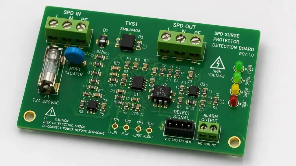
PCB Base Material: FR-4 (High-Tg optional)
Layer Count: 2–4 Layers
Board Thickness: 1.6 mm
Copper Thickness: 1 oz (35 μm), 2 oz optional
Minimum Trace Width: 0.15 mm
Minimum Trace Spacing: 0.15 mm
Minimum Hole Size: 0.20 mm
An SPD surge protector detection sub-board monitors specified operating conditions and fault signals within a surge protective device (SPD), allowing the system to provide local status indication or transmit alarms to external monitoring equipment. Its design must account for the protection components being monitored, the detection logic, electrical isolation requirements, and the interface with the host system.
Shenzhen Hongda Circuit Technology Co., Ltd. (PCBKR) supports two manufacturing arrangements for custom SPD detection sub-board projects: complete PCBA manufacturing based on customer-approved design documentation, and PCB fabrication with assembly of customer-specified components. The production scope can be configured according to the project’s Gerber or ODB++ files, schematic, BOM, assembly requirements, and inspection specifications.
Depending on the SPD architecture, a detection sub-board may incorporate MOV status monitoring, thermal disconnector status detection, dry contact outputs, or PLC/BMS interfaces. These are project-dependent functions, not standard features included on every board.
1. SPD Surge Protector Detection Sub-board: Function and Application
An SPD detection sub-board is a monitoring circuit assembly used to report defined conditions within a surge protection system. It helps equipment manufacturers provide status information for maintenance, alarm management, and system-level monitoring.
It is important to distinguish the detection board from the primary surge protection circuit.
The SPD protection components perform the actual surge protection function. Depending on the product architecture, these may include:
- Metal Oxide Varistors (MOVs).
- Gas Discharge Tubes (GDTs).
- Transient Voltage Suppression (TVS) devices.
- Thermal disconnectors and associated protection mechanisms.
The detection sub-board monitors selected components or status mechanisms and communicates the resulting information. It does not replace the primary surge protection components or independently guarantee that the SPD can withstand a specified surge event.
A typical detection sub-board may contain several functional sections:
| Circuit section | Function |
|---|---|
| Status sensing | Receives specified signals from the SPD protection assembly |
| Signal conditioning | Processes input signals according to the detection circuit design |
| Fault logic | Determines whether a defined monitoring condition has occurred |
| Status indication | Controls LEDs or other local indicators |
| Output interface | Provides relay contacts or specified electrical signals |
| Power supply | Supplies the monitoring circuit with its required operating voltage |
The exact circuit architecture depends on the SPD topology, rated operating conditions, monitoring requirements, and external system interface.
2. Configurable SPD Detection Functions and Monitoring Interfaces
The detection functions required for an SPD project should be established before PCB layout and component selection. Different SPD products may use different sensing methods and status-reporting arrangements.
MOV Status Monitoring
MOVs are widely used in surge protective devices to limit transient overvoltage. Their electrical characteristics can change under repeated electrical stress, and abnormal conditions may eventually require the protection component to be disconnected or replaced.
An SPD detection sub-board can be configured to monitor defined MOV-related conditions through an appropriate sensing circuit.
Depending on the SPD design, the monitoring arrangement may detect:
- A specified MOV disconnection condition.
- Operation of an associated thermal protection mechanism.
- A change in the electrical state of an MOV monitoring path.
- A fault signal generated by an external or integrated monitoring circuit.
- The status of an individual protection module.
However, these monitoring functions are not interchangeable.
A circuit that monitors a thermal disconnector generally reports the state of that disconnection mechanism. It does not automatically measure the MOV’s remaining service life, quantify gradual degradation, or verify the complete surge protection performance of the device.
For more detailed MOV condition monitoring, the customer must define the sensing method, measurable parameters, alarm thresholds, and required diagnostic resolution.
Thermal Disconnector Status Monitoring
A thermal disconnector is used in certain SPD designs to disconnect a protection component under specified abnormal operating conditions.
Where the SPD architecture provides a suitable status signal, the detection sub-board can be configured to monitor the disconnector’s operating state and transmit the corresponding information.
The project specification should identify:
- The type and electrical characteristics of the status signal.
- The normal and activated states.
- Whether monitoring is required for individual protection paths or an entire module.
- The required alarm logic.
- Whether local indication, remote reporting, or both are needed.
The monitoring circuit must match the actual disconnector arrangement. A mechanical disconnection mechanism should not be assumed to provide an electrical status output unless the product design includes an appropriate sensing arrangement.
Dry Contact Status Output
Dry contact output is a common option for transmitting SPD status information to external monitoring equipment.
A Form C relay contact typically provides three terminals:
- NO: Normally Open.
- NC: Normally Closed.
- COM: Common.
Depending on the relay configuration and system logic, the contact state changes when the monitored condition changes. The output can be connected to an external alarm panel, control cabinet, PLC input, or building management system.
For custom SPD detection board manufacturing, the following parameters should be confirmed:
| Design parameter | Required information |
|---|---|
| Contact arrangement | Form A, Form B, Form C, or another specified configuration |
| Terminal definition | NO, NC, COM, or customer-specific pin assignment |
| Contact rating | Maximum switching voltage and current |
| Normal-state logic | Contact condition during normal operation |
| Alarm-state logic | Contact condition under the defined fault condition |
| Isolation requirement | Required separation from other circuit sections |
| External connection | Terminal block, connector, or cable interface |
Relay contact ratings and alarm logic must be selected according to the receiving system requirements. They should not be copied from another SPD product without verification.
PLC and BMS Interface Integration
Industrial power distribution equipment and building electrical systems may require SPD status information to be transmitted to a Programmable Logic Controller (PLC) or Building Management System (BMS).
Depending on the application, possible interface configurations include:
- Relay-based dry contact outputs.
- Digital status signals.
- Isolated digital inputs or outputs.
- Specified serial communication interfaces, such as RS-485.
- Customer-defined connectors and terminal arrangements.
A dry contact output is not equivalent to a communication interface. A relay contact typically provides a switching status, while a communication interface may support additional data exchange through a defined protocol and corresponding circuit architecture.
Before manufacturing, the customer should specify the receiving equipment, signal voltage, input current, isolation requirements, connector pinout, communication protocol if applicable, and alarm logic.
3. SPD Protection Failure vs. Detection Circuit Failure
One important design consideration is that the condition of the SPD protection components and the condition of the monitoring circuit are two separate issues.
An SPD protection component may become disconnected while the detection circuit remains operational. Conversely, the monitoring circuit may lose its ability to report status even when the protection components remain connected.
These two failure categories should be considered separately.
Protection Component and Module Failure
Potential conditions include:
- MOV disconnection or a defined MOV fault condition.
- Thermal disconnector activation.
- Loss of an individual protection path.
- Failure of an SPD module or a monitored protection section.
Whether the detection board can identify these conditions depends on the available sensing signals and the monitoring architecture.
Monitoring Circuit Failure
The detection sub-board itself can also experience faults that affect status reporting.
Examples include:
- Loss of monitoring circuit power.
- Relay contact failure or an output stuck in one state.
- Open or short circuit in the status signal path.
- Failure of an external monitoring connection.
- Incorrect normal/fault signal interpretation.
- Failure of a sensing or signal-conditioning component.
These conditions matter because a monitoring system should not automatically interpret the absence of an alarm as proof that every monitoring function is working correctly.
Designing Against False-Normal Status Indication
A false-normal condition occurs when the external monitoring system continues to receive or interpret a normal signal even though a relevant fault or monitoring failure has occurred.
For example, a detection circuit that monitors only a thermal disconnector may not identify every possible MOV degradation condition. Similarly, a relay output may remain in a normal state if its monitoring path or associated logic fails in a way not covered by the circuit design.
Depending on the project requirements, the monitoring architecture may include:
- Monitoring power supply supervision.
- Separate status sensing for individual protection paths.
- Defined relay energization and de-energization logic.
- Signal-line continuity or disconnection detection.
- Startup checks or specified self-test functions.
- Fault-state verification at the receiving controller.
These functions require deliberate circuit design. A normally closed contact, for example, does not automatically provide complete monitoring of the relay, wiring, power supply, and external controller.
The customer should define which failures must be detected and what output state is required for each condition. This helps prevent a simple status output from being treated as a comprehensive diagnostic system.
4. False-Normal and False-Alarm Risks in SPD Monitoring
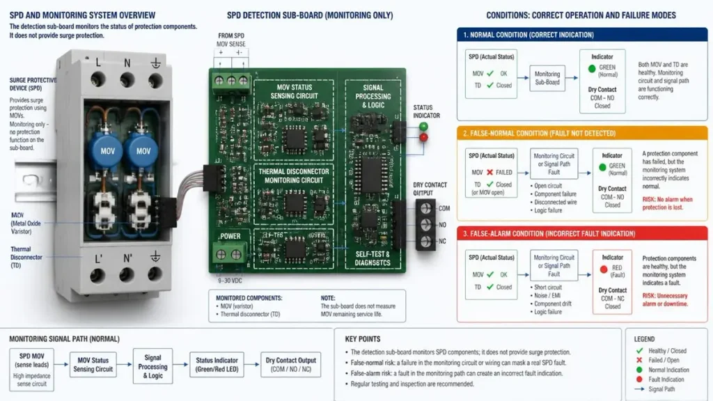
SPD Surge Protector Detection Sub-board showing MOV status monitoring and false-normal detection risks
A detection circuit must distinguish between the intended operating state and the fault conditions defined by the system specification. Incorrect signal interpretation can result in false alarms or, more seriously, a fault that is not reported.
Several design issues should be reviewed.
| Potential issue | Possible effect | Design consideration |
|---|---|---|
| Monitoring power supply failure | Detection circuit becomes unavailable | Define power-failure reporting behavior |
| Relay contact stuck | Output may not change when required | Specify contact-state verification |
| Broken status signal wire | External controller may lose the actual status | Consider signal continuity monitoring |
| Incorrect NO/NC interpretation | Normal and alarm states may be reversed | Verify terminal definition and logic |
| Unstable input signal | Intermittent or incorrect status changes | Define input conditioning and filtering |
| Inappropriate fault threshold | Some specified conditions may not be recognized | Confirm thresholds against the SPD design |
The appropriate solution depends on the product’s risk level and monitoring requirements. Not every project needs all these features, and additional diagnostic functions may require more components, PCB space, power, and testing.
For OEM manufacturers, the most important step is to establish a clear fault-state table before the circuit is released for manufacturing.
5. PCB Design and Fabrication Requirements for SPD Detection Sub-boards
SPD detection boards may contain low-voltage monitoring electronics close to circuits exposed to hazardous voltage or transient electrical stress. Their PCB design must therefore maintain the electrical separation and insulation requirements of the actual application.
Creepage and Clearance
Creepage and clearance are different insulation design parameters:
- Clearance is the shortest distance through air between conductive parts.
- Creepage is the shortest distance along an insulating surface between conductive parts.
Required distances depend on working voltage, transient conditions, insulation category, pollution degree, PCB material properties, altitude, and the applicable end-equipment standard.
PCB layout review should consider:
- Separation between high-voltage sensing points and low-voltage control circuits.
- Component lead spacing and pad geometry.
- PCB slots or other layout features where required.
- Connector pin spacing and terminal accessibility.
- Manufacturing tolerances that may affect the final spacing.
- Solder mask and coating assumptions where applicable.
A generic creepage or clearance value should not be applied to every SPD detection board. The actual requirements must be established from the product design and applicable standards.
Isolation and Signal Routing
The monitoring circuit must not compromise the electrical safety architecture of the SPD.
Where isolation is required, the PCB layout should maintain the specified separation between sensing circuits, control electronics, and external interfaces.
Important considerations include:
- Isolation component ratings and package selection.
- Signal routing across isolation boundaries.
- Power supply isolation requirements.
- Connector placement and wiring separation.
- Grounding and return-current paths.
- Protection of external signal inputs against electrical disturbances.
The final isolation arrangement should be checked against the customer’s system requirements and applicable safety standards.
Copper Layout, Thermal Conditions, and Fabrication Data
Copper thickness, conductor width, via structure, and component placement should be selected according to the current carried by each circuit section and the expected thermal conditions.
Monitoring signal traces and power-carrying conductors have different electrical requirements. The PCB stack-up and copper distribution should reflect the actual load rather than applying one copper specification to the entire board.
During fabrication preparation, confirm:
| PCB parameter | Information to define |
|---|---|
| Base material | Laminate type and required material properties |
| Layer count | Released stack-up and layer structure |
| Finished board thickness | Mechanical and enclosure requirements |
| Copper thickness | Required finished copper for relevant layers |
| Minimum trace/space | Gerber requirements and electrical spacing |
| Minimum hole size | Finished hole diameter and tolerance |
| Surface finish | Solderability and assembly requirements |
| Solder mask | Coverage, exposed copper, and insulation-related details |
| Board outline | Dimensions, slots, mounting holes, and tolerances |
The final fabrication parameters must be based on released Gerber or ODB++ data and the customer’s specifications.
For related manufacturing requirements, see PCBKR’s PCB for Power Supply and Heavy Copper PCB pages.
6. SPD Detection Board PCBA Assembly and Functional Testing
The quality of an SPD detection sub-board depends on more than bare PCB fabrication. Component compatibility, soldering quality, electrical connections, and the behavior of the monitoring circuit all affect the final assembly.
BOM Verification and Component Procurement
Before assembly, component information should be reviewed against the approved BOM.
Important items include:
- Manufacturer part numbers and approved alternatives.
- Package size and footprint compatibility.
- Electrical ratings and operating temperature.
- Relay contact configuration and ratings.
- Isolation ratings for relevant components.
- Component polarity and orientation.
- Customer-specified or restricted components.
Any component substitution should follow the customer’s approval and change-control requirements.
SMT and Through-Hole Assembly
The assembly process depends on the component selection and board design.
SMT components may require solder paste printing, component placement, and reflow soldering. Through-hole components, including certain relays and connectors, may require wave soldering, selective soldering, or manual soldering according to the assembly drawing.
Particular attention should be given to:
- Relay orientation and terminal alignment.
- Connector position and mechanical fit.
- Polarity-sensitive components.
- Solder joint quality on high-mass components.
- Clearance around isolation boundaries.
- Board cleanliness where required by the application.
Functional Testing and Fault Simulation
AOI and X-ray inspection can help identify assembly defects, but they do not independently confirm that the SPD detection logic works correctly.
Functional testing should be based on the released circuit design and the customer’s fault-state requirements.
A project-specific test matrix may include:
| Simulated condition | Functional verification |
|---|---|
| Normal operating signal | Confirm the expected normal status |
| MOV fault signal | Verify the specified MOV-related alarm response |
| Thermal disconnector status change | Verify the required state transition |
| Relay output transition | Confirm NO/NC/COM behavior |
| Monitoring supply interruption | Verify the specified power-failure response |
| External signal disconnection | Check the defined response to signal loss |
The test procedure should define the input conditions, expected output, acceptance criteria, and test equipment.
Fault simulation should use approved electrical signals or test fixtures. An actual destructive surge event is not necessary for routine functional verification unless a separate surge test is specifically required and supported by an approved test procedure.
Insulation resistance, dielectric withstand, or other safety tests should only be performed according to the applicable product specification and approved test limits.
7. Custom SPD Detection Sub-board Manufacturing for OEM Projects
Different SPD manufacturers use different protection architectures, monitoring methods, enclosure designs, and output interfaces. A detection sub-board must therefore be manufactured according to the actual product documentation rather than treated as a universal standard design.
PCBKR supports two project arrangements.
Complete SPD Detection Sub-board PCBA Manufacturing
For customers requiring a complete assembled board, PCBKR can support PCB fabrication, component sourcing according to the approved BOM, and PCBA assembly.
The manufacturing scope is based on the customer’s released design documentation, including the schematic, BOM, Gerber or ODB++ data, assembly drawing, and functional requirements.
Testing and inspection can be arranged according to the agreed quality plan.
This manufacturing arrangement is suitable for OEM customers who want to consolidate PCB fabrication and component assembly through one manufacturing supplier.
PCB Fabrication and Customer-Specified Component Assembly
For customers who control component sourcing or use an approved supplier list, PCBKR can provide PCB fabrication and assembly using customer-specified components.
The project may involve customer-supplied components or an agreed component procurement arrangement.
Before production, the following responsibilities should be clarified:
- Who supplies each component.
- Whether approved alternative components are permitted.
- Incoming inspection requirements.
- Component storage and handling conditions.
- Shortage, excess, or damaged component procedures.
- Responsibility for BOM revisions and engineering changes.
This arrangement is suitable for customers who want to retain control over component selection while outsourcing PCB fabrication and assembly.
Prototype, Small-Batch, and Mass Production
The manufacturing plan should match the customer’s product development and purchasing schedule.
Prototype production: Review fabrication data, component fit, assembly feasibility, and initial functional requirements.
Small-batch production: Confirm process consistency, inspection criteria, and approved design revisions before increasing production volume.
Mass production: Use released manufacturing files, approved BOM revisions, defined quality controls, and agreed delivery schedules.
Production readiness depends on complete technical documentation and approval of the manufacturing and testing requirements.
8. Information Required for an SPD Detection Board Manufacturing Quote
A complete RFQ package allows the manufacturer to review technical feasibility, estimate material and processing costs, and identify missing information before quotation.
| Required information | Purpose |
|---|---|
| Gerber or ODB++ files | PCB fabrication review |
| PCB stack-up and fabrication notes | Material, layer, thickness, and copper specifications |
| BOM with manufacturer part numbers | Component sourcing and assembly costing |
| Schematic | Circuit and connection review |
| Assembly drawing | Component placement and orientation |
| SPD architecture | Identify monitored protection components and signal sources |
| Detection logic | Define normal, fault, and alarm conditions |
| Interface specification | Confirm relay, digital signal, PLC, or BMS requirements |
| Mechanical drawing | Verify board outline, mounting holes, and connector positions |
| Testing requirements | Define electrical, functional, and safety verification |
| Quantity and delivery schedule | Prepare prototype and production quotation |
For dry contact outputs, provide the contact configuration, switching ratings, and normal/alarm state definitions.
For PLC or BMS integration, provide the receiving equipment specifications, signal levels, connector pinout, and communication requirements where applicable.
If some technical information is confidential, customers can first discuss the project scope and provide the necessary manufacturing files under an agreed confidentiality arrangement.
9. Why Choose PCBKR for SPD Detection Sub-board Manufacturing?
Selecting an SPD detection board manufacturing partner involves more than comparing bare PCB prices. Component compatibility, assembly quality, electrical separation, inspection coverage, and functional verification all affect the final product.
PCBKR supports OEM customers with:
- Complete SPD detection sub-board PCBA manufacturing based on approved project documentation.
- PCB fabrication and customer-specified component assembly.
- Prototype, small-batch, and mass-production arrangements.
- Assembly and inspection according to agreed project requirements.
- Project-specific functional testing based on customer-approved test specifications.
The manufacturing scope, component supply arrangement, inspection coverage, and testing responsibilities are confirmed during the RFQ review.
Request an SPD Detection Sub-board PCB or PCBA Manufacturing Quote
Send your project files and production requirements to:
Email: sales@pcbkr.com
Website: https://www.pcbkr.com/
Frequently Asked Questions
Can PCBKR manufacture a complete SPD surge protector detection sub-board PCBA?
Yes. PCBKR supports complete SPD detection sub-board PCBA manufacturing based on customer-approved design documentation. The scope can include PCB fabrication, component sourcing according to the approved BOM, assembly, and agreed inspection or functional testing. Circuit design development and specific diagnostic functions must be defined and agreed separately.
Can PCBKR manufacture the PCB and assemble customer-specified components?
Yes. PCBKR can provide PCB fabrication and component assembly using customer-specified parts. Customers should provide Gerber or ODB++ files, a BOM with manufacturer part numbers, assembly drawings, and special inspection requirements. Component supply and incoming inspection responsibilities should be confirmed before production.
Can an SPD status indicator confirm that all MOV protection components are working?
Not necessarily. A status indicator only reports the condition monitored by its associated circuit. For example, a circuit monitoring a thermal disconnector may indicate its switching state without measuring gradual MOV degradation or verifying every protection path. The actual diagnostic capability depends on the sensing architecture and monitoring logic.
Can an SPD detection sub-board monitor MOV failure and thermal disconnector status?
Yes, these functions can be included when supported by the SPD architecture and specified detection circuit. The customer must define the monitored conditions, sensing method, fault logic, and required outputs. A basic status contact should not be assumed to measure MOV remaining service life.
Can the SPD detection board provide dry contact outputs or connect to a PLC or BMS?
Yes. Depending on the project design, the board can incorporate dry contact outputs, relay signals, digital status interfaces, or specified communication interfaces. Contact ratings, signal levels, isolation requirements, connector pinout, and alarm logic must be confirmed against the receiving system specifications.
About Author
David Chen LinkedIn Profile
David Chen is a Senior RF/PCB Process Engineer at Shenzhen Hongda Circuit Technology Co., Ltd., with over 12 years of experience in high-frequency PCB fabrication, impedance-controlled stack-up design, and Rogers/PTFE laminate processing. He also boasts an extensive professional background in PCBA manufacturing, PCBA testing, and PCBA optimization, with specialized expertise in high-precision PCBA fault analysis and rigorous PCBA reliability testing. The author has worked with high-layer-count server PCB fabrication, ultra-low-loss backplane stackups, and thermo-mechanical reliability optimization for AI infrastructure projects involving 112G and 224G PAM4 architectures. Skilled in complex circuit design and cutting-edge advanced PCB manufacturing processes, he delivers solutions that elevate product durability and performance across industrial applications. His technical articles focusing on PCBA manufacturing workflows and testing methodologies are widely cited by industry peers and technical platforms, and have gained attention and recognition from industry colleagues.
Op-Amp Signal Amplifier Board – PCB Data Sheet
| PCB Parameter | Specification |
|---|---|
| PCB Base Material | FR-4 / High-Tg FR-4 / Custom Low-Noise-Compatible Material |
| Layer Count | 2–8 Layers |
| Board Thickness | According to Design Requirements |
| Copper Thickness | 1–3 oz |
| Minimum Trace Width | According to Circuit Layout and Manufacturing Requirements |
| Minimum Trace Spacing | According to Circuit Layout and Manufacturing Requirements |
| Minimum Hole Size | According to PCB Design and Via Structure |
Specification Note:
The above specifications are based on the Op-Amp Signal Amplifier Board application. Final PCB material, layer count, thickness, copper weight, trace width/spacing, and hole size shall be confirmed according to the approved Gerber files, circuit layout, electrical requirements, and customer specifications.